Mineralogical Characterization of Iron Ore Tailings from ...
Università degli Studi di Padova
Dipartimento di Scienze Chimiche
SCUOLA DI DOTTORATO DI RICERCA IN SCIENZA ED INGEGNERIA DEI MATERIALI
CICLO XXVIII
TESI DI DOTTORATO
Synthesis and characterization of transparent
conductive oxides for gas sensing, solar control
and transparent electrode applications
Direttore della Scuola : Ch.mo Prof. Gaetano Granozzi
Supervisore : Ch.mo Prof. Massimo Guglielmi
Dottorando : Marco Sturaro

2

3
Summary
Abstract .......................................................................................................... 6
Sommario ....................................................................................................... 8
1 Overview on transparent conducting oxides (TCOs) .................. 13
1.1 Introduction ........................................................................................... 13
1.2 TCOs electrical and optical properties ............................................... 17
1.3 Trend in development and main applications for transparent
conductive oxides ............................................................................................ 23
2 Colloidal synthesis of metal and metal oxide nanoparticles ....... 35
2.1 Introduction ........................................................................................... 35
2.2 Nanocrystals synthesis methodology and nanocrystals formation
mechanism....................................................................................................... 37
2.3 Heat-up synthesis .................................................................................. 45
3 Synthesis of TCOs nanoparticles .................................................. 53
3.1 Introduction ........................................................................................... 53
3.2 Hot injection synthesis of doped Zinc oxide nanoparticles .............. 54
3.3 Heat up synthesis of doped Zinc oxide nanoparticles ....................... 56
3.4 GZO Synthesis and nanocrystals characterization ........................... 58
3.4.1 Gallium doped zinc oxide synthesis ................................................. 58
3.4.2 XRD characterization ....................................................................... 60
3.4.3 Electron Microscopy characterization .............................................. 62
3.4.4 Optical characterization .................................................................... 65
3.5 AZO Synthesis and nanocrystals characterization ........................... 66
3.5.1 Aluminum doped zinc oxide synthesis ............................................ 66
3.5.2 XRD characterization ....................................................................... 67
3.5.3 Optical characterization .................................................................... 69

4
3.6 SZO Synthesis and nanocrystals characterization ............................ 69
3.6.1 Silicon doped Zinc oxide synthesis .................................................. 69
3.6.2 XRD characterization ....................................................................... 72
3.6.3 Electron microscopy characterization .............................................. 73
3.6.4 Optical characterization .................................................................... 76
3.7 GeZO Synthesis and nanocrystals characterization ......................... 77
3.7.1 Germanium doped zinc oxide synthesis ........................................... 77
3.7.2 XRD characterization ....................................................................... 78
3.7.3 Electron microscopy characterization .............................................. 79
3.7.4 Optical characterization .................................................................... 80
3.8 NTO Synthesis and nanocrystals characterization ........................... 81
3.8.1 Niobium doped titanium dioxide synthesis ...................................... 81
3.8.2 XRD characterization ....................................................................... 82
3.8.3 Electron microscopy characterization .............................................. 84
3.8.4 Optical characterization .................................................................... 85
3.9 Conclusions ............................................................................................ 85
4 TCOs thin films characterization and applications ................... 88
4.1 Introduction ........................................................................................... 88
4.2 Thin films standard deposition and treatments procedure .............. 89
4.3 Thin films characterizations ................................................................ 91
4.3.1 GZO thin films characterizations ..................................................... 91
4.3.1.1 XRD characterization .................................................................... 92
4.3.1.2 Electron microscopy characterization .......................................... 93
4.3.1.3 Optical characterization ............................................................... 94
4.3.2 AZO thin films characterizations ..................................................... 95
4.3.2.1 XRD characterization .................................................................... 95
4.3.2.2 Electron microscopy characterization .......................................... 96
4.3.2.3 Optical characterization ............................................................... 96
4.3.3 SZO thin films characterizations ...................................................... 97
4.3.3.1 XRD characterization .................................................................... 97
5
4.3.3.2 Electron microscopy characterization .......................................... 98
4.3.3.3 Optical characterization ............................................................... 99
4.3.4 GeZO thin films characterizations ................................................. 100
4.3.4.1 XRD characterization .................................................................. 100
4.3.4.2 Electron microscopy and XPS characterizations ....................... 101
4.3.4.3 Optical characterization ............................................................. 102
4.3.5 NTO thin films characterizations ................................................... 103
4.3.5.1 Electron microscopy and XPS characterizations ....................... 103
4.3.5.2 Optical characterization ............................................................. 105
4.4 TCOs thin films as transparent electrodes ....................................... 106
4.4.1 Introduction .................................................................................... 106
4.4.2 Treatments on thin films................................................................. 107
4.4.3 Electro-optical charterization ......................................................... 111
4.5 TCOs thin films as solar control coatings ........................................ 113
4.6 Conclusions .......................................................................................... 118
5 Gas Sensing properties of TCO films .......................................... 120
5.1 Gas Sensors overview ......................................................................... 120
5.2 TCOs thin films for gas sensing applications ................................... 122
5.3 TCO thin films Gas Sensing measurements ..................................... 126
5.4 Effect of platinum NPs on the gas sensing properties of TCOs films .
5.4.1 Platinum nanoparticles synthesis ................................................... 138
5.4.2 Gas sensing measurements ............................................................. 140
5.5 Conclusions .......................................................................................... 143
6 Conclusion and future prospect ................................................. 146
Appendix: Materials and Methods ................................................... 148
A.1 Chemicals and synthesis setup ............................................................. 148
A.2 Instrumentation ..................................................................................... 148
A.2.1. X-Ray Diffraction ....................................................................... 148

6
A.2.2. Electron Microscopy ................................................................... 149
A.2.3. Spectroscopic ellipsometry ......................................................... 149
A.2.4. X-Ray photoelectron spectroscopy ............................................. 150
A.2.5. Gas sensing tests.......................................................................... 150
A.3 Materials Recipes .................................................................................. 150
A.3.1. Substrates cleaning ...................................................................... 150
A.3.2. Optimized recipe for the synthesis of 10 nm Pt NPs .................. 150
7
Abstract
My thesis is focused on the synthesis of thin films of transparent conductive oxides (TCOs) by
colloidal approach for gas sensing applications, solar control and transparent electrode.
The work is mainly divided in three different parts.
In the first place on the development of nanoparticles of doped conductive oxides and
transparent by colloidal synthesis. In particular nanoparticles were synthesized using heat up
synthesis that do not require high temperature injection: doped ZnO with trivalent metals such
as aluminum and gallium, or doped with tetravalent elements such as Silicon and Germanium,
and Niobium doped TiO2 nanoparticles. Free electrons introduced into the crystal by dopants
lead to the development of peculiar optoelectronic properties, in particular the formation of a
LSPR in the near infrared. In the first part such nanoparticles are also characterized by different
techniques and are faced in particular the variations in their morphology and the optical
properties as a result of different concentrations of doping.
The second part examination was focused on the deposition of TCOs colloidal suspensions and
the characterization of TCOs thin film. One of the primary objectives was to obtain functional
thin films (such as transparent electrodes or coatings for solar control) using mild heat
treatments and through different approaches, using UV lamps or organic acids attacks in order
to eliminate most of the organic residues. In this way, by combining heat-up synthesis easily
scalable, depositions via spray coating or spin coating (which does not therefore require the use
of vacuum or expensive equipment) and heat treatments that do not require excessive
temperatures, it is possible to pave the way to an industrialization of the process.
The last part focuses on the use of such films for sensor applications, in particular for the
detection of H2 and NO2. LSPR is sensitive to changes of the dielectric constant in the
neighborhood of the particles, and to variation of charge density, allowing to monitor the gases
that interact with the oxide resulting in a shift in the wavelength of the LSPR peak. Optical gas
sensing and electrical gas sensing measurements were performed to evaluate different behavior
of different dopant concentrations. Measurements in the presence of blue LEDs were also
carried out, investigating the role of this radiation in the desorption kinetics of adsorbed
molecules. Finally Platinum nanoparticles influence on the detection of hydrogen was also
evaluated in order to improve the sensitivity of the sensor exploiting Pt catalytic activity.
8
Sommario
Il mio lavoro di tesi si è focalizzato sulla sintesi di film sottili di ossidi trasparenti e conduttivi
(TCOs) per via colloidale per applicazioni di gas sensing, solar control ed elettrodo trasparente.
Il lavoro è suddiviso principalmente in tre diverse parti.
La prima parte si concentra sullo sviluppo di nanoparticelle di ossidi dopati conduttivi e
trasparenti per via colloidale. In particolare sono stati sintetizzate, utilizzando sintesi heat-up
che non richiedono iniezione ad alta temperatura, nanoparticelle di ZnO dopato con metalli
trivalenti come Alluminio e Gallio, oppure dopato con elementi tetravalenti come Silicio e
Germanio, e nanoparticelle di TiO2 dopata con Niobio. Gli elettroni liberi introdotti nel cristallo
in seguito al drogaggio portano allo sviluppo di peculiari proprietà optoelettroniche, in
particolare alla formazione di una LSPR nel vicino infrarosso. Tali nanoparticelle sono state
caratterizzate mediante diverse tecniche che permettono di investigare in particolare le
variazioni della loro morfologia e delle proprietà ottiche a seguito di diverse concentrazioni di
dopante.
Nella seconda parte vengono invece approfonditi gli aspetti legati alla deposizione delle
sospensioni colloidali ottenute e alla caratterizzazione dei film sottili prodotti. Uno degli
obiettivi primari è ottenere film sottili funzionali (ad esempio come elettrodi trasparenti o per
rivestimenti solar control) utilizzando blandi trattamenti termici e attraverso diversi approcci,
tra cui irraggiamento UV o attacchi con acidi organici in modo da eliminare gran parte dei
residui organici. In questo modo, combinando sintesi heat up “non injection” facilmente
scalabili, deposizioni tramite spray coating o spin coating (che non richiedano quindi l’uso di
vuoto o apparecchiature costose) e trattamenti termici che non richiedano temperature
eccessive, è possibile aprire la strada ad una industrializzazione del processo.
L’ultima parte si focalizza sull’utilizzo di tali film per applicazioni sensoristiche, in particolare
per la rilevazione di H2 e NO2. La LSPR è sensibile ai cambiamenti della costante dielettrica
nell’intorno delle particelle ed alla variazione di densità di carica: ciò permette di monitorare i
gas che interagiscono con l’ossido analizzando lo spostamento in lunghezza d’onda del picco
plasmonico. Sono stati effettuate misurazioni di gas sensing ottico ed elettrico per valutare le
diverse performance dei TCOs a diversa concentrazione di dopante. Misurazioni in presenza di
LED blu sono state inoltre eseguite, investigando il ruolo di tale radiazione nella cinetica di
desorbimento delle molecole adsorbite. Infine è stata anche valutata l’influenza di

9
nanoparticelle di Platino sulla rilevazione di idrogeno al fine di migliorare la sensibilità del
sensore sfruttando l’attività catalitica di tali nanoparticelle.
This doctoral project has generated some results that have been published or presented at
international conferences. Presentations and publications (also papers in preparation) are listed
in the following.
Refereed Journal Publications
M Cittadini, M Sturaro, M Guglielmi, A Resmini, I G Tredici, U Anselmi-Tamburini, P Koshy,
C C Sorrell, A Martucci, “ZnO nanorods grown on ZnO sol–gel seed films: Characteristics and
optical gas-sensing properties”, Sensors and Actuators B: Chemical, 213:493-500 5 July 2015
B. Fabbri, A. Gaiardo, A. Giberti, V. Guidi, C. Malagù, A. Martucci, M. Sturaro, G. Zonta, S.
Gherardi, P. Bernardoni, “Chemoresistive properties of photo-activated thin and thick ZnO
films”, Sensors and Actuators B: Chemical, 23 June 2015
Luca Giancaterini, Carlo Cantalini, Michela Cittadini, Marco Sturaro, Massimo Guglielmi,
Alessandro Martucci, Alessandro Resmini, Umberto Anselmi-Tamburini, “Au and Pt
Nanoparticles Effects on the Optical and Electrical Gas Sensing Properties of Sol–Gel-Based
ZnO Thin-Film Sensors”, IEEE Sensors Journal, 2 February 2015
M.Sturaro, E. Della Gaspera, A.Martucci, M. Guglielmi, “Low temperature near infrared
plasmonic gas sensing of gallium doped zinc oxide thin films from colloidal inks”
in preparation
Wenliang Zhu, Shoichiro Kitamura, Marco Boffelli, Elia Marin, Marco Sturaro, Alessandro
Martucci, Giuseppe Pezzotti, “Defect luminescence in Ga-doped ZnO nanoparticles
synthesized by hot injection or non-injection methods”, in submission
B. Fabbri, A. Gaiardo, A. Giberti, V. Guidi, C. Malagù, A. Martucci, M. Sturaro, “Electrical,
Optical and Sensing Properties of Photo-activated ZnO Thin Films”,Procedia Engineering
12/2014; 87:148-151.

10
Presentations during national and international
conferences
SPIE OPTICS + PHOTONICS meeting 2015 San Diego, California, USA, 9th – 13th August
2015, “Low temperature near infrared plasmonic gas sensing of gallium doped zinc oxide thin
films from colloidal inks” (oral presentation)
PLASMONICA 2015 meeting Padova, Italia, 1st – 3rd July 2015 Palazzo Moroni, Padova, “Low
temperature near infrared plasmonic gas sensing of gallium doped zinc oxide thin films from
colloidal inks” (poster presentation)
Visits Overseas
1st April 2014 – 1st August 2014: Visiting researcher at CSIRO (Commonwealth Scientific and
Industrial Research Organization), Department of Material Science and Engineering,
Melbourne (VIC) Australia. Host: Dott. Jacek Jasieniak
Collaborations
The present work of thesis was realized thanks to a lot of fruitful collaborations:
Prof. Carlo Cantalini (University of L’Aquila) is acknowledged for the collaborations in the
electrical gas sensing field.
Prof. Gaetano Granozzi and Prof. Stefano Agnoli are acknowledged for XPS analyses.
Prof. Giovanni Mattei and Dt. Niccolò Michieli are acknowledged for SEM analysis.
Dt. Marco Bersani (University College of London) is acknowledged for TEM measurements.

11

12
13
Chapter 1
Overview on transparent conducting oxides
(TCOs)
1.1 Introduction
Transparent conductor materials, including transparent conducting oxides (TCOs), play a critical role
in many current and emerging optoelectronic applications due to their unique combination of
electronic conductivity and transparency in the visible region of the spectrum. TCOs can collect and
deliver electricity permitting light transmission in and out of a device, making these metal oxide thin
films ideal for several applications, like photovoltaics and displays. Given the current rapid growth
of the display and photovoltaic industries, there will be an increasing demand for new TCO materials
and low-cost methods of depositing them, for example via solution approach, used in this work.
This chapter will first focus on a brief history of TCO materials, then on the main optical and electrical
properties of these materials. Finally it is also necessary to discuss about recent trends on TCOs
development and main TCOs applications.
First of all, it’s necessary to remark that the combination of conductivity and transparency is usually
impossible in intrinsic stoichiometric oxides; however, it is achieved by producing them with a non-
stoichiometric composition or by introducing appropriate dopants.
As the usefulness of TCO thin films depends on both their optical and electrical properties, both
parameters should be considered together with environmental stability, abrasion resistance, electron
work function, and compatibility with substrate and other components of a given device, as
appropriate for the application. The availability of the raw materials and the economics of the
deposition method are also significant factors in choosing the most appropriate TCO material. The
selection decision is generally made by maximizing the functioning of the TCO thin film by
considering all relevant parameters, and minimizing the expenses.

14
TCO material selection only based on maximizing the conductivity and the transparency can be
faulty.
TCOs history began when Bädeker observed in 1907 that an evaporated film of cadmium oxidized
after exposure to air, was becoming transparent while maintaining its conductive properties [1]. For
CdO, which has a yellowish appearance, Bädeker obtained resistivities as low as 1.2 × 10⁻³ Ω*cm,
only one order of magnitude higher than the resistivity of indium tin oxide (ITO) films, the best TCO
material available so far. Following the birth of the electronics industry after the Second World War,
transparent electrodes were investigated for optoelectronic applications such as front electrodes in
photocells, heated windscreens/windows and antistatic windows [2]. Other TCOs were also
investigated, like SnO2, and proposed as a transparent heating layer for aeroplane cockpit windows
[3]. After the Second World War, scientists also investigated ZnO for use as a typical compound
semiconductor (such as GaAs or InP) in device applications. However, ZnO was first applied as a
thin layer for surface acoustic wave devices owing to its good piezoelectric properties, which were
discovered in the 1960s [4].
The broad industrial application of TCO materials began at the end of the 1960s, when scientists used
infrared light filters composed of tin or In2O3 on low-pressure sodium discharge lamps to increase
the lamp efficiency by reducing heat losses [5, 6]. With the advent of flat-panel display technology
around 1970, tin-doped indium oxide became the most commonly used TCO material for transparent
electrodes [7].
After the oil crisis at the beginning of the 1970s, the effective use of energy became an emerging field
of research and technology. Heat mirrors on window glass [8], low-emissivity (ε) coatings that control
the heat and light flux passing through a window, offered one possible route for saving energy. For
solar control applications the TCO coatings, which consist of doped oxide films (SnO2:F, Cd2SnO4
or ITO), are used only for their optical properties; in particular, their high reflectivity in the infrared
spectral range above a wavelength of about 1 μm. Now ITO is no longer used as a low-emissivity
coating owing to the high cost of indium, and cadmium stannate (Cd2SnO4) was abandoned because
of the toxicity of cadmium. Today, typical low-emissivity coatings consist of a three-layer stack on a
glass sheet, such as SnO2 (ZnO or Bi2O3), Ag, and SnO2 (ZnO or Bi2O3) [9, 10]. Such a stack can
achieve sheet resistances of Rs = 2.5-3.5 Ω/□ for an Ag thickness of about 12 nm [11]. The
manufacturing of low-emissivity glass coatings is a mature industrial process that generates 4,000
km2 of glass per year worldwide [12].
Another emerging application is the use of ‘conductive glasses’, TCO-coated glass for electrochromic
and thermochromic devices, which can be used to shadow buildings against direct solar radiation to
reduce the heat load [13]. Of the different possible TCO materials available, SnO2:X, ITO and ZnO:X

15
(where ‘X’ is a dopant) have gained widespread attention, owing to their bandgap energy of >3 eV,
which allows for applications in the visible and near-ultraviolet spectral range (down to 300 nm), and
their tipically low resistivities of around 10-3 Ω*cm or lower. Nowadays, ITO is the TCO material
with the lowest resistivity on a commercial scale, of the order of 1-2×10⁻⁴ Ω cm. ITO is used almost
exclusively as the transparent electrode in flat-panel displays [14, 15]. Tin oxide doped with fluorine
or antimony was instead the first TCO material used on an industrial scale, specifically for low-
emissivity coatings on glass [16]. Today, it is also used as a transparent electrode, especially in thin-
film solar cells based on the absorber materials a-Si:H or CdTe. The resistivity of tin oxide can be as
low as 5×10⁻⁴ Ω*cm. It is also used as a window and contact layer in thin-film solar cells, based on
the absorber materials a-Si:H and Cu(In,Ga)Se(S)2 [17].
The past three decades have seen incremental improvements with respect to basic TCO properties,
and the field of n-type TCOs has nearly reached maturity. Another new material is doped TiO2 (the
low-temperature polymorph anatase), which was introduced as a thin-film material by the Hasegawa
group in 2005. The researchers achieved resistivities of the order of 5×10⁻⁴ Ω cm for niobium or
tantalum doped TiO2. A big advantage of doped TiO2 is its excellent chemical stability, which can
be exploited for use in transparent and conductive protection layers.
A clear trend is apparent upon inspection of Table 1.1, which provides a select history of TC/TCO
materials and their processing. Many of the traditional TCO materials actually got their start using
chemical solution processes such as spray pyrolysis.
Table 1.1 History of transparent conductor materials and processing. Adapted from [18].
With the advent of vacuum-based physical vapor deposition (PVD) technologies, methods such as
sputtering and pulsed laser deposition (PLD) became the primary tools for research and industry.
PVD methods remain ideal for exploring new material systems because of their ability to yield dense
films with benchmark properties. However, there is now a drive for industrial applications to bring

16
TCO processing back to its roots, to chemical solution deposition. Atmospheric pressure solution
routes are an attractive alternative to conventional high-vacuum techniques due to their ease of
fabrication, scalability, and potential to lower device manufacturing costs. However, this potential
can have also drawbacks. While costs associated with equipment and operation for solution
deposition are projected to be lower than vacuum deposition methods, the costs associated with
chemical precursors (depending on their synthetic complexity), solvents, additives, and post-
processing criteria may be prohibitive [19, 20, 21].
Research and insight into the chemistries of these systems is important to overcome these potential
drawbacks, and this work try to get over of some of them.
The coexistence of electrical conductivity and optical transparency in these materials depends on the
nature, number, and atomic arrangements of metal cations in crystalline or amorphous oxide
structures, on the resident morphology, and on the presence of intrinsic or intentionally introduced
defects. This topic will be presented and briefly discussed in the next paragraph.
The important TCO semiconductors are impurity-doped ZnO, In2O3, SnO2, TiO2 and CdO, as well as
the ternary compounds Zn2SnO4, ZnSnO3, Zn2In2O5, Zn3In2O6, In2SnO4, CdSnO3, and multi-
component oxides consisting of combinations of ZnO, In2O3 and SnO2. Relation between elements
forming TCOs and their availability in nature is shown in figure 1.1.
Most of the TCO materials are n-type semiconductors, but p-type TCO materials are also researched
and developed. Such TCO include: ZnO:Mg, ZnO:N, IZO?, NiO, NiO:Li, CuAlO2, Cu2SrO2, and
CuGaO2 thin films. At present, these materials have not yet found place in current applications.
Figure 1.1 Mass fraction abundance of the elements in the Earth’s crust as a function of atomic number. Common TCO cations are
highlighted by colored circles and additional dopants by squares. Adapted from [22]

17
1.2 TCOs electrical and optical properties
TCOs are wide band gap semiconducting oxides, with conductivity σ in the range ~ 102-106 S/m. As
electrical conductivity is an important property of TCOs, a general understanding of electronic
properties is required. The conductivity is due to doping either by oxygen vacancies or by extrinsic
dopants. In the absence of doping, these oxides become very good insulators. Most of the TCOs are
n-type semiconductors. The electrical conductivity of n-type TCO thin films depends on the electron
density in the conduction band and on their mobility. Electrical conductivity (σ) is defined in units of
S cm-1 as:
σ = Neµ (1)
where N is the carrier concentration (cm-3), e is the carrier charge (C), and m is the mobility (cm2 (V
s)-1). The fundamental charge of an electron is 1.602*10-19 C. It is evident from equation 1 that the
conductivity is a function of two parameters: mobility and carrier concentration. Typical carrier
concentrations for a-InZnO are 1019-1021 cm-3 compared to 1022–1023 cm-3 for metals. Electron
mobility in a-InZnO ranges 10–50 cm2 (V s)-1 [23], which is similar to that of Cu (59 cm2 (V s)-1)
[24]. Mobility can be described as the ease in which carriers can move through the material. It is
defined in terms of the average scattering time (t) and the carrier effective mass (m*) as:
𝜇 =𝑒𝜏
𝑚∗ (2)
Equation 2 shows that in order to increase the mobility, the scattering time must be increased or the
effective mass must be decreased. The latter involves new material development. The former relates
to issues of film quality. In general, anything that inhibits the movement of carriers through a material
(decreases 𝜏) will result in a decrease in mobility and in a decrease in conductivity. According to
Matthiesens rule [24], resistivity arises from independent scattering processes which are additive,
such as scattering due to impurities, defects, and grain boundaries:
1
𝜇𝑡𝑜𝑡𝑎𝑙=
1
𝜇𝑖𝑚𝑝𝑢𝑟𝑖𝑡𝑦+
1
𝜇𝑑𝑒𝑓𝑒𝑐𝑡+
1
𝜇𝑔𝑏+⋯ (3)
The most important sources of scattering in typical semiconductor materials are ionized impurity
scattering and acoustic phonon scattering (also called lattice scattering). Grain boundary scattering is
only significant when grains are smaller than the mean free path of the electron. Phase separation and

18
porosity will result in further scattering. The latter is a particular concern in solution processing, as
pores can form when solvent and gaseous decomposition products leave the material. For crystalline
TCOs, strict control over the crystalline properties is required. Large grain growth often requires
high-temperature processing. However, high temperatures are not compatible with most flexible
substrates such as polymers.
Due to the large energy gap (Eg > 3 eV) separating the valence band from the conducting band, the
conduction band cannot be thermally populated at room temperature (kT~0.03 eV, where k is
Boltzmann’s constant), hence, stoichiometric crystalline TCOs are good insulators. To explain the
TCO characteristics, various population mechanisms and several models describing the electron
mobility were proposed. Some characteristics of the mobility and the processes by which the
conduction band is populated with electrons were shown to be interconnected by electronic structure
studies, e.g., that the mobility is proportional to the magnitude of the band gap. In the case of intrinsic
materials, the density of conducting electrons has often been attributed to the presence of
unintentionally introduced donor centers, usually identified as metallic interstitials or oxygen
vacancies that produced shallow donor or impurity states located close to the conduction band. The
excess or donor electrons are thermally ionized at room temperature, and move into the host
conduction band. However, experiments have been inconclusive to establish which of the possible
dopants was the predominant donor. Extrinsic dopants have an important role in populating the
conduction band, and some of them have been unintentionally introduced.
In a pure, defect-free material at 0 K, all lattice sites are occupied and all electrons occupy their
ground-state energy levels. However, free carriers can be produced intrinsically at temperatures above
0 K by the thermal (entropically driven) introduction of defects such as interstitials and vacancies.
Such a process for oxides can be illustrated with the following equilibrium reaction written in Kroger-
Vink notation, in equation 4:
𝑂𝑥𝑂⟶ 1
2𝑂2(𝑔) + 𝑉
∙∙𝑂 + 2𝑒
′ (4)
The resulting material is non-stoichiometric. In the case of free carrier generation due to oxygen
vacancies as described in equation 4, the equilibrium constant can be written as:
K = [𝑉 ∙∙𝑂][𝑒′]2𝑝1/2𝑂2
(5)
where brackets denote the concentration of oxygen vacancies and free electrons and pO2 is the partial
pressure of oxygen. Given the substitution that [𝑉 ∙∙𝑂]= ½ [𝑒′], the free electron concentration is given
as:
19
𝑛 = [𝑒′] = (2𝐾)1/3𝑝𝑂2−1/6 ∝ 𝜎 (6)
Thus, the conductivity is inversely proportional to the oxygen partial pressure. Depositing or
annealing in a reduced oxygen partial pressure environment (e.g. with N2 or forming gas, i.e. H2-Ar
misxture) can increase the conductivity of the TCO by introducing more carriers [25]. Carriers can
also by introduced extrinsically by doping with substitutional atoms of different valence. In the case
of Al-doped ZnO (an n-type material), the presence of Al3+ occupying Zn2+ sites results in the
generation of free electrons to maintain charge neutrality. The equilibrium reaction can be written as
in equation 7.
𝐴𝑙2𝑂3𝑍𝑛𝑂→ 2𝐴𝑙⋅𝑍𝑛 + 2𝑂
𝑥𝑂 +
1
2𝑂2(𝑔) + 2𝑒′ (7)
Mason [26] et al. and Fergus [27] further summarize the effects of doping and defect interaction on
the transport and electrolytic properties of oxide materials in the context of transparent conductor and
oxygen sensor applications respectively. Like previously specified, electronic carriers are generated
both intrinsically and extrinsically. Thus, it has been conjectured in the case of ZnO that interstitial
hydrogen, in the H+ donor state, could be responsible for the presence of carrier electrons [28]. In the
case of SnO2, the important role of interstitial Sn in populating the conducting band, in addition to
that of oxygen vacancies, was conclusively supported by first-principle calculations of Kiliç and
Zunger [29]. They showed that Sn interstitials and O vacancies, which dominated the defect structure
of SnO2 due to the multivalence of Sn, explained the natural non-stoichiometry of this material and
produced shallow donor levels, turning the material into an intrinsic n-type semiconductor. The
electrons released by these defects were not compensated because acceptor-like intrinsic defects
consisting of Sn voids and O interstitials did not form spontaneously. Furthermore, the released
electrons did not make direct optical transitions in the visible range due to the large gap between the
Fermi level and the energy level of the first unoccupied states. Thus, SnO2 could have a carrier density
with minor effects on its transparency.
The conductivity is intrinsically limited for two reasons. First, N and µ cannot be independently
increased for practical TCOs with relatively high carrier concentrations. At high conducting electron
density, carrier transport is limited primarily by ionized impurity scattering, i.e., the Coulomb
interactions between electrons and the dopants. Higher doping concentration reduces carrier mobility
to a degree that the conductivity is not increased, and it decreases the optical transmission at the near-
infrared edge. Increasing dopant concentration, the resistivity reaches a lower limit, and does not
decrease beyond it, whereas the optical window becomes narrower. Bellingham et al.[30] were the

20
first to report that the mobility and hence the resistivity of transparent conductive oxides (ITO, SnO2,
ZnO) are limited by ionized impurity scattering for carrier concentrations above 1020 cm-3. Ellmer
[31] also showed that in ZnO films deposited by various methods, the resistivity and mobility were
nearly independent of the deposition method and limited to about 210-4 Ω*cm and 50 cm2/Vs,
respectively. In ITO films, the maximum carrier concentration was about 1.51021 cm-3, and with the
same conductivity and mobility limits of ZnO. This phenomenon is a universal property of other
semiconductors. Scattering by the ionized dopant atoms that are homogeneously distributed in the
semiconductor is only one of the possible effects that reduces the mobility. The all recently developed
TCO materials, including doped and undoped binary, ternary, and quaternary compounds, also suffer
from the same limitations. In addition to the above mentioned effects that limit the conductivity, high
dopant concentration could lead to clustering of the dopant ions, which increases significantly the
scattering rate, and it could also produce non parabolicity of the conduction band, which has to be
taken into account for degenerately doped semiconductors with filled conduction bands.
The optical properties of a material are intimately related to its electronic properties, as the electric
field component of light can interact with the electrons of the material according to the Drude free
electron model [32]. The transmission, reflection, and absorption spectra of a typical TCO are shown
in figure 1.2.
Figure 1.2 Transmission, reflection, and absorption spectra of a typical TCO [33].
There are three peculiar regions in these spectra. First, a TCO must be transparent in the visible region
of the spectrum, typically defined as λ = 400-750 nm (hν = 3.1-1.7 eV). Second, light with energy
above the band gap is absorbed in band transitions. This occurs as an abrupt drop in transmission and
increase in absorption at shorter wavelengths (<350 nm or 3.5 eV). As mentioned in the previous

21
section, typical TCOs have a band gap greater than 3 eV. Lastly, a second decrease in transmission
and increase in reflection is observed on the other end of the spectrum at longer wavelengths (>1500
nm). This transition, corresponding to a maximum in absorption, is referred to as the plasma
wavelength, where the frequency of the light is the same as the frequency of the collective oscillation
of electrons in the material. The electrons oscillating in phase with the electric field component of the
light results in absorption. When λ < λp the wavefunction is oscillatory and radiation can propagate,
resulting in a transparent material. When λ > λp the wavefunction decays and no radiation can
propagate, resulting in reflection. The carrier concentration is inversely related to the plasma
wavelength as λp ∝ 1/√𝑁. Classical Drude theory gives the plasma frequency as:
𝜔𝑝 = √𝑛𝑒2
𝑚∗𝜀𝑟𝜀0 (8)
where m* is the effective mass of the carriers and εrε0 is the permittivity of the material. The energy
of the plasmon and its wavelength are given by EP = cωP and λP = 2π h /ωP, respectively, where c is
the speed of light.
Thus, there is a trade-off between transmission and carrier concentration. One approach to improving
conductivity without adversely impacting visual transmission is to increase the mobility instead of
the carrier concentration, which can be done by eliminating scattering mechanisms or by choosing a
different material with improved mobility.
As mentioned above, besides high conductivity (~106 S), effective TCO thin films should have a very
low absorption coefficient in the near UV-VIS-NIR region. The transmission in the near UV is limited
by band gap absorption, infact photons with energy larger than Eg are absorbed. A second
transmission edge exists at the NIR region, mainly due to absorption and reflection at the plasma
frequency. Ideally, a wide band gap TCO should not absorb photons in the transmission window in
the UV-VIS-NIR region. However, there are no “ideal” TCOs thin films, and even if such films could
be deposited, reflection and interference would also affect the transmission. Hence, 100%
transparency over a wide region cannot be obtained. The optical properties of TCOs transmission T,
reflection R, and absorption A, are determined by its refraction index n, extinction coefficient k, band
gap Eg, and geometry. Geometry includes film thickness, thickness uniformity, and film surface
roughness. T, R and, A are intrinsic, depending on the chemical composition and solid structure of
the material, whereas the geometry is extrinsic. Some of those parameters can be estimated by
ellipsometry, for more details about thin films produced in this work, see chapter 5. There is a strong
correlation between the carrier density and the position of the IR absorption edge, and also a
correlation between the carrier density and the UV absorption edge, as Eg increases at larger carrier
22
density (Burnstein-Moss effect). As a result, the TCO transmission boundaries and conductivity are
interconnected. The width of the VIS transmission window of a TCO film with thickness deposited
on a transparent substrate is affected not only by the optical parameters of the TCO film but also by
the optical properties of the substrate. The refractive index nsub of the most common substrates are
~1.45 for fused silica and ~1.6 for various glasses. The extinction coefficient of the substrate (ksub) is
generally < 10-7, hence any light absorption would take place for the film, where generally kfilm> ksub.
For films thicker than 100 nm, several interference bands could be formed, producing maximal and
minimal values of T varying wavelength. Hence, assuming air like environment, Tmax = ~90% and
~93% for films deposited on glass and fused silica, respectively.
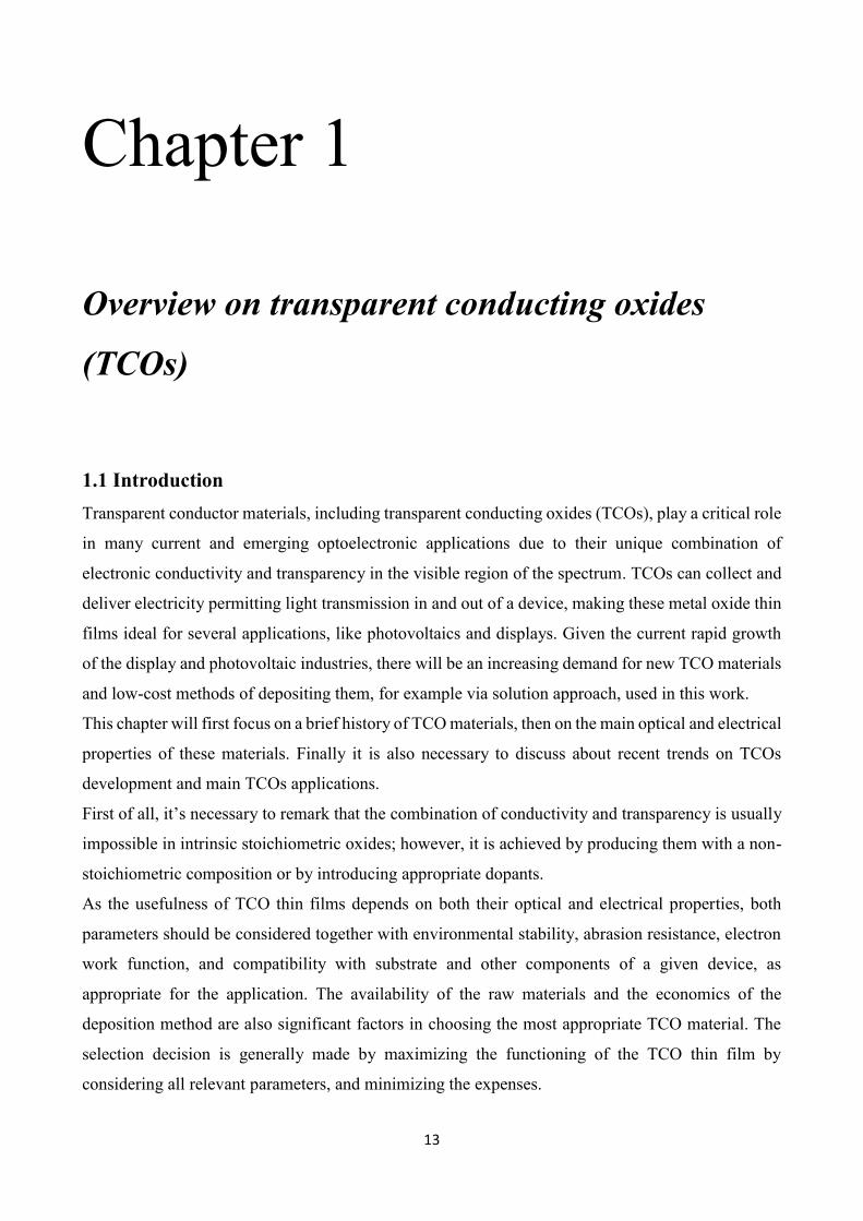
The minimum sample transmission (Tmin) in air can be expressed by:
(9)
Typical values of refractive index for TCO layers are n = 1.8 - 2.8. Assuming that, Tmin will be in the
range Tmin = 0.8 – 0.52. By decreasing the TCO film thickness, T is increased but the sheet resistance
decreases.
Figure 1.3 summarize some electrical and optical properties of different transparent conductive
materials. For flat-panel displays, the eye luminosity curve defines the requested spectral range,
whereas for thin-film solar cells the spectral irradiance from the Sun (under AM1.5 conditions), in
combination with the bandgap energy of the absorber material (such as silicon, CdTe or
Cu(In,Ga)Se2), sets the spectral limits for the transmittance of the layer. In the image in the left in
figure 1.3 are visible those spectra compared with optical transmittance of different TC materials.
2
min 2 2 2
4
(1 )( )
sub
sub
n nT
n n n
23
Figure 1.3 Optical transmittance T and sheet resistances Rs of transparent conductors materials. Bottom left: Spectral transmittance
of different TCE films: 12 Ω □–1, ITO (black); 10 Ω □–1, fluorine-doped SnO2 (green); 56 Ω □–1, single-walled carbon nanotubes (dashed
black); 23 Ω □–1, Ag nanowires (dotted blue); 50 Ω □–1, ZnO:Al (orange); and a low-emissivity coating 7 Ω □–1, SnO2/Ag/SnO2 (red).
Top Left: luminosity function of the human eye and spectral irradiance from the Sun under AM1.5 conditions. Right: Sheet resistance
Rs as a function of film thickness d for different TCE films: Ag, Al and Cu metal grids; PEDOT-PSS; ITO films; SWNTs; Ag nanogrid;
oxide/Ag/oxide films; and graphene.
The dependency of sheet resistance on film thickness is shown in the image in the right of Figure 1.3
for different types of transparent conductive materials. Most of the data follow the inverse
proportionality of sheet resistance Rs = ρfilm/d, which is expected for a thickness-independent
resistivity ρfilm. For comparison, calculated Rs curves for ρ = 10-5-10-2 Ω*cm are also plotted.
Graphene films exhibit the lowest resistivity (~5×10⁻⁶ Ω*cm), followed by TCO/Ag/TCO films and
Ag nanogrids (~5×10⁻⁵ Ω*cm). The plotted ITO data are somewhat high at ρITO ≈ 2-5×10⁻⁴ Ω*cm,
which is the lower range attainable by higher film thicknesses. The best ITO films today reach ρITO ≈
10-4 Ω*cm for d>100 nm, which would shift the ITO curve slightly to the left. PEDOT:PSS films and
Ag nanowire networks exhibit the highest resistivity.
1.3 Trend in development and main applications for transparent conductive
oxides
While the development of new TCO materials is mostly dictated by the requirements of specific
applications, low resistivity and low optical absorption are always significant prerequisites. There are
basically two strategies in managing the task of developing advanced TCOs that could satisfy the
applications requirements. The main strategy consists increasing the density of conducting electrons
through doping known binary TCOs with other elements.
For example, doping SnO2 with F- increase the carrier electron mobility by a factor of ~2 and their
concentration also by a factor of 2, reducing the resistivity by a factor of 4 [34]. The concentration of
F- dopant ions should not exceed an upper limit, as an increase in carrier scattering by F ions led to a
decrease in the conductivity. Doping SnO2 with Sb initially introduces Sb5+ ions that act as donors.
When the doping concentration was increased beyond a certain level, however, Sb3+ ions began to
replace the Sn4+ ions. The introduction of Sb3+ ions generates an acceptor level that compensates the
donors and increases the resistivity.
This effort to increase the conductivity without degrading the transparency was paralleled by a more
elaborate strategy in which two-binary and ternary TCOs were synthesized and characterized. The
two-binary systems include ZnO-SnO2, CdO-SnO2, and ZnO-In2O3. In spite of the expectations, the

24
electrical and optical properties of the two-binary TCOs were much inferior then those of ITO. The
phase diagram of the ternary TCOs could be schematically presented by a three-dimensional or four-
dimensional phase combination of the most common ternary TCO materials, based on known binary
TCO compounds [35]. Accordingly, the ternary TCO compounds could be formed by combining
ZnO, CdO, SnO2, In2O3 and GaO2 to obtain Zn2SnO4, ZnSnO3, CdSnO4, ZnGa2O4, GaInO3, Zn2In2O5,
Zn3In2O6, and Zn4In2O7. However, as Cd and its compounds are highly toxic, the utilization of these
TCOs is limited, though they have adequate electrical and optical properties. Other binary TCOs were
synthesized from known binary TCOs and also from non-TCO compounds, such as In6WO12 and the
p-type CuAlO2.
The first-principle model of Kiliç and Zunger [29], showed the importance of the composition in
turning an insulating oxide into a TCO. However, structural considerations should also be included.
Hosono et al. [36] investigated the conditions for depositing wide-gap amorphous oxides with high
electron mobility. They indicated that a large overlap between relevant orbitals is required. In
addition, the magnitude of the overlap needs to be insensitive to the structural randomness that is
intrinsic to the amorphous state. They assumed that since the spatial spreading of the ns orbital is
large and the overlap between these ns orbitals with spherical symmetry is large and insensitive to
any angular variations in the M-O-M bonds (where M is a metal cation) compared with p-p or d-p
orbitals having high anisotropy in geometry. Oxides composed of metal cations with an electronic
configuration (n-l)d10ns0 would satisfy these requirements, as the lowest part of the conduction band
in these oxides is primarily composed of ns orbitals. Hosono et al. [36] also conjectured that because
of this, ternary oxides are preferred to binary oxides for the formation of amorphous TCO thin films.
Scanning the periodic table, they identified 105 combinations of elements as promising ternary oxide
candidates.
Shannon et al. [37] conjectured that the formation of a transparent conductor could result from edge
sharing of Cd2+, In3+, and Sn4+ octahedra. Nearly all of the complex TCOs found to date possess
cations in octahedral coordination, as do most binary TCOs, with the exception of ZnO (wurtzite
structure) and -Ga2O3. These and other studies show that similar complex oxides may be a rich
source of new TCO materials [38, 39, 40].
All of the TCOs discussed above are n-type semiconductors. In addition, p-type doped TCOs were
also developed and could find interesting future applications, in particular in the new optoelectronic
field of transparent electronics [41]. Fabricating undoped or doped p-type TCOs was found to be
more difficult than the n-type. The first p-type TCO was made from CuAlO2 by Kawazoe [42] in
1997. Prior to this, however, in 1993 Sato et al. reported on a semi-transparent p-type TCO with ~40%
visible transmission [43]. It has been reported that is possible to form acceptor levels in ZnO, doping

25
with N, P and As. The difficulty in producing p-type oxide was hypothesized to result from the strong
localization of holes at oxygen 2p levels or due to the ionicity of the metallic atoms. O 2p levels are
far lower lying than the valence orbit of metallic atoms, leading to the formation of a deep acceptor
level with the holes. Hence, these holes are localized and require high energy to overcome a large
barrier height in order to migrate within the crystal lattice, resulting in poor hole-mobility and
conductivity [44] [45].
Growing p-ZnO was an important milestone in transparent electronics, allowing fabrication of wide
band gap p-n homo-junctions, which is a key structure in this field. It was anticipated that higher
conductivity and optical transmission could be obtained by doping ZnO with N, F, P, Sb, and As,
however, it was also shown that such doping had some serious limitations [46] [47]. Based on first
principle calculations, Yamamoto and Yoshida [48] proposed that co-doping of donor-acceptor
dopants (e.g. Ga and N, respectively) in ZnO might lead to p-type ZnO. Joseph et al. [49] applied this
principle to simultaneously dope ZnO with an acceptor (N) and a donor (Ga), where the acceptor
concentration was twice that of the donor. The optical transmission was greater than 85%, but the
conductivity was low, ~1 S/cm. P-type ZnO:Sb was deposited with a filtered vacuum arc equipped
with a Zn cathode doped by Sb. The conductivity was ~0.5 S/cm, the mobility 9-20 cm2/Vs and the
hole density ~4×1016 cm-3, with transmission of ~85%. It is evident that the challenge to grow p-type
TCO with resistivity of ~ 10-3 Ω*cm, or better, still exists.
Novel n-type transparent conductors were proposed using oxides with s2 electron configurations.
Oxides of Mg, Ca, Sc and Al also exhibited the desired optical and electronic features; however, they
have not been considered as candidates for achieving good electrical conductivity because of the
challenge of efficiently generating carriers in these wide band gap materials. The approach suggested
was to increase the mobility rather than the carrier density. If this goal could be achieved, the optical
properties would not deteriorate at lower resistivity. Recently, mobility with more than twice that of
commercial ITO was observed in Mo-doped In2O3 (IMO), and it was shown that the conductivity can
be significantly increased with no changes in the spectral transmittance upon doping with Mo [50].
Electronic band structure investigations of IMO by Medvedeva [51] revealed that the magnetic
interactions which had never been considered to play a role in combining optical transparency with
electrical conductivity ensure both high carrier mobility and low optical absorption in the visible
range. Recently, new thin film geometries were also explored in search of TCO films with higher
conductivity. A theoretical outline of a method to engineer high mobility TCOs was presented by
Robbins and Wolden [52], based on the high mobility transistor structure. The film should consist of
alternating thin layers of two semiconductors. One layer provides a high density of carriers, while the
second is a high mobility material. Electrons are supplied by the former and transported in the latter,

26
mitigating the limitations of ionized impurity scattering. The model of Robbins and Wolden assumes
that the electrons move into the high mobility material in response to differences in electron affinity.
However, the success of the proposed TCO design depends upon controlling the layer thickness at
nano dimensions, (e.g. ~5 nm). In addition, this approach depends on having materials of excellent
quality and compatible crystal structure in order to avoid problems related to interface defects.
To compare new and old materials performances, scientists began searching for a criterion that could
quantify and compare the properties of transparent conductors. In 1976, Haacke [53] provided a
simple measure that combines the transmittance T and the sheet resistance Rs of the layer to be
quantified, giving:
Φ𝐻 =𝑇𝑞
𝑅𝑠 = 𝑇𝑞𝜎𝑑 (11)
where q is an exponent that determines which transmittance is required for a specific purpose.
Exponents of q = 10, 20 or 100 lead to transmittances of 0.9, 0.95 or 0.99, respectively, for d = (αq)–
1, where α is the absorption coefficient. Usually, q = 10 is chosen because a transmittance of 0.9
(90%) is sufficient for most purposes.
In figure 1.4, a plot of Haacke’s figure of merit for different transparent conductive materials as a
function of film thickness, shows that TCO films yield a higher figure of merit than thin metal films.
The figure also shows that the original calculation for metal films underestimates the experimental
values of ΦH for a TCO/metal/TCO structure, thus giving figures of merit comparable to that of ITO
films. However, it is important to keep in mind that TCO/metal/TCO layer stacks exhibit a much
narrower spectral window than TCO films.
Figure 1.4 Figure of merit ΦH and transmittance T for different TC materials. a, ΦH as a function of film thickness d for metals (dotted
lines, left) and TCO layers (solid lines, right). b, Transmittance T in the visible range as a function of the sheet resistance Rs for
transparent conductor materials.
27
In recent years, another approach has also been used to compare different TCO materials [54], in
which the transmittance T in the visible wavelength range is displayed as a function of sheet resistance
Rs. According to theory, these dependences can be described by the formula [55, 56]:
𝑇 = 1/(1 +𝑍0𝜎𝑜𝑝𝑡
2𝑅𝑠𝜎𝑑.𝑐.) (12)
where Z0 is the vacuum impedance (Z0 = 1/ε0c = 377 Ω) and σopt and σd.c. are the optical and d.c.
conductivities of the material, respectively. T is typically measured in the visible range at a
wavelength of 550 nm, which corresponds to the maximum of the human eye luminosity curve.
According to equation 12, the ratio σd.c./σopt can be maximized for high transmittance at a particular
sheet resistance. This formula, although often used in literature, is not well substantiated; it is not
clear for which wavelength the optical conductivity σopt must be taken. Most experimental data for
T(Rs) have been reported for a wavelength of 550 nm. For nanowire and carbon nanotube networks,
for example, one must also take into account percolation in these films, which was recently pointed
out by De et al. [54].
Most of the transmittance curves are measured for transparent conductive materials on glass or plastic.
Although it is possible to measure the film transmittance and the uncoated substrate, a more rigorous
method would take into account the substrate with a refractive index nsub, giving, for d << λ/2πnfilm
with a wavelength λ and refractive index nfilm [57]:
𝑇 = 16𝑛𝑠𝑢𝑏
2
(1+𝑛𝑠𝑢𝑏)4
1
[1+𝑍0𝑅𝑠
1
(1+𝑛𝑠𝑢𝑏)
𝜎𝑜𝑝𝑡
𝜎𝑑.𝑐.]2
(13)
Equation 12 and equation 13 were both used to fit the data in Figure?. The large scattering of the data
points is due to the different materials and preparation procedures. The main fit parameter (besides
nsub) is the ratio σd.c./σopt, which is highest for metal structures (films and nanowires) and ITO films,
slightly lower for graphene films, and lowest for single-walled carbon nanotubes. This can also be
inferred from figure 1.4, in which ITO, graphene and Ag grids are the materials that fit best to the
target application (the dashed rectangle). Most of these data are given for T(550 nm); that is, at the
maximum of the eye luminosity function. For transparent conductor materials applications in thin-
film solar cells, a better measure for the transmittance would be the average of T over the spectral
range of 400–1000 nm, or a weighted transmittance that takes into account the spectral irradiance of
the sun and bandgap energy of the specific solar absorber. In summary, this semi-empirical T(Rs)
relation can be used to judge thin-film TCE materials for a prospective application. Attaining a better
28
fundamental understanding requires a firm theoretical analysis of the optical conductivity σopt based
on density functional theory calculations beyond the well-known Drude theory.
TCOs have several industrial applications. TCO coatings are applied to transparent materials used for
work surfaces and closet doors, particularly in clean rooms used for electronics assembly, in order to
prevent harmful static charges. In this application relatively high surface resistances (e.g. k/) can
be tolerated.
Transparent heating elements may be TCOs coatings. These are applied as defrosters in aircraft and
vehicular windshields. Their advantage over traditional hot air blowers is that they can have a much
shorter effective defrosting time, and work uniformly over large areas. This application requires either
the use of very low surface resistance coatings (e.g. ~1 /), or a high voltage power source. The
application of TCO coatings to passenger vehicles has proven to be technically successful but a
commercial failure, due to the high cost of a supplemental alternator to deliver the requisite high
voltage. If the automobile industry will adopt a higher bus voltage, as has been widely discussed, then
this application may prove to be more commercially feasible in the future.
TCO coatings may be used as shielding to decrease electromagnetic radiation interference from
providing visual access. This may be either to keep radiation from escaping an enclosure, to avoid
interfering with nearby devices, or from entering an enclosure to prevent external radiation sources
from interfering with electronic devices within. One potential example is the window of domestic
microwave ovens, which today use a perforated metal screen, which obscures clear visual
observation, to reduce microwave leakage. Radiation leakage must be minimized to prevent harm to
the users, as well as interference to proliferating wireless devices which use the unlicensed spectral
band at 2.45 GHz. While transparent conducting films were proposed 50 years ago, an attempt to
introduce microwave windows with TCO coatings into the market was not successful about a decade
ago, due to the high cost. Low cost designs are currently being developed. The three largest
applications of transparent conductive oxide thin films, in terms of the surface area covered, and their
total value, are flat panel displays, solar cells, and coatings on architectural glass. In general,
transparent electrodes are needed for a large variety of electro-optical devices, of which flat panel
displays and solar cells are the most important examples.
In liquid crystal displays (LCDs), TCO films are needed for both electrodes, in order to allow
backlighting to pass through the liquid crystal film while applying voltage to the various pixels.
Generally these electrodes are in the form of a pattern of lines, with the alignment of the lines on the
two electrodes perpendicular to each other. This allows addressing individual pixels by applying a
voltage to the two lines which intersect at a given pixel. Thus patterning the films is required. ITO is
the TCO of choice in this application, both because of its electro-optical properties, and the relative

29
ease of acid etching. The best LCDs utilize an active matrix comprising one amorphous silicon
transistor which occupies a corner of each pixel, and because the silicon is opaque, has reduced light
transmission. Recently transparent field effect transistors (FETs) have been developed based on the
zinc oxide, but using a Cr gate. These zinc oxide FETs have been incorporated into small 220X280
10 m pixel active matrix LCDs [58]. Small and medium LCDs are a 25 B$/yr market which is
growing by about 5%/yr, while large area LCDs have a similar market size and a much higher growth.
The explosive growth for demand of ITO coatings for this specific application has generated wide
spread concern about Indium scarcity in the near future.
Most solar cells use TCO films as a transparent electrode. Major considerations in the choice of the
TCO for this application, besides the conductivity and transparency, are electronic compatibility with
adjacent layers in the cell, processing requirements, and stability under environmental conditions.
Often tin oxide based films are chosen for this application, in as much as patterning is not required,
but environmental stability is. TCO films are commonly applied to architectural glass, often as part
of multi-layer stacks. In window glass applications, usually the conductivity per se is irrelevant, but
rather the concurrent high infrared reflectivity is exploited, in order to obtain good light transmission
in the visible range, while minimizing heat transmission. This feature is used to minimize air
conditioning costs in the summer, and heating costs in the winter, in buildings equipped with
appropriately coated windows. Approximately 25% of flat glass is coated, and energy conserving
coatings are now mandatory in various regions. Most commonly the coatings are applied by two
techniques. (1) Very enduring and inexpensive, but simple, coatings are produced with atmospheric
pressure chemical vapor deposition (APCVD), in line with the float glass production process. This
insures a fresh surface, and exploits the high temperature of the glass during its production. However,
APCVD is not very flexible and there are only limited options available for the coating architecture.
(2) A more flexible, but also more costly, process is magnetron sputtering. Commonly multiple (e.g.
20-60) rotary targets are mounted in long modular vacuum systems (e.g. 40-160 m length), and
multilayer stacks are deposited as the glass panels pass beneath the various cathodes, traveling at
velocities of ~1 m/s. Typically these systems operate continuously for 2 weeks, after which expended
targets are replaced and other maintenance is performed. The expanding use of TCO materials,
especially for the production of transparent electrodes for optoelectronic device applications, has
developed into a worldwide multi-billion $US economy that in general depends on the availability of
ITO.
Concluding, the situation drives the search for alternative TCO materials to replace ITO, and
motivates an intensive investigation of the physics and chemistry of TCO materials. The main
significant progress in the research and development of TCO thin films has been made in
30
understanding the physics of TCO semiconductors. The physical processes that make possible the
coexistence of electrical conductivity and optical transparency are well clarified and understood. In
particular, the role of oxygen vacancies and various dopants in the formation of shallow donor levels
is well established. In addition to binary TCOs, progress has also been made in developing new TCO
compounds, consisting of combined segregated-binaries, ternary and quaternary oxides. However,
the objective of developing new TCOs with conductivity similar or even higher than that of ITO has
not been realized. The conductivity of the recently developed ternary, quaternary, and binary-
combination TCOs is lower than that of ITO. It is now appreciated that the attainment of higher
conductivity is limited by the negative correlation between carrier density and electron mobility. It is
now realized that the development of TCOs with higher conductivity does not necessarily depend on
higher dopant concentration that provides higher carrier density, but could also be achieved by
maintaining moderate carrier density with increased mobility. These wide band gap oxides exhibited
the desired optical and electronic features; however, their conduction was too low. p-type TCOs were
obtained by doping ZnO with N, F, P, Sb, and As, however, it was also shown that such doping had
some serious limitations, and the conductivity was lower than n-type ZnO. In summary, AZO, GZO
and FTO are at present the only TCOs with electrical conductivity close to that of ITO, and with
appropriate high optical transmission in the near-UV, VIS and NIR. The objective of producing TCO
materials with optical and electrical characteristics equivalent to those of ITO is the main aim of the
present thesis.

31
References
[1] Bädeker, K. Über die elektrische Leitfähigkeit und die thermoelektrische Kraft einiger
Schwermetallverbindungen. Ann. Phys. 22, 749–766, 1907
[2] Preston, J. S. Constitution and mechanism of the selenium rectifier photocell. Proc. R. Soc. Lond.
A 202, 449–466 (1950).
[3] McMaster, H. A. Electrically conducting films and method of application. UK patent 1947
[4] Hutson, A. R. Piezoelectricity and conductivity in ZnO and CdS. Phys. Rev. Lett. 4, 505–507 1960
[5] van Boort, H. J. J. & Groth, R. Low-pressure sodium lamps with indium oxide filters. Phil. Tech.
Rev. 29, 47–48 1968
[6] Köstlin, H., Jost, R. & Lems, W. Optical and electrical properties of doped In2O3 films. Phys. Stat.
Sol. A 29, 87–93 1975
[7] White, D. L. & Feldman, M. Liquid-crystal light valves. Electron. Lett. 6, 837–839 1970
[8] Lampert, C. M. Heat mirror coatings for energy conserving windows. Sol. Energ. Mat. 6, 1–41
1981
[9] Hamberg, I. & Granqvist, C. G. Evaporated Sn-doped In2O3 films: basic optical properties and
applications to energy-efficient windows. J. Appl. Phys. 60, R123–R159 1986
[10] Szczyrbowski, J., Bräuer, G., Ruske, M., Schilling, H. & Zmelty, A. New low emissivity coating
based on TwinMag sputtered TiO2 and Si3N4 layers. Thin Solid Films 351, 254–259 1999
[11] Grosse, P., Hertling, R. & Müggenburg, T. Design of low emissivity systems based on a three-
layer coating. J. Non-Cryst. Solids 218, 38–43 1997
[12] Riedel, S., Röber, J. & Geßner, T. Electrical properties of copper films produced by MOCVD.
Microelectr. Eng. 33, 165–172 1997
[13] Granqvist, C. G. Transparent conductors for solar energy and energy efficiency: a broad-brush
picture. Int. J. Nanotech. 6, 785–798 2009
[14] Betz, U., Olsson, M. K., Marthy, J., Escola, M. F. & Atamny, F. Thin films engineering of indium
tin oxide: large area flat panel displays application. Surf. Coat. Techn. 200, 5751–5759 2006
[15] Katayama, M. TFT-LCD technology. Thin Solid Films 341, 140–147 1999
32
[16] Chopra, K. L., Major, S. & Pandya, D. K. Transparent conductors: a status review. Thin Solid Films
102, 1–46 1983
[17] Klenk, R. in Transparent Conductive Zinc Oxide: Basics and Application in Thin Film Solar Cells
(eds Ellmer, K., Klein, A. & Rech, B.) Ch 9, Springer, 2008
[18] R. G. Gordon, MRS Bull., 2000, 25, 52–57
[19] Robert M. Pasquarelli, David S. Ginley, Ryan O’Hayrea, Solution processing of transparent
conductors: from flask to film, Chem. Soc. Rev., 2011, 40, 5406–5441
[20] David Mitzi, Solution Processing of Inorganic Materials, John Wiley and Sons, 2009.
[21] Kalowekamo, J., Baker, E., Estimating the manufacturing cost of purely organic solar cells, Sol.
Energy, 2009
[22] CRC Handbook of Chemistry and Physics, 2005.
[23] A. J. Leenheer, J. D. Perkins, M. F. A. M. van Hest, J. J. Berry, R. P. O’Hayre and D. S. Ginley,
General mobility and carrier concentration relationship in transparent amorphous indium zinc oxide
films, Phys. Rev. B, 2008, 77, 115215
[24] R. E. Hummel, Electronic Properties of Materials, Springer- Verlag, New York, 3rd edn, 2001
[25] Enrico Della Gaspera, Marco Bersani, Michela Cittadini, Massimo Guglielmi, Diego Pagani,
Rodrigo Noriega, Saahil Mehra, Alberto Salleo, and Alessandro Martucci, J. Am. Chem. Soc., 2013,
135 (9), pp 3439–3448
[26] T. O. Mason, G. B. Gonzalez, D. R. Kammler, N. Mansourian-Hadavi and B. J. Ingram, Proceedings
of the 2nd International Symposium on Transparent Oxide Thin Films for electronics and Optics, Thin
Solid Films, 2002, 411, 106–114.
[27] J. W. Fergus, Doping and defect association in oxides for use in oxygen sensors, J. Mater. Sci.,
2003, 38, 4259–4270.
[28] C.G. Van de Walle, Hydrogen as a cause of doping in Zinc Oxide, Phys. Rev. Lett., 85, 1012, 2000.
[29] C. Kiliç and A. Zunger, Origins of coexistence of conductivity and transparency in SnO2, Phys.
Rev. Lett., 88, 095501-1, 2002
[30] B. Thangaraju, Thin Solid Films, 402, 71, 2002
[31] Ellmer, K. Resistivity of polycrystalline zinc oxide films: current status and physical limit, J. Phys.
D: Appl. Phys. 34, 3097–3108 2001
[32] C. Kittel, Introduction to Solid State Physics, John Wiley and Sons, New York, 7th edn, 1996.
[33] H. Agura and H. Suzuki, T. Matsushita, T. Aoki, and M. Okuda, Thin Solid Films, 445, 263 2003
[34] E. Shanthi, A. Banerjee, V. Dutta, and K.L. Chopra, J. Appl. Phys., 53, 1615 1982

33
[35] A. Kurz, K. Brakecha, J. Puetz, and M. A. Aegerter, Thin Solid Films, 502, 212 2006
[36] H.Hosono, M. Yasukawa, H. Kawazoe, Novel oxide amorphous semiconductors, J. Non-Cryst.
Solids, 203, 334, 1996
[37] R.D. Shannon, J.L. Gilson, R.J. Bouchard, J. Phys. Chem. Solids, 38, 877, 1977
[38] H. Kawazoe, N. Ueda, H. Un’no, T. Omata,H. Hosono, H. Tanoue, J. Appl. Phys., 76, 7935 1994
[39] R. J. Cava, J. M. Phillips, J. Kwo, G.A. Thomas, R.B. van Dover,S.A. Carter,J.J. Krajewski, W.F.
Peck Jr., J.H. Marshall, D.H. Rapkine, Appl. Phys. Lett., 64, 2071, 1994
[40] T. Minami, Mater. Res. Soc. Bull., 25, 38, 2000
[41] A.N. Banerjee and K.K. Chattopadhyay, Progress in Crystal Growth and Characterization of
Materials, 50, 52, 2005
[42] H. Kawazoe, Nature, 389, 939, 1997
[43] H. Sato, T. Minami, S. Takata, and T. Yamada, Thin Solid Films 236, 27, 1993
[44] H. Kawazoe, H. Yanagi, K. Ueda, H. Hosono, MRS Bull. 28, 2000
[45] S. Fraga, S. Karwowski, K.M.S. Saxena, Handbook of Atomic Data, Elsevier, Amsterdam, 1976
[46] S.J. Pearton, D.P. Norton, K. Ip, Y.W. Heo, and T. Steiner, Progress in Materials Science 50, 293,
2005
[47] S. B. Zhang, S-H Wei, and A. Zunger, J. Appl. Phys., 83, 3192, 1998
[48] T. Yamamoto and H.K. Yoshida, Jpn. J. Appl. Phys. 38, L166, 1999
[49] M. Joseph, H. Tabata, and T. Kawai, Jpn. J. Appl. Phys. 38 L1505, 1999
[50] Y. Yoshida, D.M. Wood, T.A. Gessert, and T.J. Coutts, Appl. Phys. Lett. 84, 2097, 2004
[51] J.E. Medvedeva, Phys. Rev. Lett. 97, 086 401, 2006
[52] J.J. Robins and C.A. Wolden, Appl. Phys. Lett., 83, 3933, 2003
[53] Haacke, G. New figure of merit for transparent conductors. J. Appl. Phys. 47, 4086–4089 1976
[54] De, S., King, P. J., Lyons, P. E., Khan, U. & Coleman, J. N. Size effects and the problem with
percolation in nanostructured transparent conductors. ACS Nano 4, 7064–7072 2010
[55] Glover, R. E. & Tinkham, M. Conductivity of superconducting films for photon energies
between 0.3 and 40 kTc. Phys. Rev. 108, 243–256 1957
[56] Dressel, M. & Grüner, G. Electrodynamics of Solids Ch 8 (Cambridge Univ., 2002).
[57] Barnes, T. M. et al. Comparing the fundamental physics and device performance of transparent,
conductive nanostructred networks with conventional transparent oxides. Adv. Energ. Mat. 2, 353–
360 2012

34
[58] T. Hirao, M. Furuta, T. Hiramtsu, “ZnO-based TFT for use in LCD” 35th Int. Conf on Metallurgical
Coatings and Thin Films, San Diego, 28 April-2 May 2008.

35
Chapter 2
Colloidal synthesis of metal and metal oxide
nanoparticles
2.1 Introduction
This chapter will focus on colloidal nanoparticles synthesis theory. First of all, a brief introduction of
colloidal nanoparticles is presented; then the nanocrystals formation mechanism. Finally, brief
digressions about synthesis of heat up “non-injection” synthesis are also discussed.
Nanocrystals discussed here are tiny crystals of metals or semiconductors material consisting of
hundreds to a few thousand atoms. What is special about the size regime of these nanoparticles? The
coupling of over hundreds to thousands atoms is necessary to develop the band structure of metals,
semiconductors, and magnetic materials. In the nanoscale regime, the electronic structure, optical,
and magnetic properties of materials can be tuned by varying the physical size of the crystal, leading
to new phenomena, such as superparamagnetism of magnetic NCs, surface plasmon resonance in Au
and Ag nanoparticles [1], and the size dependent band gap of semiconductor NCs [2], [3]. This
behavior opens interesting opportunities for several device applications.
Inorganic semiconductors have a proven track record in electronics and optoelectronics; they offer
superior carrier mobilities, light absorption, photo, and thermal stability. However, they are difficult
to form by low cost processes. Crystallization of inorganic semiconductors requires high temperature
treatments, which force trade-offs between device performance, fabrication costs, and compatibility
with flexible plastic substrates. The development of applications ranging from photovoltaics to light-
emitting devices, radio frequency tags, and sensors could be accelerated by introducing lower cost
alternatives to conventional technologies that rely on single crystals [4]. Here, the nanometer size
crystals can find commercial use as the building blocks for inexpensive manufacturing of low cost
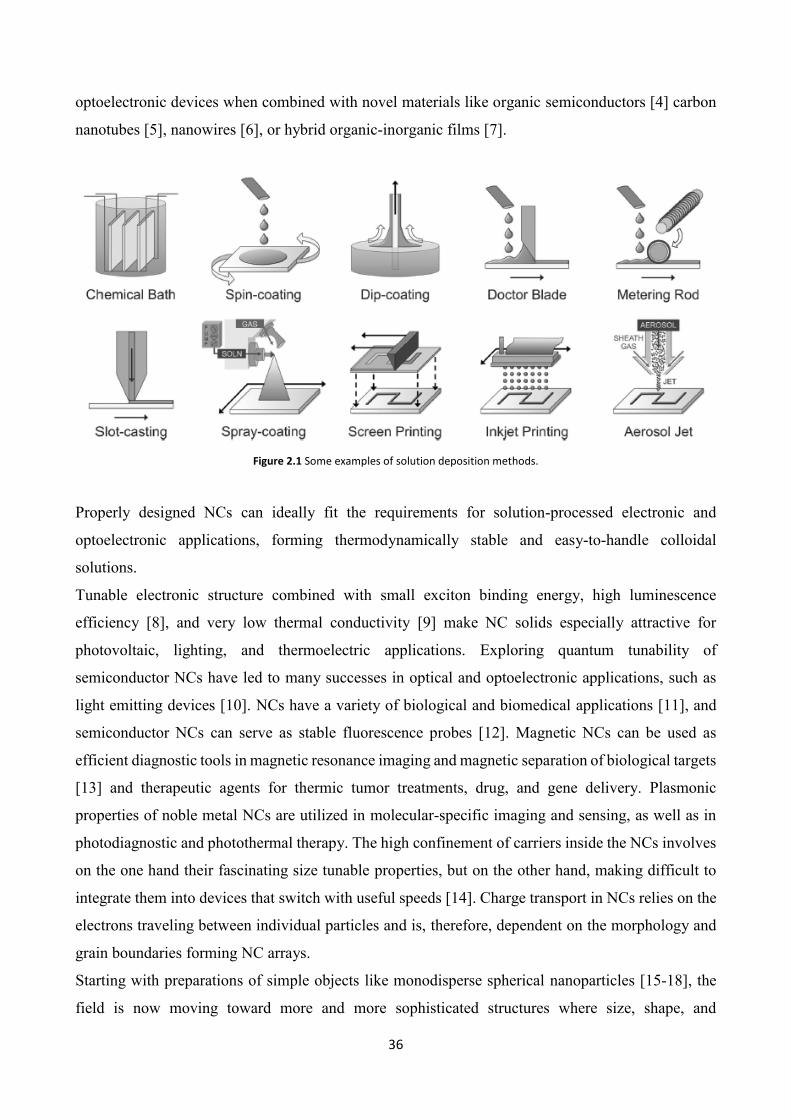
and large area devices. Solution-based deposition processes, such as spin coating, dip coating, or
inkjet printing, (see figure 2.1) offer substantial cost reductions for the fabrication of electronic and
36
optoelectronic devices when combined with novel materials like organic semiconductors [4] carbon
nanotubes [5], nanowires [6], or hybrid organic-inorganic films [7].
Figure 2.1 Some examples of solution deposition methods.
Properly designed NCs can ideally fit the requirements for solution-processed electronic and
optoelectronic applications, forming thermodynamically stable and easy-to-handle colloidal
solutions.
Tunable electronic structure combined with small exciton binding energy, high luminescence
efficiency [8], and very low thermal conductivity [9] make NC solids especially attractive for
photovoltaic, lighting, and thermoelectric applications. Exploring quantum tunability of
semiconductor NCs have led to many successes in optical and optoelectronic applications, such as
light emitting devices [10]. NCs have a variety of biological and biomedical applications [11], and
semiconductor NCs can serve as stable fluorescence probes [12]. Magnetic NCs can be used as
efficient diagnostic tools in magnetic resonance imaging and magnetic separation of biological targets
[13] and therapeutic agents for thermic tumor treatments, drug, and gene delivery. Plasmonic
properties of noble metal NCs are utilized in molecular-specific imaging and sensing, as well as in
photodiagnostic and photothermal therapy. The high confinement of carriers inside the NCs involves
on the one hand their fascinating size tunable properties, but on the other hand, making difficult to
integrate them into devices that switch with useful speeds [14]. Charge transport in NCs relies on the
electrons traveling between individual particles and is, therefore, dependent on the morphology and
grain boundaries forming NC arrays.
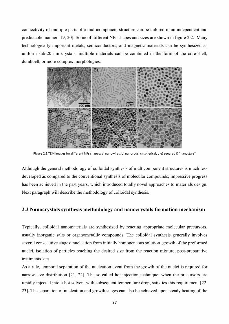
Starting with preparations of simple objects like monodisperse spherical nanoparticles [15-18], the
field is now moving toward more and more sophisticated structures where size, shape, and
37
connectivity of multiple parts of a multicomponent structure can be tailored in an independent and
predictable manner [19, 20]. Some of different NPs shapes and sizes are shown in figure 2.2. Many
technologically important metals, semiconductors, and magnetic materials can be synthesized as
uniform sub-20 nm crystals; multiple materials can be combined in the form of the core-shell,
dumbbell, or more complex morphologies.
Figure 2.2 TEM images for different NPs shapes: a) nanowires, b) nanorods, c) spherical, d,e) squared f) “nanostars”
Although the general methodology of colloidal synthesis of multicomponent structures is much less
developed as compared to the conventional synthesis of molecular compounds, impressive progress
has been achieved in the past years, which introduced totally novel approaches to materials design.
Next paragraph will describe the methodology of colloidal synthesis.
2.2 Nanocrystals synthesis methodology and nanocrystals formation mechanism
Typically, colloidal nanomaterials are synthesized by reacting appropriate molecular precursors,
usually inorganic salts or organometallic compounds. The colloidal synthesis generally involves
several consecutive stages: nucleation from initially homogeneous solution, growth of the preformed
nuclei, isolation of particles reaching the desired size from the reaction mixture, post-preparative
treatments, etc.
As a rule, temporal separation of the nucleation event from the growth of the nuclei is required for
narrow size distribution [21, 22]. The so-called hot-injection technique, when the precursors are
rapidly injected into a hot solvent with subsequent temperature drop, satisfies this requirement [22,
23]. The separation of nucleation and growth stages can also be achieved upon steady heating of the

38
reaction mixture [24]. Nucleation and growth of NCs occurs in the solution phase in the presence of
organic surfactant molecules, which dynamically adhere to the surface of growing crystals [24].
Typical surfactants include long-chain carboxylic and phosphonic acids (e.g., oleic acid and n-
octadecylphosphonic acid), alkanethiols (e.g., dodecanethiol), alkyl phosphines, alkylphosphine
oxides (classical examples are trioctylphosphine, TOP, and trioctylphosphine oxide, TOPO), and
alkylamines such as hexadecylmine. The surfactant molecules play the key role in tuning the kinetics
of nucleation and growth [25, 26] which should be kinetically balanced because if the nanoparticle
nucleation rate is either too slow or too fast with respect to the growth rate, the reaction will
generaterespectively bulk crystals or molecular clusters. Achieving proper balance of these
intrinsically different processes is an important and sometimes challenging problem, which is usually
addressed empirically by searching for a good combination of molecular precursors, surfactants,
solvent, and the reaction conditions (temperature regime, etc.).
Development of reproducible synthetic approaches leading to nanoparticles with uniform size, shape,
composition, and surface morphology is extremely important for further progress in fundamental
studies and practical applications. In figure 2.3 are presented several examples of metal nanocrystals
synthesized by colloidal chemistry.
Figure 2.3 TEM images of different metal nanoparticles (Au, Ag, Pd, Bi, CoPt3, FePt)
39
Metal nanoparticles can be easily synthesized by reducing the metal ions using reductant such as
borohydride, amines, or 1,2-diols in the presence of stabilizing agents, typically long-chain
alkanethiols (e.g., dodecanethiol), amines, or fatty acids. This approach works quite well for noble
metals [27, 28] and their alloys [29]. Current developments in the synthesis of these materials have
been extensively reviewed by Yang et al. [30] and Liz-Marzan [31].
More reactive transition and main group metals like Cobalt, Iron, Crome [32, 33] require rigorous
control of the reaction conditions and are synthesized under inert atmosphere. High temperatures, up
to 300 °C, are often necessary to anneal out the defects in crystalline lattice and form highly crystalline
particles [26]. High boiling solvents are used to provide a wide window of reaction temperatures. The
choice of solvent limits the range of possible molecular precursors. For example, solvents with low
polarity such as dioctyl ether or 1-octadecene require precursors soluble in this medium. Among metal
salts, acetylacetonates or carboxylates are frequently used [16, 26] in the synthesis of metal
nanoparticles.
Alternatively, metal NCs can be generated by thermal decomposition of molecules containing
zerovalent metal, such as metal carbonyls. For example, cobalt nanoparticles can be synthesized
either by reduction of Co(II) ions in solution or by thermal decomposition of Co2(CO)8. Longchain
carboxylic acids or alkylamines are the typical surfactants for metal NCs. In addition to size and
shape, precursors and surfactants can control the crystalline phase of the nanoparticle. Thus, three
different polymorphs of cobalt NCs (hexagonal close-packed, face-centered cubic, and epsilon phase)
were selectively synthesized by adjusting reaction parameters [26]. Combining two or more metal
precursors, for example, Pt(acac)2 and Fe(CO)5, in a one-pot reaction allows one to obtain
nanoparticles of metal alloys [16, 26]. Among a variety of possible metal combinations, the alloys of
magnetic metals (Fe, Co, and Ni) with Pt and Pd have been studied most extensively because in these
systems alloying helped to overcome a serious drawback of elemental magnetic nanoparticles, their
low stability against oxidation.
Several methods can be used to tune the size of metal nanoparticles during synthesis. Usually, the
metal nanoparticles nucleate and grow very quickly, and it is difficult to terminate the reaction at the
desired stage of particle growth. Instead, the particle size can be adjusted by first making small
nanoparticles, which are then used as seeds for further growth by adding controllable amounts of
molecular precursors. For example, this method was applied to vary the size of FePt NCs [16].
Another approach is based on tuning the relative rates of nanoparticle nucleation and growth. If the
total amount of molecular precursors used in the reaction is constant, the fast nucleation provides
high concentration of nuclei and yields smaller NCs. Instead, slow nucleation provides low
40
concentration of seeds consuming the same amount of precursors, thus resulting in larger particles
[26].
The balance between nucleation and growth rates can be tuned via changing of the reaction
temperature because the activation energy for the homogeneous nucleation is usually much higher
than that for particle growth [34]. Typically, the increase of reaction temperature allowed one to
obtain smaller NCs for different materials [26]. Besides the reaction temperature, there are a number
of other methods to control particle size, such as nature and concentration of capping molecules,
molar ratios of precursors, etc.
Significant success was achieved in the synthesis of NCs of different technologically important
semiconductors, for example for the synthesis of II-VI (CdSe, CdTe, CdS) [35, 36], III-V (InP, InAs)
[37, 38] and IV-VI (PbS, PbSe, PbTe [39]) semiconductor. The syntheses are carried out at high
temperatures, and in the presence of long-chain alkylphosphines (e.g., trioctylphosphine, TOP),
alkylphosphine oxides (e.g., trioctylphosphine oxide, TOPO), alkylamines (e.g., hexadecylamine,
HDA), and alkylphosphonic acids as the stabilizing agents. In many cases, the size of semiconductor
NCs can be tuned by adjusting the concentrations of surfactants, reaction temperature, and duration
of the particle growth. In a colloidal solution, semiconductor NCs often grow through the Ostwald
ripening mechanism, where the largest particles in solution grow at the expense of dissolving smaller
ones.
As a result, average particle size increases with time [34], and the particle concentration decreases. A
number of studies investigated the kinetics of nanoparticle growth and dissolution to model this self-
consistent growth process and understand the parameters that control particle size distribution during
the synthesis of semiconductor NCs [38]. Two regimes, so-called “focusing” and “defocusing” of
size distribution during nanoparticle growth, were described by Peng et al. [40, 41].
Ostwald ripening model was proposed to describe the evolution of an ensemble of nanoscale particles
[42]. Tuning particle size and controlling surface chemistry open possibility to eliminate the midgap
states associated with surface dangling bonds. As a result of reduced probability of carrier trapping
and nonradiative recombination, high (>80%) luminescence quantum efficiencies were achieved for
semiconductor NCs [43, 44].
Discussion of solution-phase synthesis of inorganic nanomaterials would be incomplete without
mentioning other methodologies, complementary to above-described high temperature synthesis in
nonpolar organic solvents. Thus, there are several examples of high-quality semiconductor
nanoparticles synthesized in aqueous medium [45, 46]. Generally, the NCs made in aqueous medium
are not as monodisperse as those prepared in organic solvents, but in other aspects, such as
luminescence efficiency, colloidal stability, and, especially, cost per gram, they can be very

41
competitive. The other prominent methodology is the so-called sol-gel technique that has been widely
studied as one of the most popular routes for synthesis of oxide materials [47, 48]. Typical precursors
for sol-gel process are metal alkoxides and metal chlorides, which undergo hydrolysis and
polycondensation reactions to form a colloid. Traditional sol-gel processes include a series of
hydrolysis and condensation reactions of the precursors in acidic or basic aqueous or alcohol media,
forming first nanoparticles (colloidal sols) controllably aggregating into a wet network (gel). The sol-
gel process can be divided into several stages: (i) formation of stable solutions of the metal alkoxide
(the sol); (ii) gelation resulting from the formation of an oxide- or alcohol-bridged network by a
polycondensation reaction (the gel); (iii) aging of the gel (syneresis) accompanied by contraction of
the gel network and expulsion of solvent from the gel pores; (iv) drying to remove water and other
volatile liquids from the gel network; (v) dehydration for removing surface-bound M-OH groups; and
(vi) thermal decomposition of the gels at high temperatures. From this process, the pores of the gel
network are collapsed, and the remaining organic precursors are decomposed. Depending upon how
the wet gel is dried, the density and extent of porosity of the network can be effectively tuned,
consequently impacting the bulk physical properties. Solvent removal can have a huge effect on the
gel structure and is a critical step for creating nanostructures with desired functionality [49]. During
thermal drying or room-temperature solvent evaporation, capillary forces induce stresses on the gel
that induce collapse of the network, eventually leading to so-called xerogels with a collapsed but still
porous form of the original gel network. On the other hand, the supercritical extraction of solvent
from a gel does not induce capillary stresses due to the lack of solvent-vapor interfaces [49].
In analogy with bulk crystals, the nanoparticles are terminated by facets that expose different
crystallographic planes. Selective adhesion of surfactant molecules allows for tuning the growth
kinetics of different crystal facets and tailoring the NC shape from nearly spherical to highly
anisotropic [19]. Strong binding of capping molecules suppresses the growth of certain facets, leading
to a variety of NC shapes. The multicomponent mixtures of stabilizing agents are often employed to
provide the difference in growth rate in different crystallographic directions. For example, depending
on the length of alkyl chain and concentration of alkylphosphonic acid and the heating regime, the
rod-, arrow-, rise-, teardrop-, and tetrapod-shaped CdSe NCs can be synthesized [4]. Possible
nanoparticle shapes are determined by symmetry of underlying crystal lattice; for example, PbSe NCs
with rocksalt atomic lattice can be synthesized in the form of spheres, cubes, octahedrons, or
starshaped NCs [20]. Tetrapods of ZnO [50], iron oxide [51], Pt [52], CdSe [53, 54], CdTe [55] are
examples of nanomaterials with higher level of morphological complexity. There are a number of
other techniques that can be applied to engineer the shape of colloidal NCs. Thus, long uniform
colloidal nanowires can be synthesized by the oriented attachment [56, 57] or solution-liquid-solid
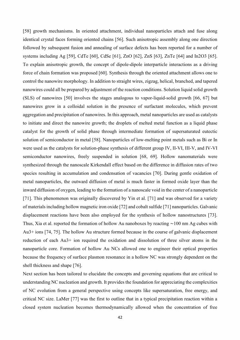
42
[58] growth mechanisms. In oriented attachment, individual nanoparticles attach and fuse along
identical crystal faces forming oriented chains [56]. Such anisotropic assembly along one direction
followed by subsequent fusion and annealing of surface defects has been reported for a number of
systems including Ag [59], CdTe [60], CdSe [61], ZnO [62], ZnS [63], ZnTe [64] and In2O3 [65].
To explain anisotropic growth, the concept of dipole-dipole interparticle interactions as a driving
force of chain formation was proposed [60]. Synthesis through the oriented attachment allows one to
control the nanowire morphology. In addition to straight wires, zigzag, helical, branched, and tapered
nanowires could all be prepared by adjustment of the reaction conditions. Solution liquid solid growth
(SLS) of nanowires [50] involves the stages analogous to vapor-liquid-solid growth [66, 67] but
nanowires grow in a colloidal solution in the presence of surfactant molecules, which prevent
aggregation and precipitation of nanowires. In this approach, metal nanoparticles are used as catalysts
to initiate and direct the nanowire growth; the droplets of melted metal function as a liquid phase
catalyst for the growth of solid phase through intermediate formation of supersaturated eutectic
solution of semiconductor in metal [58]. Nanoparticles of low-melting point metals such as Bi or In
were used as the catalysts for solution-phase synthesis of different group IV, II-VI, III-V, and IV-VI
semiconductor nanowires, freely suspended in solution [68, 69]. Hollow nanomaterials were
synthesized through the nanoscale Kirkendall effect based on the difference in diffusion rates of two
species resulting in accumulation and condensation of vacancies [70]. During gentle oxidation of
metal nanoparticles, the outward diffusion of metal is much faster in formed oxide layer than the
inward diffusion of oxygen, leading to the formation of a nanoscale void in the center of a nanoparticle
[71]. This phenomenon was originally discovered by Yin et al. [71] and was observed for a variety
of materials including hollow magnetic iron oxide [72] and cobalt sulfide [71] nanoparticles. Galvanic
displacement reactions have been also employed for the synthesis of hollow nanostructures [73].
Thus, Xia et al. reported the formation of hollow Au nanoboxes by reacting ∼100 nm Ag cubes with
Au3+ ions [74, 75]. The hollow Au structure formed because in the course of galvanic displacement
reduction of each Au3+ ion required the oxidation and dissolution of three silver atoms in the
nanoparticle core. Formation of hollow Au NCs allowed one to engineer their optical properties
because the frequency of surface plasmon resonance in a hollow NC was strongly dependent on the
shell thickness and shape [76].
Next section has been tailored to elucidate the concepts and governing equations that are critical to
understanding NC nucleation and growth. It provides the foundation for appreciating the complexities
of NC evolution from a general perspective using concepts like supersaturation, free energy, and
critical NC size. LaMer [77] was the first to outline that in a typical precipitation reaction within a
closed system nucleation becomes thermodynamically allowed when the concentration of free

43
monomer, [M], is raised above a critical (nucleation) concentration, [MC]. At this point the solution
is supersaturated. As monomer is rapidly consumed during the nucleation event, the concentration of
free monomer eventually drops below [MC] and nucleation ceases. For newly formed nuclei with a
radius a, [M] is still well above its equilibrium monomer concentration, [Ma] (concentration of
monomer required to prevent the dissolution of particles with r ≥ a), upon the cessation of nucleation.
As such, all particles with r > a will grow through the accretion of monomer. Although [M] is still
well above [M∞] (the concentration of monomer in equilibrium with a flat surface), as monomer is
consumed throughout the reaction, [M] eventually drops below [Ma] and coarsening (Ostwald
ripening) follows. In this case all particles with r < a dissolve in order to support the growth of larger
particles. This stage is typically characterized by a broadening of the particle size distribution [78].
The precipitation of monomer from solution may proceed via the formation of a new phase nucleating
from dissolved monomer (homogeneous nucleation) or by monomer growing onto an existing surface
(heterogeneous nucleation). The barrier to homogeneous nucleation is always much higher than that
of heterogeneous nucleation as it requires the formation of a new phase. The magnitudes of these
barriers are dependent upon (i) the relevant binding constants within the precursors employed; (ii) the
level of supersaturation (S) where S = [M]/ [M∞]; (iii) the solution temperature; and (iv) the
concentration of additional ligands (surfactants) in solution, which directly influences both the
supersaturation through [M∞] and the surface energy, γ. Homogeneous nucleation is the formation of
a new surface surrounding a bulk component. In the case of spherical nuclei, the surface contribution
(ΔGS) enhances the free energy of the system according to ΔGS = 4πr2γ, where γ is the surface energy.
Meanwhile, the bulk contribution (ΔGB) reduces the free energy through ΔGB = (4πr3/3)ΔGV, where
ΔGV is the Gibbs free energy per unit volume. The total (radius dependent) free energy of the system
(ΔGT) is given by the sum of the surface and bulk terms, ΔGT =ΔGB +ΔGS.
Substituting in for the ΔGS and ΔGB terms and given that ΔGv = −(RT/VM) ln S, where R, T, and VM
are the gas constant, temperature, and molar volume of the monomer, respectively, the total free
energy as a function of the nuclei radius can be expressed as
𝛥𝐺𝑇 = − 4𝜋𝑟3𝑅𝑇 𝑙𝑛𝑆
3𝑉𝑀+ 4𝜋𝑟2𝛾 (1)
Figure 2.4 shows a plot of the surface (ΔGS, dotted line), bulk (ΔGB, dashed line), and total free
energies (ΔGT, solid line) for a given standard set of reaction conditions.
44
Figure 2.4 Surface (ΔGS), bulk (ΔGB), and total (ΔGT) free energy contributions as a function of particle size for an arbitrary system.
The critical radius (smallest stable particle) is also shown, along with the barrier to its transition from a metastable to a stable nuclei
(ΔGN). Stepwise barriers to the sequential addition of monomer units leading to the formation of a stable nuclei.
For very small nuclei, where the surface to volume ratio is high, the surface term governs the free
energy. However, as the nuclei become larger, the bulk free energy term dominates and, as such, ΔGT
climbs to a maximum (as indicated by the red part of the curve) and then declines. The thermodynamic
barrier at this maximum is given by ΔGN. Setting dΔGT/dr to zero, this barrier as
𝛥𝐺𝑁 = − 16𝜋𝛾3𝑉𝑀
2
3𝑅2𝑇2(ln 𝑆)2 (2)
This thermodynamic barrier represents the energy required to form a stable nuclei for a given
supersaturation, surface energy, and temperature. The corresponding radius at this maximum is
known as the critical radius, rC, which is given by
𝑟𝑐 = 2𝛾𝑉𝑀
𝑅𝑇 ln 𝑆 (3)
Given that a system strives to lower its free energy, existing nuclei with r > rC will reduce their ΔGT
through growth via accretion of monomer, while nuclei with r < rC will reduce their ΔGT by partially
or completely dissolving. As such, the critical radius represents the size that divides stable from
metastable nuclei. The inset of figure 2.4 shows the stepwise changes to ΔGT that occur as a given
nucleus grows from a single monomer to its critical size. In this image n denotes the number of atoms
(monomer units) in the nucleus and provides a highly accurate view of the free energy changes that
occur in the system as monomers form dimers, then trimers, and so forth. The sequence of monomer
addition increases the total free energy of the nucleus until it reaches a critical size consisting of p
monomer units (where p is the number of monomer units in a critical nuclei with a radius rC), at
which time it transforms from being a metastable to a stable nucleus.

45
After having established the fundamentals of nucleation the discussion will examine the governing
parameters and equations that control growth of the nuclei. The growth of NCs occurs via the
diffusion of monomer to the particle surface, followed by incorporation of monomer into the crystal
bulk. According to Fick’s first law, the diffusion of monomer to the particle surface is given by Idiff
= 4πrD ([M]-[Mi]), where r is the NC radius, D is the diffusion coefficient, and [Mi] is the
concentration of monomer at the solution-nanocrystal interface. Actually the total flux of monomer
at the interface is Ireact = 4πr2 (kr[Mi]-kd), where kr and kd are the growth and dissolution rate constants,
respectively. In the steady state these fluxes are equal, which allows for the determination of the size
dependent interfacial concentration through equation 4:
[𝑀𝑖] =𝐷[𝑀]+𝑘𝑑𝑟
𝑘𝑟𝑟+𝐷 (4)
The total steady state flux (ISS) scales with particle growth rate:
𝐼𝑠𝑠 =4𝜋𝑟2
𝑉𝑀
𝑑𝑟
𝑑𝑡= 4𝜋𝑟𝐷 ([𝑀] − [𝑀𝑖]) (5)
It is clear from equation 5 that the growth rate depends on the relative concentrations of monomer in
the bulk of solution and at the NC surface. Combining equation 4 and 5 it results equation 6 as the
growth rate:
𝑑𝑟
𝑑𝑡=𝐷𝑉𝑀{[𝑀]}−
𝑘𝑑𝑘𝑟
𝑟+𝐷
𝑘𝑟
(6)
In the case of NCs, growth proceeds slowly, even at high temperatures.
2.3 Heat-up synthesis
Colloidal synthesis are unequaled in their ability to obtain a wide range of particle types, while
offering control over particle size and shape, and minimizing particle polydispersity. The history of
wet-chemical synthesis of colloids dates back over 150 years when Faraday added a strong reducing
agent into an aqueous solution of gold chloride to yield a colored solution of gold nanoparticles [79].
This was the first example of a synthesis that has evolved into a class of reactions in which colloid
formation is induced by the rapid combination of two or more solution containing particular reagents,
almost always at high temperatures. This methodology has come to be known as the “hot injection”
method. Spawned from the pioneering work of Henglein and Brus on CdS colloids, the hot-injection
method was first used and made famous by Murray and co-workers with their synthesis of CdE (E =
46
S, Se, Te) nanocrystal (NC) quantum dots over 20 years ago [80]. Since that time this technique has
been used successfully to synthesize a multitude of NCs of varying compositions, sizes, and shapes.
Furthermore, the reactions themselves have evolved toward the use of more environmentally green
precursors and solvents. Although many modern methods have emerged that also induce NC
formation in fluids, including laser illumination and ultrasonic or microwave irradiation, the hot-
injection method has persisted as the most useful for producing homogeneous NC distributions. This
may be attributed to the general applicability of this synthetic approach, which makes it an ideal
method to evaluate new and unexplored colloidal systems. As such, it has been the most common
method for the synthesis of NCs in the literature to date.
Over the past decade the nanocrystal field has broadened significantly. This transition, and the fact
that most of many applications require large quantities of high quality nanomaterials, has culminated
in an increasing need to develop scalable methods to produce them. Unfortunately, syntheses that
employ the hot-injection method cannot be readily scaled, presenting a number of drawbacks as
follows. First of all the reagent mixing time: hot-injection syntheses rely on the rapid and
homogeneous mixing of reagents at high temperatures in order to achieve a controlled nucleation
event. This method possesses the intrinsic limit of mixing time, which becomes slower and less
predictable as the volume of the batch and the consequent injection volume increases. Then reaction
cooling time: in most cases, following the injection step, the reaction temperature is required to drop
in order to limit nucleation to a short burst-like event and to slow subsequent NC growth. The rate of
cooling does not scale linearly with reaction volume, leading to a different cooling time and different
products. Finally practicality: given that typical injection volumes are on the order of 25-50% of the
volume of the basic solution it becomes impractical and less viable to inject large volumes. Together,
these factors cause significant variation in the reaction conditions between batches of different sizes,
making the syntheses of high-quality NCs performed in smaller batches very difficult to reproduce
on large scales.
An alternative approach to the synthesis of NCs is via a heat up based technique (also known as the
“non-injection” method). The formation of NCs using a heat-up approach solve all of the drawbacks
and provides a way to completely controllable and scalable synthesis. In reactions employing this
methodology, all reagents are mixed into a reaction vessel and heated controllably to induce the
nucleation and growth of NCs. At low temperatures the reaction solution is mainly composed by
precursors. These precursors may be the initial reagents used or secondary molecules that form upon
reaction of these initial reagents with other precursors in solution. As the reaction is heated these
precursors experience an increased thermodynamic driving force to form monomer. The heating
process eventually triggers the nucleation of nascent crystallites, with continued heating required to

47
grow these nuclei into mature NCs. The underlying particle formation mechanism in the heat-up
approach is in principle similar to that for hot-injection methods. However, an additional challenge
posed during the design of heat-up reactions is that the chemistry of the ligands and precursors require
a greater level of attention to ensure that on the one hand nucleation is rapid enough to generate large
quantities of nanosized nuclei within a relatively short period of time and on the other hand
appropriate decoupling of the nucleation and growth step is necessary to reduce particle
polydispersity. Control over this chemistry is a particularly vital consideration for multielement NCs
to ensure the reactivity of each component is well matched during the heating step in order to achieve
a product with the desired composition and phase purity. In literature now appear not only works that
have investigated the conversion of existing hot-injection synthetic methods into heat-up methods,
but also there are novel heat-up approaches that have developed without an origin in hot-injection
syntheses.

48
References [1] Link, S.; El-Sayed, M. A. J. Phys. Chem. B 1999, 8410
[2] Efros, A. L. SoV. Phys. Semicond. 1982, 16, 772.
[3] Brus, L. J. Phys. Chem. 1986, 90, 2555.
[4] Thin Film Transistors; Kagan, C. R., Andry, P., Eds.; Marcel Dekker: New York, 2003.
[5] Avouris, P.; Chen, Z.; Perebeinos, V. Nat. Nanotechnol. 2007, 2, 605.
[6] Duan, X.; Niu, C.; Sahi, V.; Chen, J.; Parce, J. W.; Empedocles, S.; Goldman, J. L. Nature 2003,
425, 274.
[7] Mitzi, D. B.; Chondroudis, K.; Kagan, C. R. IBM J. Res. DeV. 2001, 45, 29.
[8] Talapin, D. V.; Mekis, l.; Go¨tzinger, S.; Kornowski, A.; Benson, O.; Weller, H. J. Phys. Chem. B
2004, 108, 18826.
[9] Harman, T. C.; Taylor, P. J.; Walsh, M. P.; LaForge, B. E. Science 2002, 297, 2229.
[10] Bruchez, J. M.; Moronne, M.; Gin, P.; Weiss, S.; Alivisatos, A. P. Science 1998, 281, 2013.
[11] Jain, P. K.; Huang, X.; El-Sayed, I. H.; El-Sayad, M. A. Plasmonics 2007, 2, 107.
[12] Alivisatos, A. P.; Gu, W. W.; Larabell, C. Annu. ReV. Biomed. Eng. 2005, 7, 55.
[13] Jun, Y. W.; Seo, J. W.; Cheon, A. Acc. Chem. Res. 2008, 41, 179.
[14] Clifford, J. P.; Konstantatos, G.; Johnston, K. W.; Hoogland, S.; Levina, L.; Sargent, E. H. Nat.
Nanotechnol. 2009, 4, 40.
[15] Murray, C. B.; Norris, D. J.; Bawendi, M. G. J. Am. Chem. Soc. 1993, 115, 8706.
[16] Sun, S.; Murray, C. B.; Weller, D.; Folks, L.; Moser, A. Science 2000, 287, 1989.
[17] Park, J.; Joo, J.; Kwon, C. G.; Jang, Y.; Hyeon, T. Angew. Chem., Int. Ed. 2007, 46, 4630.
[18] Park, J.; An, K.; Hwang, Y.; Park, J.-G.; Noh, H.-J.; Kim, H.-J.; Park, J.-H.; Hwang, N.-M.; Hyeon,
T. Nat. Mater. 2004, 3, 891.
[19] Yin, Y.; Alivisatos, A. P. Nature 2005, 437, 664.
[20] Cho, K. S.; Talapin, D. V.; Gaschler, W.; Murray, C. B. J. Am. Chem. Soc. 2005, 127, 7140.
[21] Semiconductor Nanocrystal Quantum Dots: Synthesis, Assembly, Spectroscopy and
Applications; Rogach, A., Ed.; Springer Verlag: Wien, 2008.
[22] de Mello Donega, C.; Liljeroth, P.; Vanmaekelbergh, D. Small 2005, 1, 1152.
[23] Talapin, D. V.; Rogach, A. L.; Kornowski, A.; Haase, M.; Weller, H. Nano Lett. 2001, 1, 207.
[24] Kwon, S. G.; Piao, Y.; Park, J.; Angappane, S.; Jo, Y.; Hwang, N. M.; Park, J. G.; Hyeon, T. J. Am.
Chem. Soc. 2007, 129, 12571.

49
[25] Murray, C. B.; Kagan, C. R.; Bawendi, M. G. Annu. ReV. Mater. Sci. 2000, 30, 545.
[26] Shevchenko, E. V.; Talapin, D. V.; Schnablegger, H.; Kornowski, A.; Festin, O.; Svedlindh, P.;
Haase, M.; Weller, H. J. Am. Chem. Soc. 2003, 125, 9090.
[27] Sau, T. K.; M, C. J. J. Am. Chem. Soc. 2004, 126, 8648.
[28] Lu, X.; Yavuz, M.; Tuan, H.-Y.; Korgel, B.; Xia, Y. J. Am. Chem. Soc. 2008, 130, 8900.
[29] Sun, Y.; Wiley, B.; Li, Z.-Y.; Xia, Y. J. Am. Chem. Soc. 2004, 126, 9399.
[30] Tao, A.; S. Habas, S.; Yang, P. Small 2008, 4, 310.
[31] Pastoriza-Santos, I.; Liz-Marza´n, L. M. AdV. Funct. Mater. 2009, 19, 679.
[32] Peng, S.; Wang, C.; Xie, J.; Sun, S. J. Am. Chem. Soc. 2006, 128, 10676.
[33] Wang, F.; Buhro, W. E. J. Am. Chem. Soc. 2007, 129, 14381.
[34] Monodispersed Nanoparticles; Sugimoto, T., Ed.; Elsevier: New York, 2001.
[35] Blackman, B.; Battaglia, D. M.; Mishima, T. D.; Johnson, M. B.; Peng, X. Chem. Mater. 2007, 19,
3815.
[36] Peng, Z. A.; Peng, X. J. Am. Chem. Soc. 2002, 124, 3343.
[37] Micic, O. I.; Curtis, C. J.; Jones, K. M.; Sprague, J. R.; Nozik, A. J. J. Phys. Chem. 1994, 98, 4966.
[38] Talapin, D. V.; Rogach, A. L.; Shevchenko, E. V.; Kornowski, A.; Haase, M.; Weller, H. J. Am.
Chem. Soc. 2002, 124, 5782.
[39] Urban, J. J.; Talapin, D. V.; Shevchenko, E. V.; Murray, C. B. J. Am. Chem. Soc. 2006, 128, 3248.
[40] Peng, X.; Wickham, J.; Alivisatos, A. P. J. Am. Chem. Soc. 1998, 120, 5343.
[41] Chen, Y.; Johnson, E.; Peng, X. J. Am. Chem. Soc. 2007, 129, 10937.
[42] Talapin, D. V.; Rogach, A. L.; Haase, M.; Weller, H. J. Phys. Chem. B 2001, 105, 12278.
[43] Reiss, P.; Bleuse, J.; Pron, A. Nano Lett. 2002, 2, 781.
[44] Qu, L.; P., X. J. Am. Chem. Soc. 2002, 124, 2049.
[45] Gaponik, N.; Talapin, D. V.; Rogach, A. L.; Hoppe, K.; Shevchenko, E. V.; Kornowski, A.;
Eychmu¨ller, A.; Weller, H. J. Phys. Chem. B 2002, 106, 7177.
[46] Shavel, A.; Gaponik, N.; Eychmu¨ller, A. J. Phys. Chem. B 2006, 110, 19280.
[47] Boettcher, S. W.; Fan, J.; Tsung, C.-K.; Shi, Q.; Stucky, G. D. Acc. Chem. Res. 2007, 40, 784.
[48] Niederberger, M. Acc. Chem. Res. 2007, 40, 793.
[49] Arachchige, I. U.; Brock, S. L. Acc. Chem. Res. 2007, 40, 801.
[50] Nishio, K.; Isshiki, T.; Kitano, M.; Shiojiri, M. Philos. Mag. A 1997, 76, 998.

50
[51] Cozzoli, P. D.; Snoeck, E.; Garcia, M. A.; Giannini, C.; Guagliardi, A.; Cervellino, A.; Gozzo, F.;
Hernando, A.; Achterhold, K.; Ciobanu, N.; Parak, F. G.; Cingolani, R.; Manna, L. Nano Lett. 2006, 6,
1966.
[52] Teng, X.; Yang, H. Nano Lett. 2005, 5, 885.
[53] Pang, Q.; Zhao, L.; Cai, Y.; Nguyen, D. P.; Regnault, N.; Wang, N.; Yang, S.; Ge, W.; Ferreira, R.;
Bastard, G.; Wang, J. Chem. Mater. 2005, 17, 5263.
[54] Asokan, S.; Krueger, K. M.; Colvin, V. L.; Wong, M. S. Small 2007, 3, 1164.
[55] Manna, L.; Milliron, D. J.; Meisel, A.; Scher, E. C.; Alivisatos, A. P. Nat. Mater. 2003, 2, 382.
[56] Penn, R. L. J. Phys. Chem. B 2004, 108, 12707.
[57] Penn, R. L.; B, J. F. Science 1998, 281, 969.
[58] Trentler, T. J.; Hickman, K. M.; Goel, S. C.; Viano, A. M.; Gibbons, P. C.; Buhro, W. E. Science
1995, 270, 1791.
[59] Korgel, B. A.; Fitzmaurice, D. AdV. Mater. 1998, 10, 661.
[60] Tang, Z.; Kotov, N. A.; Giersig, M. Science 2002, 297, 237.
[61] Pradhan, N.; Xu, H.; Peng, X. Nano Lett. 2006, 6, 720.
[62] Pacholski, C.; Kornowski, A.; Weller, H. Angew. Chem., Int. Ed. 2002, 41, 1188.
[63] Yu, J. h.; Joo, J.; Park, H. M.; Baik, S.-II.; Kim, Y. W.; Kim, S. C.; Hyeon, T. J. Am. Chem. Soc.
2005, 127, 5662.
[64] Yong, K.-T.; Sahoo, Y.; Zeng, H.; Swihart, M. T.; Minter, J. R.; Prasad, P. N. Chem. Mater. 2007,
19, 4108.
[65] Narayanaswamy, A.; Xu, H.; Pradhan, N.; Kim, M.; Peng, X. J. Am. Chem. Soc. 2006, 128,
10310.
[66] Gudiksen, M. S.; Lieber, C. M. J. Am. Chem. Soc. 2000, 122, 8801.
[67] Wu, Y.; Yang, P. J. Am. Chem. Soc. 2001, 123, 3165.
[68] Heitsch, A. T.; Fanfair, D. D.; Tuan, H.-Y.; Korgel, B. A. J. Am. Chem. Soc. 2008, 130, 5436.
[69] Fanfair, D. D.; Korgel, B. A. Cryst. Growth Des. 2005, 5, 1971.
[70] Smigelskas, A. D.; Kirkendall, E. O. Trans. AIME 1947, 171, 130.
[71] Yin, Y. D.; Rioux, R. M.; Erdonmez, C. K.; Hughes, S.; Somorjai, G. A.; Alivisatos, A. P. Science
2004, 304, 711.
[72] Cabot, A.; Puntes, V. F.; Shevchenko, E.; Yin, Y.; Balcells, L.; Marcus, M. A.; Hughes, S. M.;
Alivisatos, A. P. J. Am. Chem. Soc. 2007, 129, 10358.
[73] Yin, Y.; Erdonmez, C.; Aloni, S.; Alivisatos, A. P. J. Am. Chem. Soc. 2006, 128, 12671.
51
[74] Sun, Y.; Mayers, B. T.; Xia, Y. Nano Lett. 2002, 2, 481.
[75] Sun, Y.; Xia, Y. Science 2002, 298, 2176.
[76] Haes, A. J.; Haynes, C. L.; McFarland, A. D.; Schatz, G. C.; Van Duyne, R. P.; Zou, S. MRS Bull.
2005, 30, 368.
[77] LaMer, V. K.; Dinegar, R. H. J. Am. Chem. Soc. 1950, 72 (11), 4847−4854.
[78] Peng, X.; Wickham, J.; Alivisatos, A. P. J. Am. Chem. Soc. 1998, 120 (21), 5343−5344.
[79] Faraday, M. Philos. Trans. R. Soc. London 1857, 147, 145−181.
[80] Murray, C. B.; Norris, D. J.; Bawendi, M. G. J. Am. Chem. Soc. 1993, 115 (19), 8706−8715.

52
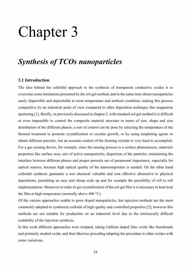
53
Chapter 3
Synthesis of TCOs nanoparticles
3.1 Introduction
The idea behind the colloidal approach to the synthesis of transparent conductive oxides is to
overcome some limitations presented by the sol-gel method, and in the same time obtain nanoparticles
easily dispersible and depositable at room temperature and ambient condition, making this process
competitive by an industrial point of view compared to other deposition technique like magnetron
sputtering [1]. Briefly, as previously discussed in chapter 2, with standard sol-gel method it is difficult
or even impossible to control the composite material structure in terms of size, shape and size
distribution of the different phases; a sort of control can be done by selecting the temperature of the
thermal treatment to promote crystallization or crystals growth, or by using templating agents to
obtain different porosity, but an accurate control of the forming crystals is very hard to accomplish.
For a gas sensing device, for example, since the sensing process is a surface phenomenon, materials
properties like surface area, size of active nanoparticles, dispersion of the particles, maintaining the
interface between different phases and proper porosity are of paramount importance, especially for
optical sensors, because high optical quality of the nanocomposites is needed. On the other hand
colloidal synthesis guarantee a wet chemical valuable and cost effective alternative to physical
depositions, permitting an easy and cheap scale up and for example the possibility of roll to roll
implementation. Moreover in order to get crystallization of the sol-gel film it is necessary to heat treat
the film at high temperature (normally above 400 °C).
Of the various approaches usable to grow doped nanoparticles, hot injection methods are the most
commonly adopted to synthesize colloids of high quality and controlled properties [2]; however this
methods are not suitable for production on an industrial level due to the intrinsically difficult
scalability of the injection synthesis.
In this work different approaches were tempted, taking Gallium doped Zinc oxide like benchmark
and primarily studied oxide, and then likewise preceding adapting the procedure to other oxides with
some variations.
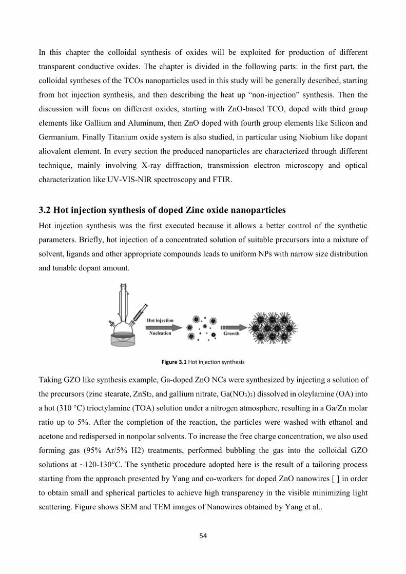
54
In this chapter the colloidal synthesis of oxides will be exploited for production of different
transparent conductive oxides. The chapter is divided in the following parts: in the first part, the
colloidal syntheses of the TCOs nanoparticles used in this study will be generally described, starting
from hot injection synthesis, and then describing the heat up “non-injection” synthesis. Then the
discussion will focus on different oxides, starting with ZnO-based TCO, doped with third group
elements like Gallium and Aluminum, then ZnO doped with fourth group elements like Silicon and
Germanium. Finally Titanium oxide system is also studied, in particular using Niobium like dopant
aliovalent element. In every section the produced nanoparticles are characterized through different
technique, mainly involving X-ray diffraction, transmission electron microscopy and optical
characterization like UV-VIS-NIR spectroscopy and FTIR.
3.2 Hot injection synthesis of doped Zinc oxide nanoparticles
Hot injection synthesis was the first executed because it allows a better control of the synthetic
parameters. Briefly, hot injection of a concentrated solution of suitable precursors into a mixture of
solvent, ligands and other appropriate compounds leads to uniform NPs with narrow size distribution
and tunable dopant amount.
Figure 3.1 Hot injection synthesis
Taking GZO like synthesis example, Ga-doped ZnO NCs were synthesized by injecting a solution of
the precursors (zinc stearate, ZnSt2, and gallium nitrate, Ga(NO3)3) dissolved in oleylamine (OA) into
a hot (310 °C) trioctylamine (TOA) solution under a nitrogen atmosphere, resulting in a Ga/Zn molar
ratio up to 5%. After the completion of the reaction, the particles were washed with ethanol and
acetone and redispersed in nonpolar solvents. To increase the free charge concentration, we also used
forming gas (95% Ar/5% H2) treatments, performed bubbling the gas into the colloidal GZO
solutions at ~120-130°C. The synthetic procedure adopted here is the result of a tailoring process
starting from the approach presented by Yang and co-workers for doped ZnO nanowires [ ] in order
to obtain small and spherical particles to achieve high transparency in the visible minimizing light
scattering. Figure shows SEM and TEM images of Nanowires obtained by Yang et al..

55
Figure 3.2 SEM and TEM images of ZnO nanowires synthesized by decomposing zinc acetate at ∼300 °C in trioctylamine. [3]
The main purpose in this part of the work is controlling materials production both from morphological
and compositional point of view. Indeed particular shapes and sizes are prerequisites for some
applications, so a precise control on the particles growth is mandatory; moreover controlling the
composition (e.g. dopant concentration) is the main way to modify optical and electrical properties
of the oxide.
Figure 3.3 Some characterization of GZO NPs obtained via hot injection method [4] a) XRD pattern of doped ZnO, and ZnO database
position peaks for comparison and NPs UV-VIS-NIR absorption b,c) TEM images of undoped and doped ZnO NPs
This synthesis was optimized by our group [4]. It leads to NPs with typical ZnO wurtzite structure,
like shown in figure 3.3, and to elongated nanoparticles but with an aspect ratio more close to 1
56
compared to the nanowires obtained by Yang. The effect of dopant ions in the structural properties of
ZnO colloids has been investigated recently, confirming their active role in defining the size and
shape of the synthesized NCs. Performing a synthesis of undoped ZnO NCs, using a mixture of 97%
ZnSt2 and 3% zinc nitrate, Zn(NO3)2 there was no appreciable difference in size and shape in
comparison with the ZnO NCs synthesized starting from pure ZnSt2, suggesting a role of Ga3+ rather
than NO3 in affecting the shape of ZnO colloids. The Ga(NO3)3 effect in promoting the elongated
shape of ZnO NCs has been observed also in the past, where more uniform GZO nanowires could be
obtained with respect to AZO and undoped ZnO ones [5].
Doping efficiency can be indirectly evaluated and compared by near infrared absorption that is linked
to carrier concentration in the crystal [6]. In particular, with carrier density increasing, the LSPR in
the infrared increases in frequencies, blue-shifting.
One problem of this approach is that increasing nominal dopant reagents amount, no ulterior
increment or shifting in the plasmonic resonance due to the carrier concentration increment after 5%
dopant nominal is observed [4].
On the other hand hot injection synthesis, as discussed in chapter 2, is quite hardly scalable and not
indicated for industrial applications.
In this work almost all efforts therefore were focused to obtain the same performance of TCOs NPs
obtained from hot injection from TCOs NPs obtained via heat-up non-injection synthesis. NPs
obtained via injection synthesis were used like benchmark, to compare the performance of the new
route, both from the point of view of nanoparticles properties and of the functionality of the produced
thin films.
3.3 Heat up synthesis of doped Zinc oxide nanoparticles
Heat up synthesis was then the route chosen to obtain the NPs of transparent conductor oxides,
keeping always in mind the possible future industrial applications. Regarding the heat-up synthesis
of doped zinc oxide, it builds on work of Peng et al.[7], who showed that under aliphatic condition,
esterification of zinc carboxylates with alcohol results in the formation of hydroxylated species,
which condense to nucleate ZnO nanoparticles. In that work Zinc stearate was found to be stable in
hydrocarbon solvents with the reaction temperature up to 320 °C. The FTIR spectrum, visible in
figure 3.4, before the addition of the alcohol was dominated by the -CH2- vibration (the strongest
band at 1466 cm-1 in all FTIR spectra) and -COO- asymmetric vibration (1536 cm-1) in the 1000-2000
cm-1 spectrum window. However, with alcohol added in, zinc stearate immediately became unstable
and it decomposed quite rapidly. For instance, a few minutes after the addition of the alcohol, the -

57
COO- asymmetric vibration peak decreased by about 95% (relative to the -CH2- vibration band), and
an ester –C=O vibration band (1730 cm-1) appeared.
Figure 3.4 Left: Size and shape evolution of ZnO nanocrystals demonstrated by TEM images. Right: FTIR spectra of the reaction
mixture taken at different stages [7].
The initial nanocrystals formed by this reaction were faceted wurtzite nanocrystals with a relatively
broad size and shape distribution (Figure 3.4, image A) and they are stable to further heating. A
reasonable hypothesis for the unusual stability of the resulting nanocrystals discussed in the above
paragraph is as follows. After all precursors were consumed, growth of the nanocrystals could only
occur through Ostwald ripening. Ostwald ripening basically occurs by dissolving the monomers from
relatively small nanocrystals into solution and growing them back onto relatively large ones among
the distribution. However, there were no free ligands in the solution for stabilizing the monomers in
this case, indicated by the FTIR spectrum. The ultimate instability of the monomers, because of a
lack of ligands, should thus make Ostwald ripening impossible. This hypothesis was tested by
introducing some free ligands, fatty acids, into the reaction system. Although the nanocrystals as well
as the entire reaction system were stable for hours under the above conditions, some dramatic changes
were observed when stearic acid was introduced into the reaction system. The nanocrystals were
eventually converted to stable pyramid-shaped ones, nanopyramids, which appeared triangular in
TEM images (images B and D in Figure 3.4). The stable nanopyramids became unstable again if
additional fatty acids were added into the reaction solution. Careful examination of the temporal
evolution of the particle morphology revealed that the addition of fatty acids into the reaction solution
of the nanopyramids converted the nanopyramids (image B, Figure 3.4) into relatively small dot-
shaped ones (image C, Figure 3.4), and then, these dot-shaped nanocrystals grew back to stable
nanopyramids (image D, Figure 3.4). This nanopyramid-nanodot-nanopyramid transition could be

58
repeated for several cycles if the total number of moles of stearate from the initial zinc stearate and
the stearic acid added afterward was not more than the alcohol originally injected in. Then it’s
necessary to take into account that nanoparticles change morphology after nucleation, and use a
particular ratio between reagents (alcohol and fatty acid for example) to stop the growth at the desired
morphology.
In the next sections main results in term of heat up TCOs synthesis are presented.
3.4 GZO Synthesis and nanocrystals characterization
3.4.1 Gallium doped zinc oxide synthesis
Gallium doped Zinc oxide NPs were synthetized through a non-aqueous heat up colloidal method.
Briefly, in a typical synthesis of ZnO NPs, 1.26 g Zn stearate (Zn St), 3.2 g 1-dodecanol (1-DDol)
and 1.76 g Oleic acid (OA) were mixed together in a round bottom flask, using 21 ml 1-Octadecene
(ODE) as non-coordinating solvent. To obtain doped NPs, a certain amount of Gallium
acetylacetonate (Ga acac) was added (36 mg and 73 mg to obtain, for example, nominal doping levels
of 5% mol and 10% mol for Ga). Then the round bottom flask was connected to a shlenk line,
degassed and maintained in inert atmosphere for the duration of whole synthesis. Solution was then
heated to 130-140°C, becoming transparent, and maintained at that temperature for 45 min; lastly it
was heated to the final temperature of 240°C under strong stirring and at slow heating rate. Solution
was maintained at 240°C for 3h, to ensure dopant incorporation and particles homogeneous growing,
and then cooled down to room temperature.
Figure 3.5 Reaction between the zinc precursor or the dopant precursor and an alcohol leading to the formation of esters and
hydroxylated metal species which eventually condense to form doped ZnO NCs
The reaction mechanism used mainly in this work is presented in figure 3.5: it relies on the irreversible
esterification between the carboxylate groups, which complex the metals and the hydroxyl moieties
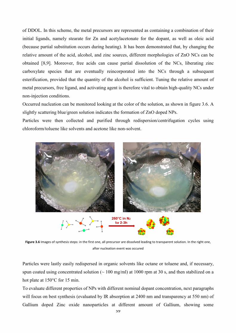
59
of DDOL. In this scheme, the metal precursors are represented as containing a combination of their
initial ligands, namely stearate for Zn and acetylacetonate for the dopant, as well as oleic acid
(because partial substitution occurs during heating). It has been demonstrated that, by changing the
relative amount of the acid, alcohol, and zinc sources, different morphologies of ZnO NCs can be
obtained [8,9]. Moreover, free acids can cause partial dissolution of the NCs, liberating zinc
carboxylate species that are eventually reincorporated into the NCs through a subsequent
esterification, provided that the quantity of the alcohol is sufficient. Tuning the relative amount of
metal precursors, free ligand, and activating agent is therefore vital to obtain high-quality NCs under
non-injection conditions.
Occurred nucleation can be monitored looking at the color of the solution, as shown in figure 3.6. A
slightly scattering blue/green solution indicates the formation of ZnO doped NPs.
Particles were then collected and purified through redispersion/centrifugation cycles using
chloroform/toluene like solvents and acetone like non-solvent.
Figure 3.6 Images of synthesis steps: in the first one, all precursor are dissolved leading to transparent solution. In the right one,
after nucleation event was occured
Particles were lastly easily redispersed in organic solvents like octane or toluene and, if necessary,
spun coated using concentrated solution (~ 100 mg/ml) at 1000 rpm at 30 s, and then stabilized on a
hot plate at 150°C for 15 min.
To evaluate different properties of NPs with different nominal dopant concentration, next paragraphs
will focus on best synthesis (evaluated by IR absorption at 2400 nm and transparency at 550 nm) of
Gallium doped Zinc oxide nanoparticles at different amount of Gallium, showing some

60
characterization, in particular XRD measurement on NPs drop casted on glass substrates, TEM
measurements and optical properties of NPs dispersed in appropriate solvents.
3.4.2 XRD characterization
GZO NPs obtained with this synthesis present the wurtzite crystalline structure, with a typical
crystallite dimension of about 10 nm, depending on synthetic procedure, reagents ratio and dopant
concentration. In particular, increasing Gallium precursor (Gallium acetylacetonate) amount, become
noticeable a slight increase in particles size: it is known that dopant ions play an active role in defining
shape and dimension in colloidal nanocrystals. This effect will be evaluated also through TEM
images, presented later. XRD patterns of GZO NPs deposited by drop casting are shown in figure
3.7, compared to standard ZnO structure (JCPDS No. 36-1451). All samples showed clear and sharp
peaks with no particular preferred orientation. Like in other previous works [5,6], no difference in
peaks position and consequently in lattice parameters are appreciable between doped and undoped
zinc oxide, probably for Gallium and Zinc similar ionic radius. Mean crystallite size were calculated
using Sherrer equation from XRD pattern; results are presented in Table 3.1.
20111
2
20010
311
0
102
101
002
20%
0%
5%Inte
nsity (
a.u
.)
10%
100
20 30 40 50 60 70
2 (°)
Figure 3.7 XRD patterns for GZO NPs deposited by drop casting samples with Ga = 0%, 5%, 10%, 20% mol nominal. Theoretical
diffraction peak positions for ZnO (JCPDS No. 36-1451) are also reported.
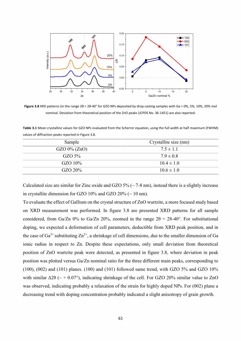
61
28 30 32 34 36 38 40 0 5 10 15 20
-0,05
0,00
0,05
0,10
0,15
0,20
101
002
20%
0%
5%
Inte
nsity (
a.u
.)
2
10%
100
2
Ga/Zn nominal %
100
002
101
Figure 3.8 XRD patterns (in the range 2θ = 28-40° for GZO NPs deposited by drop casting samples with Ga = 0%, 5%, 10%, 20% mol
nominal. Deviation from theoretical position of the ZnO peaks (JCPDS No. 36-1451) are also reported.
Table 3.1 Mean crystalline values for GZO NPs evaluated from the Scherrer equation, using the full width at half maximum (FWHM)
values of diffraction peaks reported in Figure 3.8.
Sample Crystallite size (nm)
GZO 0% (ZnO) 7.5 ± 1.1
GZO 5% 7.9 ± 0.8
GZO 10% 10.4 ± 1.0
GZO 20% 10.6 ± 1.0
Calculated size are similar for Zinc oxide and GZO 5% (~ 7-8 nm), instead there is a slightly increase
in crystallite dimension for GZO 10% and GZO 20% (~ 10 nm).
To evaluate the effect of Gallium on the crystal structure of ZnO wurtzite, a more focused study based
on XRD measurement was performed. In figure 3.8 are presented XRD patterns for all sample
considered, from Ga/Zn 0% to Ga/Zn 20%, zoomed in the range 2θ = 28-40°. For substitutional
doping, we expected a deformation of cell parameters, deductible from XRD peak position, and in
the case of Ga3+ substituting Zn2+, a shrinkage of cell dimensions, due to the smaller dimension of Ga
ionic radius in respect to Zn. Despite these expectations, only small deviation from theoretical
position of ZnO wurtzite peak were detected, as presented in figure 3.8, where deviation in peak
position was plotted versus Ga/Zn nominal ratio for the three different main peaks, corresponding to
(100), (002) and (101) planes. (100) and (101) followed same trend, with GZO 5% and GZO 10%
with similar Δ2θ (~ + 0.07°), indicating shrinkage of the cell. For GZO 20% similar value to ZnO
was observed, indicating probably a relaxation of the strain for highly doped NPs. For (002) plane a
decreasing trend with doping concentration probably indicated a slight anisotropy of grain growth.
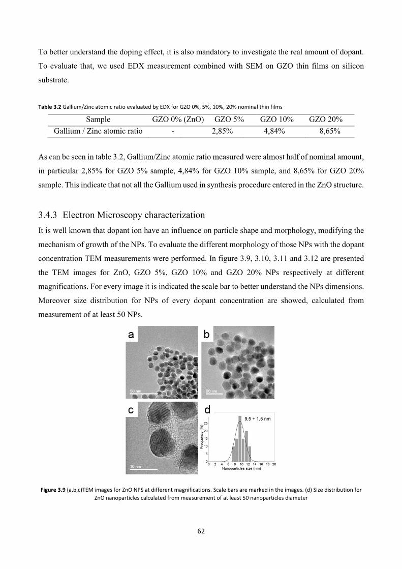
62
To better understand the doping effect, it is also mandatory to investigate the real amount of dopant.
To evaluate that, we used EDX measurement combined with SEM on GZO thin films on silicon
substrate.
Table 3.2 Gallium/Zinc atomic ratio evaluated by EDX for GZO 0%, 5%, 10%, 20% nominal thin films
Sample GZO 0% (ZnO) GZO 5% GZO 10% GZO 20%
Gallium / Zinc atomic ratio - 2,85% 4,84% 8,65%
As can be seen in table 3.2, Gallium/Zinc atomic ratio measured were almost half of nominal amount,
in particular 2,85% for GZO 5% sample, 4,84% for GZO 10% sample, and 8,65% for GZO 20%
sample. This indicate that not all the Gallium used in synthesis procedure entered in the ZnO structure.
3.4.3 Electron Microscopy characterization
It is well known that dopant ion have an influence on particle shape and morphology, modifying the
mechanism of growth of the NPs. To evaluate the different morphology of those NPs with the dopant
concentration TEM measurements were performed. In figure 3.9, 3.10, 3.11 and 3.12 are presented
the TEM images for ZnO, GZO 5%, GZO 10% and GZO 20% NPs respectively at different
magnifications. For every image it is indicated the scale bar to better understand the NPs dimensions.
Moreover size distribution for NPs of every dopant concentration are showed, calculated from
measurement of at least 50 NPs.
Figure 3.9 (a,b,c)TEM images for ZnO NPS at different magnifications. Scale bars are marked in the images. (d) Size distribution for
ZnO nanoparticles calculated from measurement of at least 50 nanoparticles diameter

63
Figure 3.10 (a,b,c) TEM images for GZO 5% NPS at different magnifications. Scale bars are marked in the images. (d) Size
distribution for GZO 5% nanoparticles calculated from measurement of at least 50 nanoparticles diameter
Figure 3.11 (a,b,c) TEM images for GZO 10% NPS at different magnifications. Scale bars are marked in the images. (d) Size
distribution for GZO 10% nanoparticles calculated from measurement of at least 50 nanoparticles diameter
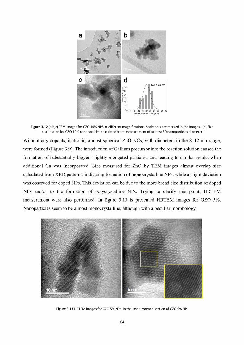
64
Figure 3.12 (a,b,c) TEM images for GZO 10% NPS at different magnifications. Scale bars are marked in the images. (d) Size
distribution for GZO 10% nanoparticles calculated from measurement of at least 50 nanoparticles diameter
Without any dopants, isotropic, almost spherical ZnO NCs, with diameters in the 8–12 nm range,
were formed (Figure 3.9). The introduction of Gallium precursor into the reaction solution caused the
formation of substantially bigger, slightly elongated particles, and leading to similar results when
additional Ga was incorporated. Size measured for ZnO by TEM images almost overlap size
calculated from XRD patterns, indicating formation of monocrystalline NPs, while a slight deviation
was observed for doped NPs. This deviation can be due to the more broad size distribution of doped
NPs and/or to the formation of polycrystalline NPs. Trying to clarify this point, HRTEM
measurement were also performed. In figure 3.13 is presented HRTEM images for GZO 5%.
Nanoparticles seem to be almost monocrystalline, although with a peculiar morphology.
Figure 3.13 HRTEM images for GZO 5% NPs. In the inset, zoomed section of GZO 5% NP.
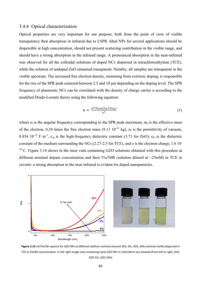
65
3.4.4 Optical characterization
Optical properties are very important for our purpose, both from the point of view of visible
transparency then absorption in infrared due to LSPR. Ideal NPs for several applications should be
dispersible at high concentration, should not present scattering contribution in the visible range, and
should have a strong absorption in the infrared range. A pronounced absorption in the near-infrared
was observed for all the colloidal solutions of doped NCs dispersed in tetrachloroethylene (TCE),
while the solution of undoped ZnO remained transparent. Notably, all samples are transparent in the
visible spectrum. The increased free electron density, stemming from extrinsic doping, is responsible
for the rise of the SPR peak centered between 2.5 and 10 μm depending on the doping level. The SPR
frequency of plasmonic NCs can be correlated with the density of charge carrier n according to the
modified Drude-Lorentz theory using the following equation:
𝑛 = 𝜔2𝑚𝑒𝜀0(𝜀∞+2𝜀𝑚)
𝑒2 (1)
where ω is the angular frequency corresponding to the SPR peak maximum, me is the effective mass
of the electron, 0.24 times the free electron mass (9.11 10-31 kg), ε0 is the permittivity of vacuum,
8.854 10-12 F m-1, 𝜀∞ is the high-frequency dielectric constant (3.71 for ZnO), εm is the dielectric
constant of the medium surrounding the NCs (2.27-2.5 for TCE), and e is the electron charge, 1.6 10-
19 C. Figure 3.14 shows in the inset vials containing GZO solutions obtained with this procedure at
different nominal dopant concentration and their Vis/NIR (solution diluted at ~25mM) in TCE in
cuvette: a strong absorption in the near infrared is evident for doped nanoparticles.
500 1000 1500 2000 2500
0
1
2
0%
5%
10%
Abs
Wavelength (nm)
20%
% Ga nom
Figure 3.14 UV/Vis/Nir spectra for GZO NPs at different Gallium nominal amount (0%, 5%, 10%, 20% nominal mol%) dispersed in
TCE at 25mM concentration. In the right image vials containing same GZO NPs in chloroform are showed (from left to right, ZnO,
GZO 5%, GZO 10%)
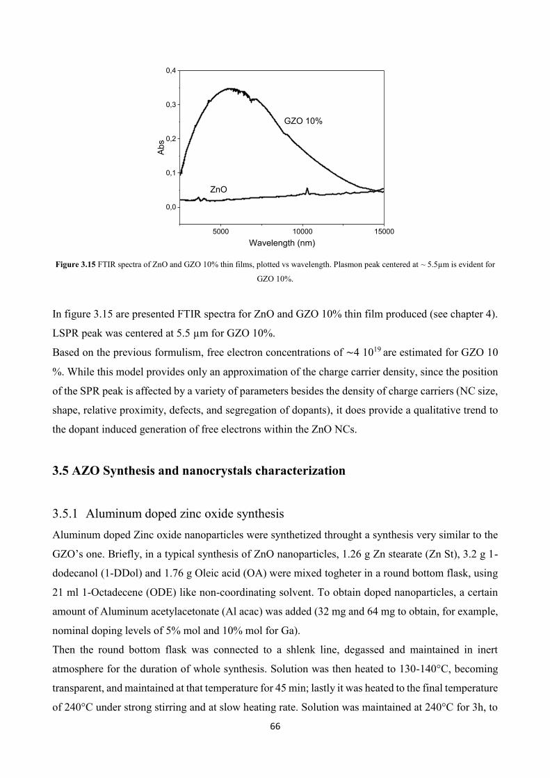
66
5000 10000 15000
0,0
0,1
0,2
0,3
0,4
GZO 10%
Abs
Wavelength (nm)
ZnO
Figure 3.15 FTIR spectra of ZnO and GZO 10% thin films, plotted vs wavelength. Plasmon peak centered at ~ 5.5µm is evident for
GZO 10%.
In figure 3.15 are presented FTIR spectra for ZnO and GZO 10% thin film produced (see chapter 4).
LSPR peak was centered at 5.5 µm for GZO 10%.
Based on the previous formulism, free electron concentrations of ∼4 1019 are estimated for GZO 10
%. While this model provides only an approximation of the charge carrier density, since the position
of the SPR peak is affected by a variety of parameters besides the density of charge carriers (NC size,
shape, relative proximity, defects, and segregation of dopants), it does provide a qualitative trend to
the dopant induced generation of free electrons within the ZnO NCs.
3.5 AZO Synthesis and nanocrystals characterization
3.5.1 Aluminum doped zinc oxide synthesis
Aluminum doped Zinc oxide nanoparticles were synthetized throught a synthesis very similar to the
GZO’s one. Briefly, in a typical synthesis of ZnO nanoparticles, 1.26 g Zn stearate (Zn St), 3.2 g 1-
dodecanol (1-DDol) and 1.76 g Oleic acid (OA) were mixed togheter in a round bottom flask, using
21 ml 1-Octadecene (ODE) like non-coordinating solvent. To obtain doped nanoparticles, a certain
amount of Aluminum acetylacetonate (Al acac) was added (32 mg and 64 mg to obtain, for example,
nominal doping levels of 5% mol and 10% mol for Ga).
Then the round bottom flask was connected to a shlenk line, degassed and maintained in inert
atmosphere for the duration of whole synthesis. Solution was then heated to 130-140°C, becoming
transparent, and maintained at that temperature for 45 min; lastly it was heated to the final temperature
of 240°C under strong stirring and at slow heating rate. Solution was maintained at 240°C for 3h, to
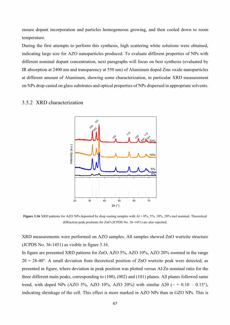
67
ensure dopant incorporation and particles homogeneous growing, and then cooled down to room
temperature.
During the first attempts to perform this synthesis, high scattering white solutions were obtained,
indicating large size for AZO nanoparticles produced. To evaluate different properties of NPs with
different nominal dopant concentration, next paragraphs will focus on best synthesis (evaluated by
IR absorption at 2400 nm and transparency at 550 nm) of Aluminum doped Zinc oxide nanoparticles
at different amount of Aluminum, showing some characterization, in particular XRD measurement
on NPs drop casted on glass substrates and optical properties of NPs dispersed in appropriate solvents.
3.5.2 XRD characterization
20111
2
20010
311
0
102
101
002
20%
0%
5%
Inte
nsity (
a.u
.)
10%
100
20 30 40 50 60 70
2 (°)
Figure 3.16 XRD patterns for AZO NPs deposited by drop casting samples with Al = 0%, 5%, 10%, 20% mol nominal. Theoretical
diffraction peak positions for ZnO (JCPDS No. 36-1451) are also reported.
XRD measurements were performed on AZO samples. All samples showed ZnO wurtzite structure
(JCPDS No. 36-1451) as visible in figure 3.16.
In figure are presented XRD patterns for ZnO, AZO 5%, AZO 10%, AZO 20% zoomed in the range
2θ = 28-40°. A small deviation from theoretical position of ZnO wurtzite peak were detected, as
presented in figure, where deviation in peak position was plotted versus Al/Zn nominal ratio for the
three different main peaks, corresponding to (100), (002) and (101) planes. All planes followed same
trend, with doped NPs (AZO 5%, AZO 10%, AZO 20%) with similar Δ2θ (~ + 0.10 – 0.15°),
indicating shrinkage of the cell. This effect is more marked in AZO NPs than in GZO NPs. This is

68
consistent with the fact that Al ionic radius is smaller than Ga ionic radius, 67 pm for Al3+ and 75 pm
for Ga3+, versus 88 pm for Zn, creating a shrinkage effect on cell parameters.
28 30 32 34 36 38 40 0 5 10 15 20
-0,05
0,00
0,05
0,10
0,15
0,20
101
002
20%
0%
5%
Inte
nsity (
a.u
.)
2 (°)
10%
100
Al/Zn nominal %
100
002
101
Figure 3.17 XRD patterns (in the range 2θ = 28-40° for AZO NPs deposited by drop casting samples with Al = 0%, 5%, 10%, 20% mol
nominal. Deviation from theoretical position of the ZnO peaks (JCPDS No. 36-1451) are also reported.
Table 3.3 Mean crystallite diameter s for AZO NPs evaluated from the Scherrer equation, using the full width at half maximum
(FWHM) of diffraction peaks reported in Figure 3.17.
Sample Crystallite size (nm)
AZO 0% (ZnO) 7.5 ± 1.1
AZO 5% 9.7 ± 0.3
AZO 10% 14.3 ± 0.3
AZO 20% 16.6 ± 0.8
Crystallite mean diameter was evaluated by Sherrer equation. Dopant element addition lead to a slight
increasing in crystallite size, as presented in table 3.3. With respect to GZO crystallite size, they were
also slightly bigger (9-16 nm for AZO versus 8-10 nm for GZO). SEM images in chapter 4 for AZO
thin films showed even bigger particles, suggesting polycrystalline formation.
EDX measurement performed on AZO films, showed in table 3.4, indicate a very low content of
Aluminum in AZO 5%, while a very high amount for AZ0 20% (14.28%)
Table 3.4. Aluminum/Zinc atomic ratio evaluated by EDX for AZO 0%, 5%, 10%, 20% nominal thin films
Sample AZO 0% (ZnO) AZO 5% AZO 10% AZO 20%
Aluminum / Zinc atomic
ratio
- 1.3% 5.31% 14.28%
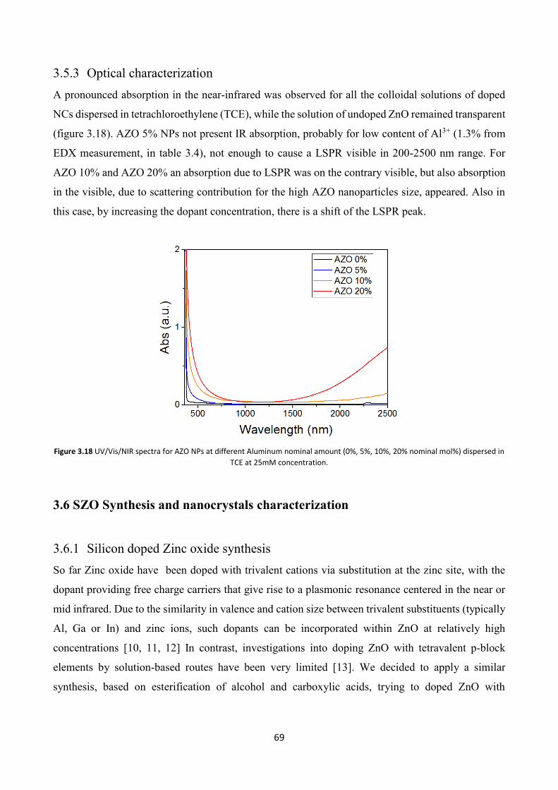
69
3.5.3 Optical characterization
A pronounced absorption in the near-infrared was observed for all the colloidal solutions of doped
NCs dispersed in tetrachloroethylene (TCE), while the solution of undoped ZnO remained transparent
(figure 3.18). AZO 5% NPs not present IR absorption, probably for low content of Al3+ (1.3% from
EDX measurement, in table 3.4), not enough to cause a LSPR visible in 200-2500 nm range. For
AZO 10% and AZO 20% an absorption due to LSPR was on the contrary visible, but also absorption
in the visible, due to scattering contribution for the high AZO nanoparticles size, appeared. Also in
this case, by increasing the dopant concentration, there is a shift of the LSPR peak.
Figure 3.18 UV/Vis/NIR spectra for AZO NPs at different Aluminum nominal amount (0%, 5%, 10%, 20% nominal mol%) dispersed in
TCE at 25mM concentration.
3.6 SZO Synthesis and nanocrystals characterization
3.6.1 Silicon doped Zinc oxide synthesis
So far Zinc oxide have been doped with trivalent cations via substitution at the zinc site, with the
dopant providing free charge carriers that give rise to a plasmonic resonance centered in the near or
mid infrared. Due to the similarity in valence and cation size between trivalent substituents (typically
Al, Ga or In) and zinc ions, such dopants can be incorporated within ZnO at relatively high
concentrations [10, 11, 12] In contrast, investigations into doping ZnO with tetravalent p-block
elements by solution-based routes have been very limited [13]. We decided to apply a similar
synthesis, based on esterification of alcohol and carboxylic acids, trying to doped ZnO with
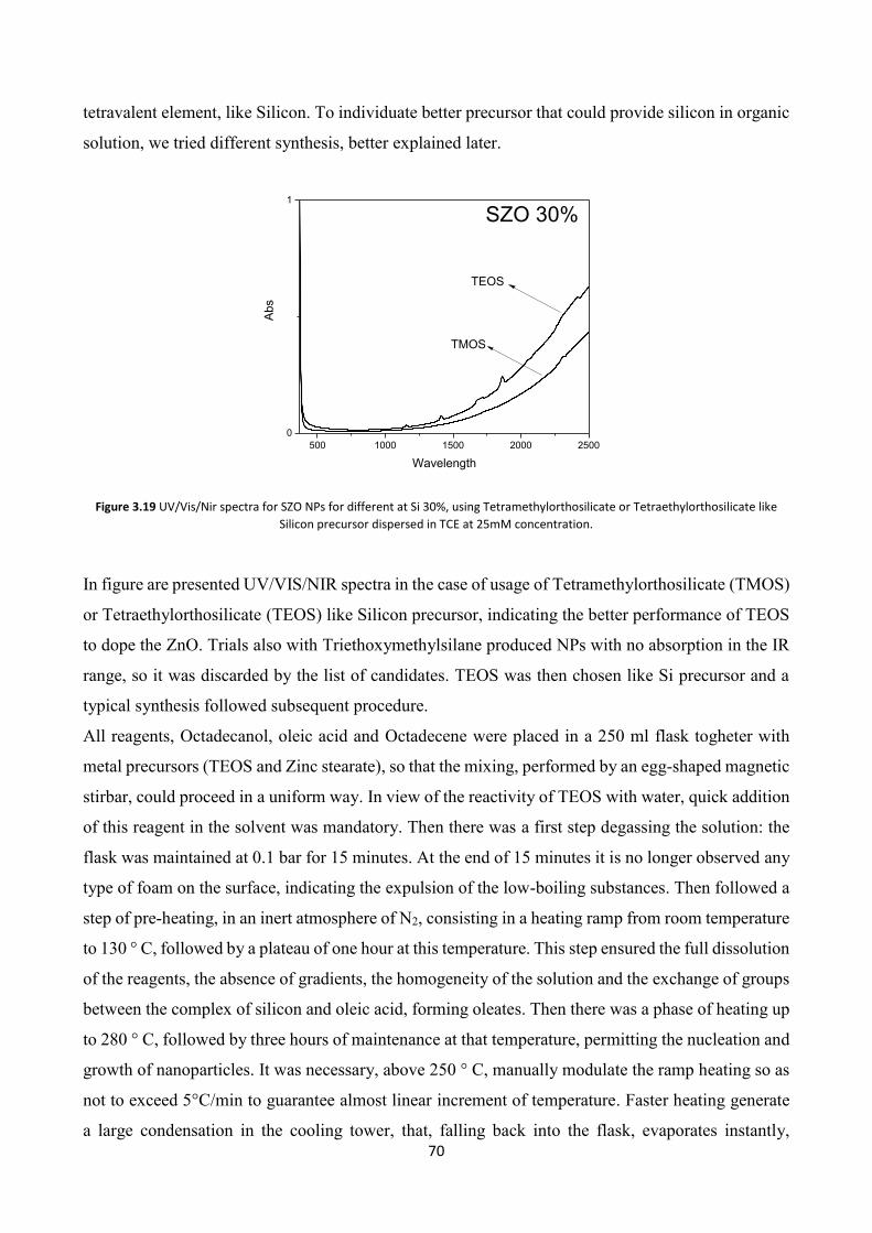
70
tetravalent element, like Silicon. To individuate better precursor that could provide silicon in organic
solution, we tried different synthesis, better explained later.
Figure 3.19 UV/Vis/Nir spectra for SZO NPs for different at Si 30%, using Tetramethylorthosilicate or Tetraethylorthosilicate like
Silicon precursor dispersed in TCE at 25mM concentration.
In figure are presented UV/VIS/NIR spectra in the case of usage of Tetramethylorthosilicate (TMOS)
or Tetraethylorthosilicate (TEOS) like Silicon precursor, indicating the better performance of TEOS
to dope the ZnO. Trials also with Triethoxymethylsilane produced NPs with no absorption in the IR
range, so it was discarded by the list of candidates. TEOS was then chosen like Si precursor and a
typical synthesis followed subsequent procedure.
All reagents, Octadecanol, oleic acid and Octadecene were placed in a 250 ml flask togheter with
metal precursors (TEOS and Zinc stearate), so that the mixing, performed by an egg-shaped magnetic
stirbar, could proceed in a uniform way. In view of the reactivity of TEOS with water, quick addition
of this reagent in the solvent was mandatory. Then there was a first step degassing the solution: the
flask was maintained at 0.1 bar for 15 minutes. At the end of 15 minutes it is no longer observed any
type of foam on the surface, indicating the expulsion of the low-boiling substances. Then followed a
step of pre-heating, in an inert atmosphere of N2, consisting in a heating ramp from room temperature
to 130 ° C, followed by a plateau of one hour at this temperature. This step ensured the full dissolution
of the reagents, the absence of gradients, the homogeneity of the solution and the exchange of groups
between the complex of silicon and oleic acid, forming oleates. Then there was a phase of heating up
to 280 ° C, followed by three hours of maintenance at that temperature, permitting the nucleation and
growth of nanoparticles. It was necessary, above 250 ° C, manually modulate the ramp heating so as
not to exceed 5°C/min to guarantee almost linear increment of temperature. Faster heating generate
a large condensation in the cooling tower, that, falling back into the flask, evaporates instantly,
500 1000 1500 2000 2500
0
1
TMOS
Abs
Wavelength
SZO 30%
TEOS

71
violently disrupting the dynamic equilibrium and stirring of the synthesis and making it difficult to
achieve the plateau at 280 °C. At the end of the reaction the cooling was performed also in an inert
atmosphere. The yield nominal rated is 75%, calculated on a weight basis. Then it was adopted a
cleaning protocol consisting of consecutive cycles of NPs washing. Firstly raw solution was
centrifuged, depositing the NPs by flocculation adding non-solvent like acetone. It was
experimentally verified that precipitates almost exclusive of the nanoparticles using an amount of
acetone twice that of the solvent (about 80 ml) and placing the mixture in a centrifuge at 4000 rpm
for 5 minutes.
The SZO NPs were dispersed in non-polar solvents, producing clear solutions and yellow-green. The
use of toluene, maintaining the uniformity in time and not generating precipitates, it allows the long-
term storage.
To evaluate the capability to scale up of this synthesis, some attempts with double amount of reagents
(2x) were performed. In figure 3.20 are showed the spectra for typical synthesis and 2x synthesis,
proving the scalability of the reaction. However 2x synthesis lead to minor doping yield and
moreover, at Si 30% NPs by 2x synthesis are bigger and their scattering in the visible range cause
loss in transparency.
Figure 3.20 Comparison between UV/Vis/Nir spectra for SZO NPs (10%, 20%, 30%) obtained with standard synthesis and 2x
synthesis dispersed in TCE at 25mM concentration.
500 1000 1500 2000 2500
0
1
500 1000 1500 2000 2500
0
1
1x
1x
1x
2x
2x
30%
20%
Abs
Wavelength (nm)
10%
2x
500 1000 1500 2000 2500
Wavelength (nm)
Wavelength (nm)
Abs
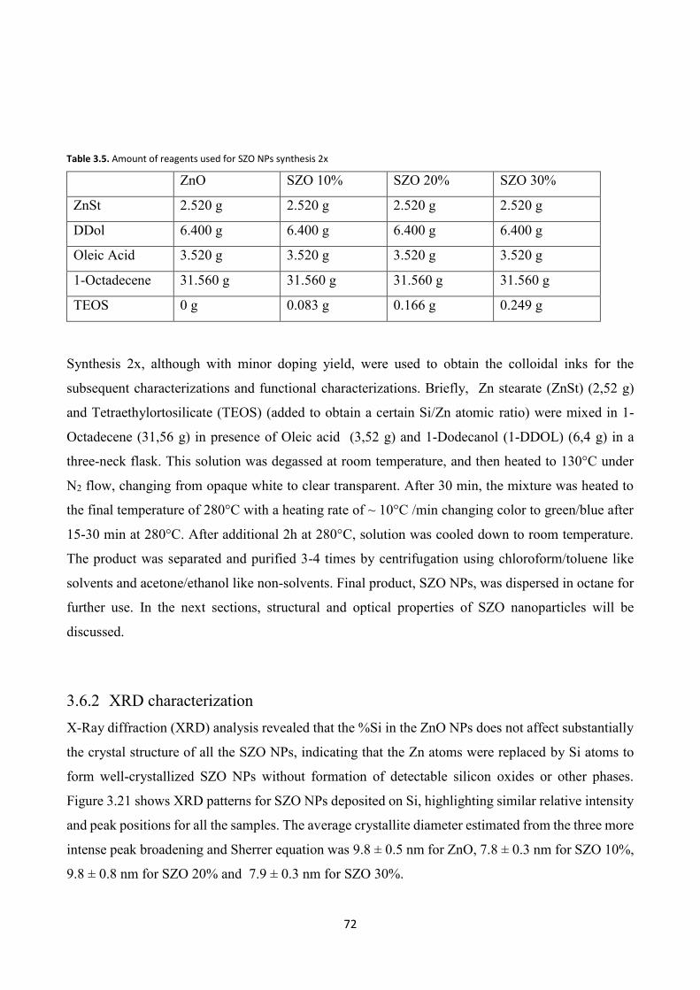
72
Table 3.5. Amount of reagents used for SZO NPs synthesis 2x
ZnO SZO 10% SZO 20% SZO 30%
ZnSt 2.520 g 2.520 g 2.520 g 2.520 g
DDol 6.400 g 6.400 g 6.400 g 6.400 g
Oleic Acid 3.520 g 3.520 g 3.520 g 3.520 g
1-Octadecene 31.560 g 31.560 g 31.560 g 31.560 g
TEOS 0 g 0.083 g 0.166 g 0.249 g
Synthesis 2x, although with minor doping yield, were used to obtain the colloidal inks for the
subsequent characterizations and functional characterizations. Briefly, Zn stearate (ZnSt) (2,52 g)
and Tetraethylortosilicate (TEOS) (added to obtain a certain Si/Zn atomic ratio) were mixed in 1-
Octadecene (31,56 g) in presence of Oleic acid (3,52 g) and 1-Dodecanol (1-DDOL) (6,4 g) in a
three-neck flask. This solution was degassed at room temperature, and then heated to 130°C under
N2 flow, changing from opaque white to clear transparent. After 30 min, the mixture was heated to
the final temperature of 280°C with a heating rate of ~ 10°C /min changing color to green/blue after
15-30 min at 280°C. After additional 2h at 280°C, solution was cooled down to room temperature.
The product was separated and purified 3-4 times by centrifugation using chloroform/toluene like
solvents and acetone/ethanol like non-solvents. Final product, SZO NPs, was dispersed in octane for
further use. In the next sections, structural and optical properties of SZO nanoparticles will be
discussed.
3.6.2 XRD characterization
X-Ray diffraction (XRD) analysis revealed that the %Si in the ZnO NPs does not affect substantially
the crystal structure of all the SZO NPs, indicating that the Zn atoms were replaced by Si atoms to
form well-crystallized SZO NPs without formation of detectable silicon oxides or other phases.
Figure 3.21 shows XRD patterns for SZO NPs deposited on Si, highlighting similar relative intensity
and peak positions for all the samples. The average crystallite diameter estimated from the three more
intense peak broadening and Sherrer equation was 9.8 ± 0.5 nm for ZnO, 7.8 ± 0.3 nm for SZO 10%,
9.8 ± 0.8 nm for SZO 20% and 7.9 ± 0.3 nm for SZO 30%.
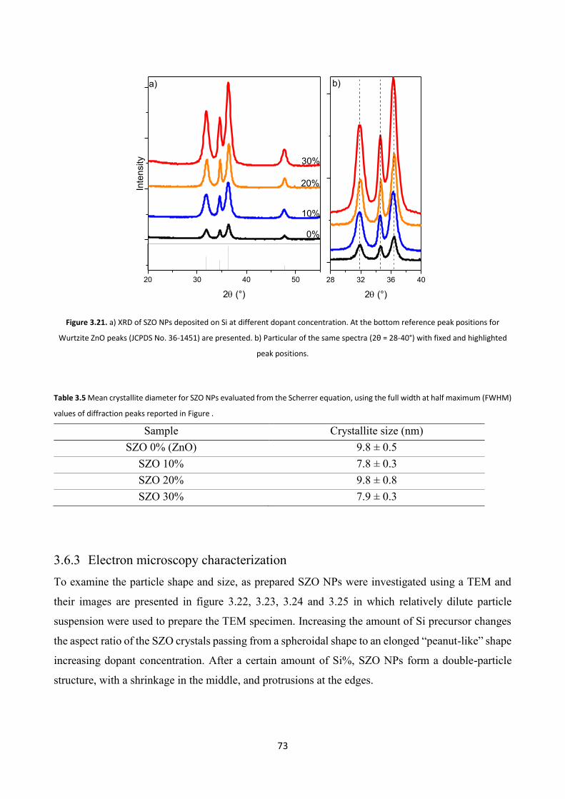
73
20 30 40 50 28 32 36 40
b)
30%
20%
10%
Inte
nsity
2 (°)
0%
a)
2 (°)
Figure 3.21. a) XRD of SZO NPs deposited on Si at different dopant concentration. At the bottom reference peak positions for
Wurtzite ZnO peaks (JCPDS No. 36-1451) are presented. b) Particular of the same spectra (2θ = 28-40°) with fixed and highlighted
peak positions.
Table 3.5 Mean crystallite diameter for SZO NPs evaluated from the Scherrer equation, using the full width at half maximum (FWHM)
values of diffraction peaks reported in Figure .
Sample Crystallite size (nm)
SZO 0% (ZnO) 9.8 ± 0.5
SZO 10% 7.8 ± 0.3
SZO 20% 9.8 ± 0.8
SZO 30% 7.9 ± 0.3
3.6.3 Electron microscopy characterization
To examine the particle shape and size, as prepared SZO NPs were investigated using a TEM and
their images are presented in figure 3.22, 3.23, 3.24 and 3.25 in which relatively dilute particle
suspension were used to prepare the TEM specimen. Increasing the amount of Si precursor changes
the aspect ratio of the SZO crystals passing from a spheroidal shape to an elonged “peanut-like” shape
increasing dopant concentration. After a certain amount of Si%, SZO NPs form a double-particle
structure, with a shrinkage in the middle, and protrusions at the edges.

74
Figure 3.22 (a,b,c) TEM images for ZnO NPS at different magnifications. Scale bars are marked in the images. (d) Size distribution for
ZnO nanoparticles calculated from measurement of at least 50 nanoparticles diameter
Figure 3.23 (a,b,c) TEM images for SZO 10% NPS at different magnifications. Scale bars are marked in the images. (d) Size
distribution for SZO 10% nanoparticles calculated from measurement of at least 50 nanoparticles diameter

75
Figure 3.24 (a,b,c) TEM images for SZO 20% NPS at different magnifications. Scale bars are marked in the images. (d) Size
distribution for SZO 20% nanoparticles calculated from measurement of at least 50 nanoparticles diameter
Figure 3.25 (a,b,c) TEM images for SZO 300% NPS at different magnifications. Scale bars are marked in the images. (d) Size
distribution for SZO 30% nanoparticles calculated from measurement of at least 50 nanoparticles diameter
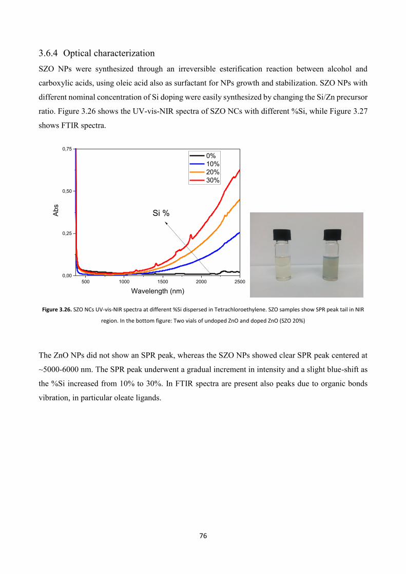
76
3.6.4 Optical characterization
SZO NPs were synthesized through an irreversible esterification reaction between alcohol and
carboxylic acids, using oleic acid also as surfactant for NPs growth and stabilization. SZO NPs with
different nominal concentration of Si doping were easily synthesized by changing the Si/Zn precursor
ratio. Figure 3.26 shows the UV-vis-NIR spectra of SZO NCs with different %Si, while Figure 3.27
shows FTIR spectra.
500 1000 1500 2000 2500
0,00
0,25
0,50
0,75
0%
10%
20%
30%
Abs
Wavelength (nm)
Si %
Figure 3.26. SZO NCs UV-vis-NIR spectra at different %Si dispersed in Tetrachloroethylene. SZO samples show SPR peak tail in NIR
region. In the bottom figure: Two vials of undoped ZnO and doped ZnO (SZO 20%)
The ZnO NPs did not show an SPR peak, whereas the SZO NPs showed clear SPR peak centered at
~5000-6000 nm. The SPR peak underwent a gradual increment in intensity and a slight blue-shift as
the %Si increased from 10% to 30%. In FTIR spectra are present also peaks due to organic bonds
vibration, in particular oleate ligands.
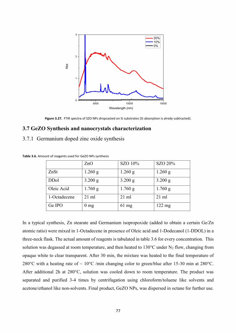
77
5000 10000 15000
0
1
2
3
Abs
Wavelength (nm)
20%
10%
0%
Figure 3.27. FTIR spectra of SZO NPs dropcasted on Si substrates (Si absorption is alredy subtracted).
3.7 GeZO Synthesis and nanocrystals characterization
3.7.1 Germanium doped zinc oxide synthesis
Table 3.6. Amount of reagents used for GeZO NPs synthesis
ZnO SZO 10% SZO 20%
ZnSt 1.260 g 1.260 g 1.260 g
DDol 3.200 g 3.200 g 3.200 g
Oleic Acid 1.760 g 1.760 g 1.760 g
1-Octadecene 21 ml 21 ml 21 ml
Ge IPO 0 mg 61 mg 122 mg
In a typical synthesis, Zn stearate and Germanium isopropoxide (added to obtain a certain Ge/Zn
atomic ratio) were mixed in 1-Octadecene in presence of Oleic acid and 1-Dodecanol (1-DDOL) in a
three-neck flask. The actual amount of reagents is tabulated in table 3.6 for every concentration. This
solution was degassed at room temperature, and then heated to 130°C under N2 flow, changing from
opaque white to clear transparent. After 30 min, the mixture was heated to the final temperature of
280°C with a heating rate of ~ 10°C /min changing color to green/blue after 15-30 min at 280°C.
After additional 2h at 280°C, solution was cooled down to room temperature. The product was
separated and purified 3-4 times by centrifugation using chloroform/toluene like solvents and
acetone/ethanol like non-solvents. Final product, GeZO NPs, was dispersed in octane for further use.
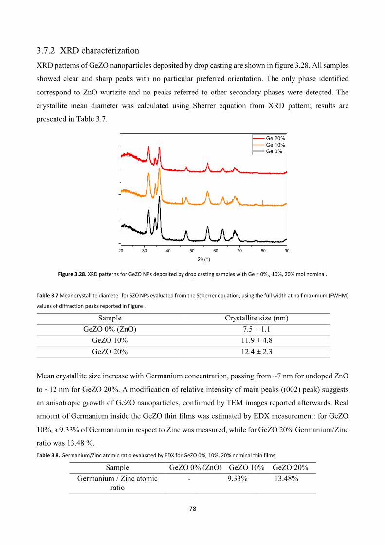
78
3.7.2 XRD characterization
XRD patterns of GeZO nanoparticles deposited by drop casting are shown in figure 3.28. All samples
showed clear and sharp peaks with no particular preferred orientation. The only phase identified
correspond to ZnO wurtzite and no peaks referred to other secondary phases were detected. The
crystallite mean diameter was calculated using Sherrer equation from XRD pattern; results are
presented in Table 3.7.
20 30 40 50 60 70 80 90
2
Ge 20%
Ge 10%
Ge 0%
Figure 3.28. XRD patterns for GeZO NPs deposited by drop casting samples with Ge = 0%,, 10%, 20% mol nominal.
Table 3.7 Mean crystallite diameter for SZO NPs evaluated from the Scherrer equation, using the full width at half maximum (FWHM)
values of diffraction peaks reported in Figure .
Sample Crystallite size (nm)
GeZO 0% (ZnO) 7.5 ± 1.1
GeZO 10% 11.9 ± 4.8
GeZO 20% 12.4 ± 2.3
Mean crystallite size increase with Germanium concentration, passing from ~7 nm for undoped ZnO
to ~12 nm for GeZO 20%. A modification of relative intensity of main peaks ((002) peak) suggests
an anisotropic growth of GeZO nanoparticles, confirmed by TEM images reported afterwards. Real
amount of Germanium inside the GeZO thin films was estimated by EDX measurement: for GeZO
10%, a 9.33% of Germanium in respect to Zinc was measured, while for GeZO 20% Germanium/Zinc
ratio was 13.48 %.
Table 3.8. Germanium/Zinc atomic ratio evaluated by EDX for GeZO 0%, 10%, 20% nominal thin films
Sample GeZO 0% (ZnO) GeZO 10% GeZO 20%
Germanium / Zinc atomic
ratio
- 9.33% 13.48%
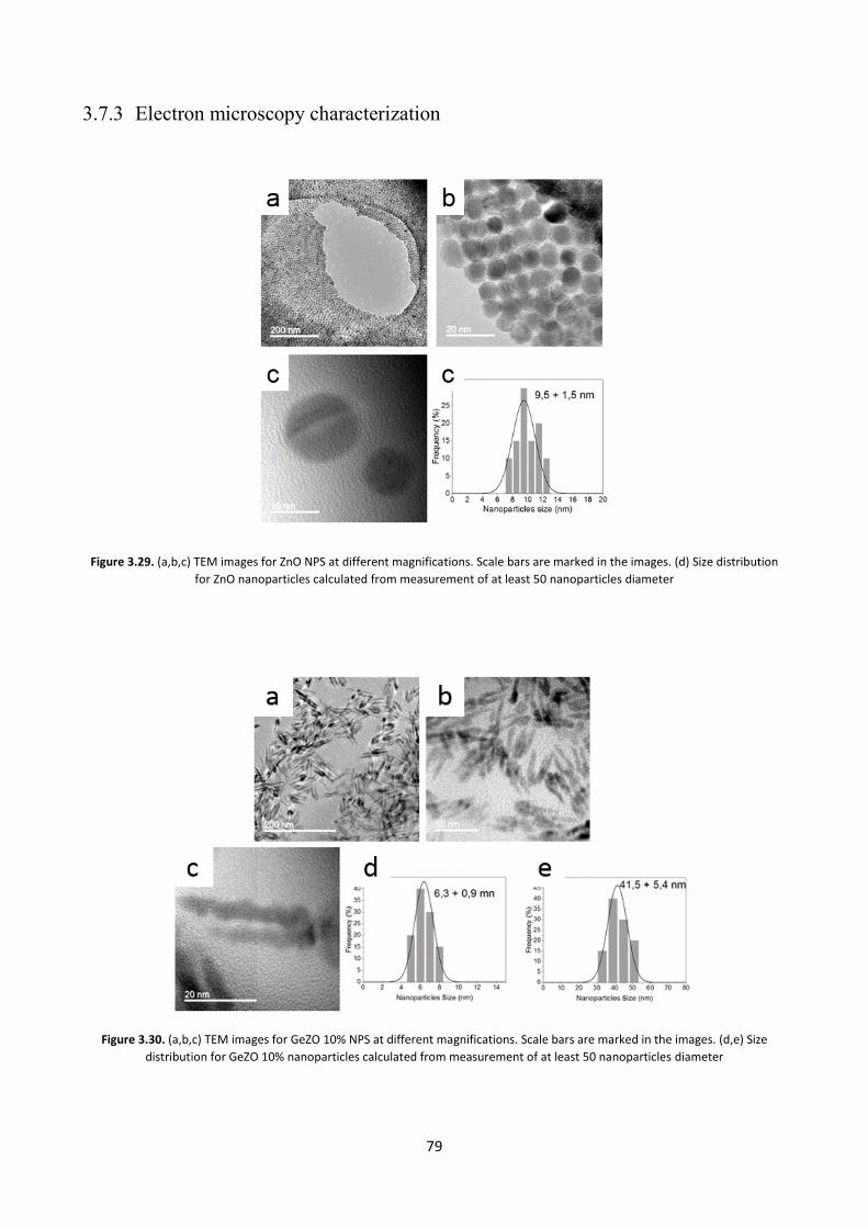
79
3.7.3 Electron microscopy characterization
Figure 3.29. (a,b,c) TEM images for ZnO NPS at different magnifications. Scale bars are marked in the images. (d) Size distribution
for ZnO nanoparticles calculated from measurement of at least 50 nanoparticles diameter
Figure 3.30. (a,b,c) TEM images for GeZO 10% NPS at different magnifications. Scale bars are marked in the images. (d,e) Size
distribution for GeZO 10% nanoparticles calculated from measurement of at least 50 nanoparticles diameter
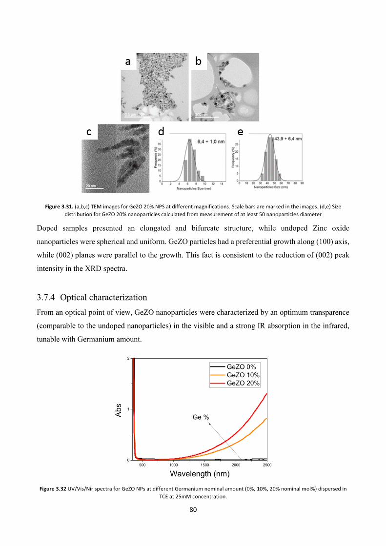
80
Figure 3.31. (a,b,c) TEM images for GeZO 20% NPS at different magnifications. Scale bars are marked in the images. (d,e) Size
distribution for GeZO 20% nanoparticles calculated from measurement of at least 50 nanoparticles diameter
Doped samples presented an elongated and bifurcate structure, while undoped Zinc oxide
nanoparticles were spherical and uniform. GeZO particles had a preferential growth along (100) axis,
while (002) planes were parallel to the growth. This fact is consistent to the reduction of (002) peak
intensity in the XRD spectra.
3.7.4 Optical characterization
From an optical point of view, GeZO nanoparticles were characterized by an optimum transparence
(comparable to the undoped nanoparticles) in the visible and a strong IR absorption in the infrared,
tunable with Germanium amount.
500 1000 1500 2000 2500
0
1
2
Abs
Wavelength (nm)
GeZO 0%
GeZO 10%
GeZO 20%
Ge %
Figure 3.32 UV/Vis/Nir spectra for GeZO NPs at different Germanium nominal amount (0%, 10%, 20% nominal mol%) dispersed in
TCE at 25mM concentration.

81
3.8 NTO Synthesis and nanocrystals characterization
3.8.1 Niobium doped titanium dioxide synthesis
Niobium doped titanium dioxide represent a different system studied. The colloidal synthesis used in
this work refers to the study of Milliron et al. [6], optimized to suit our purposes. This synthesis uses
as precursor of Titanium an organometallic compound (titanium ethoxide or isopropoxide) and
Niobium pentachloride as Niobium precursor. The precursors used in this synthesis are very reactive
in atmospheric environment, due to their affinity to water.
The weighed and the preparation of the synthesis should be carried out in a glove box to avoid the
degradation of the reactants, but this approach would make difficult to produce easy and reproducible
synthesis. To avoid this problem we prepared stock solutions with known concentrations in reagents,
with appropriate solvents, preserving reagents avoiding direct contact with the environment.
To carry on the synthesis we used two flasks with a volume of 25 ml with three neck. In the first flask
we prepared the solution in which the reaction will occur. The solution is composed of Octadecanol
13mmol, 1 mmol of oleic acid and 4 ml of Octadecene. In fact he synthesis take place in a non-
coordinating solvent (ODE) and the action of binders is essential regulating the reaction kinetics. The
reaction is very similar to the synthesis of doped zinc oxide nanoparticles, and octadecanol is
necessary for the formation of the particles through irreversible esterification; if synthesis was carried
on without Octadecanol, no products could be collected. On the other hand the variation of amount
of Oleic Acid would lead to the formation of particles not well defined in shape and size very
different. The solution obtained was putted into a heat mantle in vigorous stirring under nitrogen flow,
and heated to ~120 ° C for 60 minutes. The temperature was adjusted with the use of a thermocouple
in one of the necks. The flasks were connected via a water-cooled reflux column to a vacuum shlenk
line.
In the same time, flask was repeatedly degassed by applying low vacuum. Second solution was then
prepared, in a second flask containing the reactants. This solution was composed by Octadecene as
solvent in which the precursors are dissolved. In the order were placed, the solvent (Octadecene 1
ml), the precursor of titanium (Titanium ethoxide 1 mmol) and the precursor of niobium (niobium
pentachloride) were added according to the percentage of doping desired. To a doping of 10% is
simply impose the following molar ratio 0.1 = 1 => Nb: Ti.
This solution was placed in stirring, in nitrogen atmosphere and brought to 80°C for 30 minutes to
allow the reagents, in particular crystals of niobium pentachloride, to dissolve. The flask was subject
to different cycles of degassing, as described previously. After solution was cooled down, all reactants
were injected as quickly as possible in the first flask using a glass syringe. This moment is very

82
important because it determines the nucleation event and has to be very quickly, ideally instantaneous
so that all nuclei formed in the same moment. Injection not well executed would lead to higher
dimensional dispersion. Right after injection, the solution was brought to the temperature of 290 ° C
and left for 60 minutes. The flask was covered with glass wool to keep the environment as much as
possible at a constant temperature.
After these 60 minutes at 290 ° C the flask was removed from the heat mantle and placed in stirring
to facilitate cooling. The cooling took place always in a nitrogen atmosphere.
After synthesis particles had to be cleaned and purified, in fact the synthesis use ligands and
complexing agents which have to be eliminated because they interfere with the functionality and
characteristics of NTO NPs.
One issue can be that the raw product solution, if cooled to room temperature, is almost solid. This is
due to the presence of not reacted Octadecanol, having a melting temperature of 59.5 °C and the high
molecular weight secondary products. For the subsequent washing cycles, it would be necessary to
use higher amounts of solvent for re-dissolving the undesired secondary products. A solution to this
problem was found by blocking the cooling in nitrogen at 80 ° C and adding to the solution still liquid
the solvent to carry out the washing cycles, or reheat the raw solution before using centrifuge.
Typically, to purify the nanoparticles, raw solution at 80 ° C was divided into two different vials in
which was added 15 ml of toluene for every vials and 50 µl of oleic acid to avoid particle aggregation.
Once obtained a homogeneous solution, 3 to 5 ml of non-solvent (acetone) was added to precipitate
the particles. The solution then showed flocculation changing from transparent to opaque white. The
two vials were then centrifuged at 1500 rpm for 4 minutes. The precipitate in the bottom of each vials
was dissolved in a solution consisting of 10 ml of toluene and 5 ml of hexane, and added 50 µl of
oleic acid to avoid aggregation. Obtained a homogeneous suspension, acetone was again added to
precipitate the particles. The two vials were then centrifuged at 2000 rpm for 4 minutes, and then
repeated again the same procedure for the third using a solution consisting of 5 ml toluene and 10 ml
hexane with the addition of 50 µl of oleic acid. At the end of this procedure NTO nanoparticles
cleaned from organic residues were obtained. Then NPs were dissolved in octane to be used. The
yield of the typical synthesis was about 75% calculated leading to the formation of 60 mg of
nanoparticles.
3.8.2 XRD characterization
All samples produced presented only anatase TiO2 phase, as can be observed in XRD measurements
in figure 3.33, performed on NTO nanoparticles. No other phases, for example Niobium oxides or
other oxides, were individuated, suggesting the incorporation of Niobium ions in the TiO2 structure.

83
A modification in XRD patterns due to doping concentration was detected: first of all a shift of the
anatase main peak to lower angles indicating a cell enlargement due to the fact that Nb ionic radius
is larger than titanium one (78 pm for Nb5+ while 74.5 pm for Ti4+); on the other hand (200) peak tend
to broaden increasing dopant amount, while (400) peak become sharper with dopant concentration.
This fact indicate probably an anisotropic growth of the doped nanoparticles.
10 20 30
0,7
0,8
0,9
1,0
1,1
1,2
1,3 FWHM OO4
FWHM 200
Niobium %
FW
HM
0,80
0,85
0,90
0,95
1,00
1,05
1,10
FW
HM
Figure 3.33. Top: XRD patterns for NTO NPs deposited by drop casting samples with Nb = 0%, 5%, 10%, 20% mol nominal. Bottom:
Variation of FWHM for (004) and (200) peaks
Crystallite size is also reported in table 3.9, indicating a similar dimension for all the sample
considered.
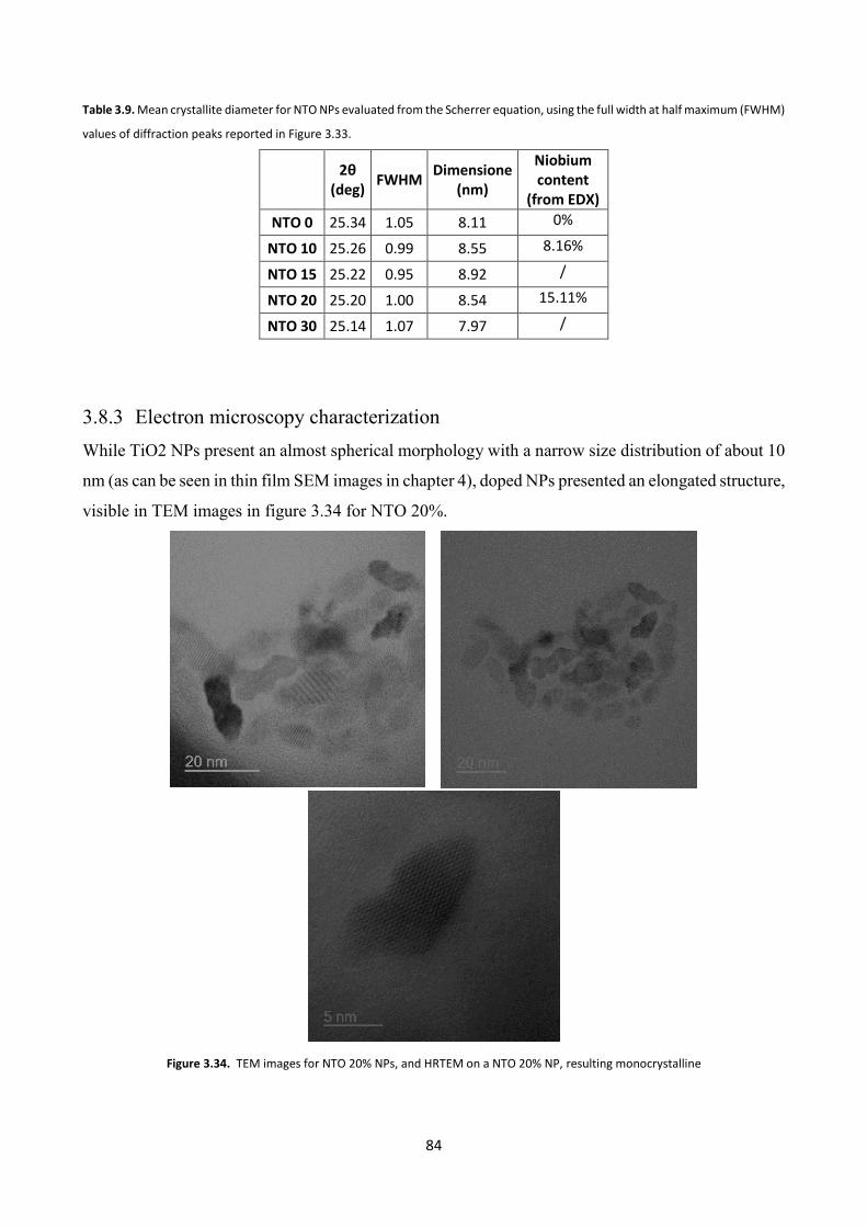
84
Table 3.9. Mean crystallite diameter for NTO NPs evaluated from the Scherrer equation, using the full width at half maximum (FWHM)
values of diffraction peaks reported in Figure 3.33.
2θ
(deg) FWHM
Dimensione (nm)
Niobium content
(from EDX)
NTO 0 25.34 1.05 8.11 0%
NTO 10 25.26 0.99 8.55 8.16%
NTO 15 25.22 0.95 8.92 /
NTO 20 25.20 1.00 8.54 15.11%
NTO 30 25.14 1.07 7.97 /
3.8.3 Electron microscopy characterization
While TiO2 NPs present an almost spherical morphology with a narrow size distribution of about 10
nm (as can be seen in thin film SEM images in chapter 4), doped NPs presented an elongated structure,
visible in TEM images in figure 3.34 for NTO 20%.
Figure 3.34. TEM images for NTO 20% NPs, and HRTEM on a NTO 20% NP, resulting monocrystalline
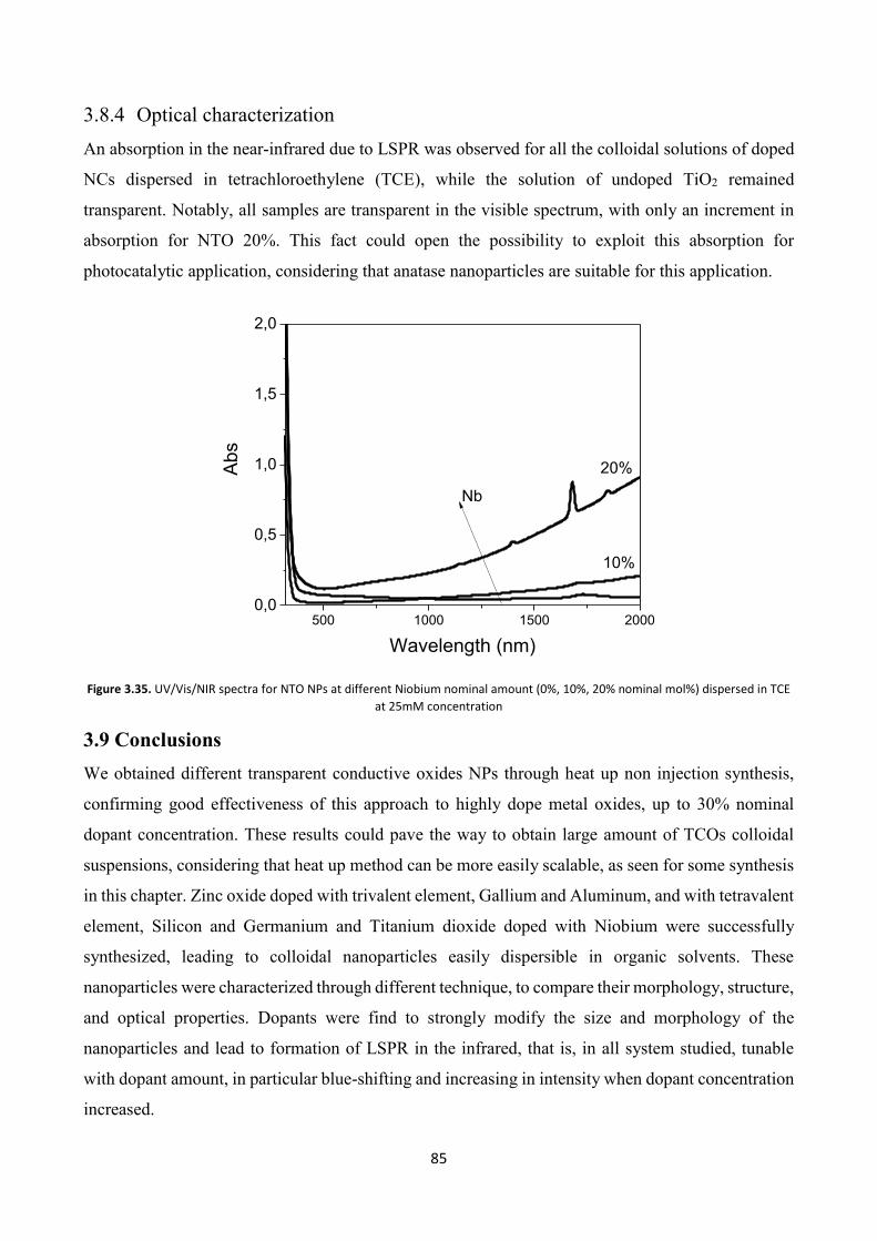
85
3.8.4 Optical characterization
An absorption in the near-infrared due to LSPR was observed for all the colloidal solutions of doped
NCs dispersed in tetrachloroethylene (TCE), while the solution of undoped TiO2 remained
transparent. Notably, all samples are transparent in the visible spectrum, with only an increment in
absorption for NTO 20%. This fact could open the possibility to exploit this absorption for
photocatalytic application, considering that anatase nanoparticles are suitable for this application.
500 1000 1500 20000,0
0,5
1,0
1,5
2,0
10%
Ab
s
Wavelength (nm)
20%
Nb
Figure 3.35. UV/Vis/NIR spectra for NTO NPs at different Niobium nominal amount (0%, 10%, 20% nominal mol%) dispersed in TCE
at 25mM concentration
3.9 Conclusions
We obtained different transparent conductive oxides NPs through heat up non injection synthesis,
confirming good effectiveness of this approach to highly dope metal oxides, up to 30% nominal
dopant concentration. These results could pave the way to obtain large amount of TCOs colloidal
suspensions, considering that heat up method can be more easily scalable, as seen for some synthesis
in this chapter. Zinc oxide doped with trivalent element, Gallium and Aluminum, and with tetravalent
element, Silicon and Germanium and Titanium dioxide doped with Niobium were successfully
synthesized, leading to colloidal nanoparticles easily dispersible in organic solvents. These
nanoparticles were characterized through different technique, to compare their morphology, structure,
and optical properties. Dopants were find to strongly modify the size and morphology of the
nanoparticles and lead to formation of LSPR in the infrared, that is, in all system studied, tunable
with dopant amount, in particular blue-shifting and increasing in intensity when dopant concentration
increased.
86
References [1] Elmer Klaus, Magnetron sputtering of transparent conductive zinc oxide: relation between the
sputtering parameters and the electronic properties, 2000 J. Phys. D: Appl. Phys.
[2] De Mello Donegá, C., Liljeroth, P. and Vanmaekelbergh, D., Physicochemical Evaluation of the
Hot-Injection Method, a Synthesis Route for Monodisperse Nanocrystals. Small, 2005, 1: 1152–
1162.
[3] Yuhas, B. D.; Zitoun, D. O.; Pauzauskie, P. J.; He, R.; Yang, P. Angew. Chem., Int. Ed. 2006, 45,
420−423
[4] Enrico Della Gaspera, Marco Bersani, Michela Cittadini, Massimo Guglielmi, Diego Pagani,
Rodrigo Noriega, Saahil Mehra, Alberto Salleo, Alessandro Martucci, Low-Temperature Processed
Ga-Doped ZnO Coatings from Colloidal Inks, J. Am. Chem. Soc. 2013, Volume 135, 3439−3448
[5] Enrico Della Gaspera, Anthony S. R. Chesman, Joel van Embden, and Jacek J. Jasieniak, Non-
injection Synthesis of Doped Zinc Oxide Plasmonic Nanocrystals, ACS Nano, 2014, 8 (9), pp 9154–
9163
[6] Luca De Trizio, Raffaella Buonsanti, Alina M. Schimpf, Anna Llordes, Daniel R. Gamelin, Roberto
Simonutti, Nb-Doped Colloidal TiO2 Nanocrystals with Tunable Infrared Absorption, and Delia J.
Milliron, Chem. Mater, 2013, 25 (16), pp 3383–3390
[7] Yongfen Chen, Myeongseob Kim, Guoda Lian, Mathew B. Johnson, and Xiaogang Peng, Side
Reactions in Controlling the Quality, Yield, and Stability of High Quality Colloidal Nanocrystals, J. Am.
Chem. Soc. 2005, 127, 13331-13337
[8] Joo, J.; Kwon, S. G.; Yu, J. H.; Hyeon, T. Synthesis of ZnO Nanocrystals with Cone, Hexagonal Cone,
and Rod Shapes via Non-hydrolytic Ester Elimination SolGel Reactions. Adv. Mater. 2005, 17, 1873–
1877.
[9] Clavel, G.; Willinger, M.-G.; Zitoun, D.; Pinna, N. Solvent Dependent Shape and Magnetic
Properties of Doped ZnO Nanostructures. Adv. Funct. Mater. 2007, 17, 3159–3169.
[10] J. Song, S. A. Kulinich, J. Li, Y. Liu and H. Zeng, Angew. Chem., Int. Ed., 2015, 54, 462–466.
[11] R. Buonsanti, A. Llordes, S. Aloni, B. A. Helms and D. J. Milliron, Nano Lett., 2011, 11, 4706–
4710.
[12] S. Ghosh, M. Saha and S. K. De, Nanoscale, 2014, 6, 7039–7051.
[13] S. Ghosh, M. Saha, V. Dev Ashok, B. Dalal and S. K. De, J. Phys. Chem. C, 2015, 119, 1180–1187.

87

88
Chapter 4
TCOs thin films characterization and
applications
4.1 Introduction
TCOs nanoparticles obtained in chapter 3 can be deposited through different techniques to produce
thin films with unique optical and electrical properties. In this chapter standard deposition method
was spin coating, in order to obtain homogeneous and uniform coating on different substrates for
different characterizations. However nothing prevents the possibility to deposit those colloidal
suspension with different deposition technique like dip coating or even spray coating to obtain large
area coating, industrializing the process. This chapter firstly will focus on the typical procedure
followed to produce TCOs thin films, briefly summarizing spin coating process theory, the
preparation of substrates and describing different steps of deposition.
Then morphological characterizations, XRD measurements and SEM images, optical
characterization, UV VIS NIR, FTIR and ellipsometric measurements, and some compositional
investigation through EDX and XPS, performed on TCOs thin films will be discussed, focusing
particularly on different behavior due to different dopant concentration.
To obtain chemically stable, conductive and functional TCOs film it is also mandatory to properly
treat the thin films; in particular some results will be presented about heat treatment in different
atmosphere (oxidizing, inert or reducing), more or less effective, leading to different film properties.
Other strategy used to treat the samples at low temperature have been exploited like UV irradiation,
trying to remove organic residues from the films, and acid attacks, to substitute long-chain ligands
with short-chain ligands, easily removable with bland heat treatments. Finally, some consideration
about applications of these films are presented, focusing on electrical property and transparency for
transparent electrode application and on optical properties in the infrared for solar control application.

89
4.2 Thin films standard deposition and treatments procedure
Before deposit thin films, the substrate underwent a series of treatments to ensure a surface clean
from any contaminated agents which may affect the thin film quality and adhesion. Subsequent
treatments, in addition, are performed to functionalize the surface making affine to the solvent used
for the deposition, allowing the production of uniform and homogeneous films. It must be stressed,
however, that the film thickness and uniformity is determined by the rheological characteristics of
the suspension, and by spinning variables (rotation speed, rotation time, initial acceleration,
atmosphere of deposition).
Process of spin coating can be summarized in four main phases, shown in figure 4.1: deposition, spin-
on, spin-off and evaporation.
Figure 4.1. Operating principle of spin coater technique. (a) deposition, (b) spin on, (c) spin off, (d) evaporation.
Deposition (a): An excess of solution is deposited in the center of the sample.
Spin-on (b): at this step starts the rotation, the acceleration can be more or less rapid depending on
the rheological properties of the solution and the desired result. It is important that not too much time
between the deposition step and the step of spin-on does not occur to prevent a premature evaporation
of the solvent from the edges of the sample. The acceleration causes a spiral vortex in the solution
deposited over the sample with the expulsion of most of the deposited liquid. At the end of the
acceleration ramp the speed remains constant.

90
Spin-off (c): the rotation speed remains constant and the film deposited thins in relation to the speed
of rotation and the viscosity of the solution deposited.
Evaporation (d): in this last phase the residual solvent is eliminated by evaporation. When using
solvents with high evaporation, this latter phase may be accelerated by placing the sample on a hot
plate at an adequate temperature for a few minutes. The rotation speed is kept constant for the
indicated time then decreases gradually until the complete stop.
The thickness of the deposited film is directly attached to several factors [ ]. A quantitative estimate
of the film thickness produced by spinning can be obtained by the equation shown below.
ℎ = (1 −𝜌𝐴0
𝜌𝐴) ∗ (
3𝜂𝑒
2𝜌𝐴0𝜔2)
1
3 (1)
where h is the final thickness of the film, ρA is the mass per unit volume of the volatile solvent, ρA0
its initial value, and the rate of evaporation of the solvent, η viscosity and ω the angular velocity. The
possible defects encountered in the spin coating technique are mainly the presence of comets and
streaks. The comets are caused by the presence of large particles or of particles of extraneous
synthesis of abnormal dimensions which hinder the flow of the solution. This type of defect can be
easily eliminated by filtering the solution, allowing to reduce the dimensional dispersion and
eliminate possible effects of scattering from the particles of greater size. The streaks are lines that
radially from a center of rotation, which are given by the different evaporation rate of the solvents on
the surface of the sample; for example, an alcohol solvent (ethanol) that have an evaporation rate
greater than water, creating a corrugated surface.
In particular, the set up used was a spin coater G3P SCS-8, and the samples were secured to the rotary
plate by the action of a vacuum pump. The substrates used were mainly silicon and SiO2 glass, square
shaped with side measuring approximately 25 mm.
The substrates underwent a chemical treatment in a basic piranha solution, consisting of H2O: NH3:
H2O2 in relations 5:1:3 (volume ratio). The samples were immersed in the solution and left for 20
minutes at 50°C. They were then thoroughly rinsed with distilled water and the surface was dried
with a vigorous stream of air, ready to be placed in the spin coater.
Thin films were usually (unless specified) produced by spin coating at 1000 rpm for 30s using TCO
dispersion in octane (~100-150 mg/ml). After spin coating, films were stabilized on a hot plate at
150°C for 15 min. This procedure was repeated many time to obtain desired film thickness. In certain
cases, the solution of the nanoparticles dispersed in octane were filtered using PTFE filters with a
pore size of 450 nm, decreasing the number of defects typical of spin coating such as comets.
Thin films were typically treated with UV irradiation layer by layer and a heat treatment in reducing
atmosphere at 450 °C (mixture of 5% H2 in Argon). Unless specified, all characterizations of TCOs
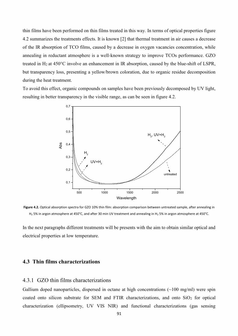
91
thin films have been performed on thin films treated in this way. In terms of optical properties figure
4.2 summarizes the treatments effects. It is known [2] that thermal treatment in air causes a decrease
of the IR absorption of TCO films, caused by a decrease in oxygen vacancies concentration, while
annealing in reductant atmosphere is a well-known strategy to improve TCOs performance. GZO
treated in H2 at 450°C involve an enhancement in IR absorption, caused by the blue-shift of LSPR,
but transparency loss, presenting a yellow/brown coloration, due to organic residue decomposition
during the heat treatment.
To avoid this effect, organic compounds on samples have been previously decomposed by UV light,
resulting in better transparency in the visible range, as can be seen in figure 4.2.
500 1000 1500 2000 2500
0,1
0,2
0,3
0,4
0,5
0,6
0,7
UV+H2
Ab
s
Wavelength
untreated
H2, UV+H
2
H2
Figure 4.2. Optical absorption spectra for GZO 10% thin film: absorption comparison between untreated sample, after annealing in
H2 5% in argon atmosphere at 450°C, and after 30 min UV treatment and annealing in H2 5% in argon atmosphere at 450°C.
In the next paragraphs different treatments will be presents with the aim to obtain similar optical and
electrical properties at low temperature.
4.3 Thin films characterizations
4.3.1 GZO thin films characterizations
Gallium doped nanoparticles, dispersed in octane at high concentrations (~100 mg/ml) were spin
coated onto silicon substrate for SEM and FTIR characterizations, and onto SiO2 for optical
characterization (ellipsometry, UV VIS NIR) and functional characterizations (gas sensing

92
measurements). For electrical sensing measurements GZO thin films were also produced onto
Si/Si3N4 supports (the top side was composed by platinum interdigitated electrodes for output
resistance signal; the back side was provided with a controlled heater circuit in order to be able to
operate in the operating temperature range 25-150°C).
Thin films were typically treated with a UV irradiation layer by layer in reducing atmosphere at 450
°C (mixture of 5% H2 in Argon). Prior to such annealing, the samples were exposed to UV light for
30 min, to remove organic compounds – mainly composed of surface ligands – and obtain purely
inorganic coatings, as previously demonstrated. The combination of UV exposure and annealing
under reducing gas atmosphere enhances the plasmonic absorption in the infrared without
compromising the transparency in the visible range.
4.3.1.1 XRD characterization
XRD patterns for GZO thin films after annealing and mean crystallite diameter calculated with
Scherrer equation are reported in figure 4.3 and Table 4.1, respectively.
20 40 60
20%
10%
5%Inte
nsity (
a.u
.)
2 (°)
0%
Figure 4.3. XRD patterns of ZnO and Gallium doped ZnO thin films. Theoretical diffraction peak positions for ZnO (JCPDS No. 36-
1451) are also reported.
Table 4.1. Mean crystallite diameter for the as-syntehsized GZO NCs and for the annealed thin films.
Sample Crystallite size (nm)
As synthesized Annealed at 450 °C
ZnO 7.5 ± 1.1 13.5 ± 2.6
GZO 5% 7.9 ± 0.8 14.2 ± 2.2
GZO 10% 10.4 ± 1.0 16.5 ± 1.6
GZO 20% 10.6 ± 1.0 15.1 ± 1.4

93
All sample present sharp peaks typical for ZnO structure. For ZnO and GZO 5%, the (100) reflection
registered at 31.8° is more intense than the tabulated value, suggesting a preferred orientation of the
lattice. Calculated mean crystallites sizes, as expected, increased with thermal annealing: average
sizes were about ~14-20 nm instead of ~7-10 nm of as prepared NPs. It’s also evident a dopant role
in the growing of the crystallites, increasing with dopant amount from 13.7 ± 0.6 for ZnO to 19.7 ±
0.9 for GZO 10%.
4.3.1.2 Electron microscopy characterization
The high quality of the GZO thin films that can be inferred from their absorption spectra is further
confirmed by microstructural analyses performed using SEM.
Figure 4.4. SEM images in plane views and cross sections for ZnO and Gallium doped zinc oxide thin films. Scale bars for upper,
central and lower panels are 1 µm, 100 nm and 500 nm, respectively.
All deposited films are uniform and homogeneous on a scale of several microns, and possess a
similar morphology regardless of the amount of dopant.
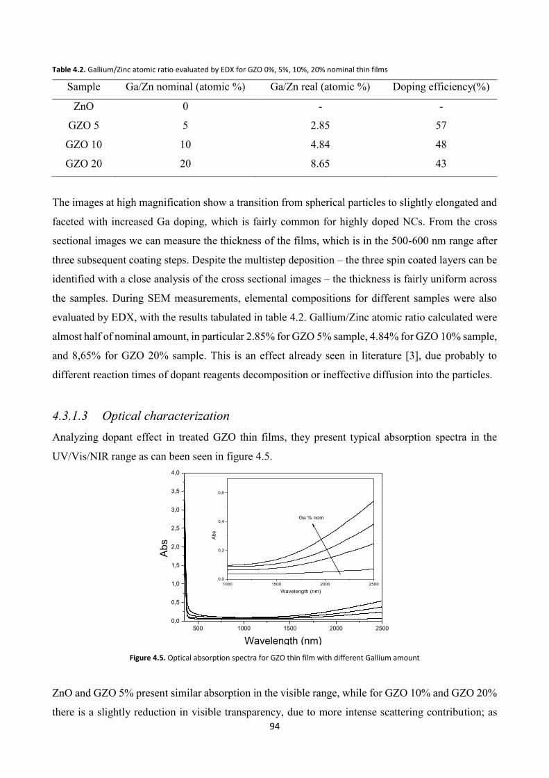
94
Table 4.2. Gallium/Zinc atomic ratio evaluated by EDX for GZO 0%, 5%, 10%, 20% nominal thin films
Sample Ga/Zn nominal (atomic %) Ga/Zn real (atomic %) Doping efficiency(%)
ZnO 0 - -
GZO 5 5 2.85 57
GZO 10 10 4.84 48
GZO 20 20 8.65 43
The images at high magnification show a transition from spherical particles to slightly elongated and
faceted with increased Ga doping, which is fairly common for highly doped NCs. From the cross
sectional images we can measure the thickness of the films, which is in the 500-600 nm range after
three subsequent coating steps. Despite the multistep deposition – the three spin coated layers can be
identified with a close analysis of the cross sectional images – the thickness is fairly uniform across
the samples. During SEM measurements, elemental compositions for different samples were also
evaluated by EDX, with the results tabulated in table 4.2. Gallium/Zinc atomic ratio calculated were
almost half of nominal amount, in particular 2.85% for GZO 5% sample, 4.84% for GZO 10% sample,
and 8,65% for GZO 20% sample. This is an effect already seen in literature [3], due probably to
different reaction times of dopant reagents decomposition or ineffective diffusion into the particles.
4.3.1.3 Optical characterization
Analyzing dopant effect in treated GZO thin films, they present typical absorption spectra in the
UV/Vis/NIR range as can been seen in figure 4.5.
500 1000 1500 2000 2500
0,0
0,5
1,0
1,5
2,0
2,5
3,0
3,5
4,0
1000 1500 2000 2500
0,0
0,2
0,4
0,6
Abs
(a.u
.)
Wavelength (nm)
Ga % nom
Abs
Wavelength (nm)
Figure 4.5. Optical absorption spectra for GZO thin film with different Gallium amount
ZnO and GZO 5% present similar absorption in the visible range, while for GZO 10% and GZO 20%
there is a slightly reduction in visible transparency, due to more intense scattering contribution; as
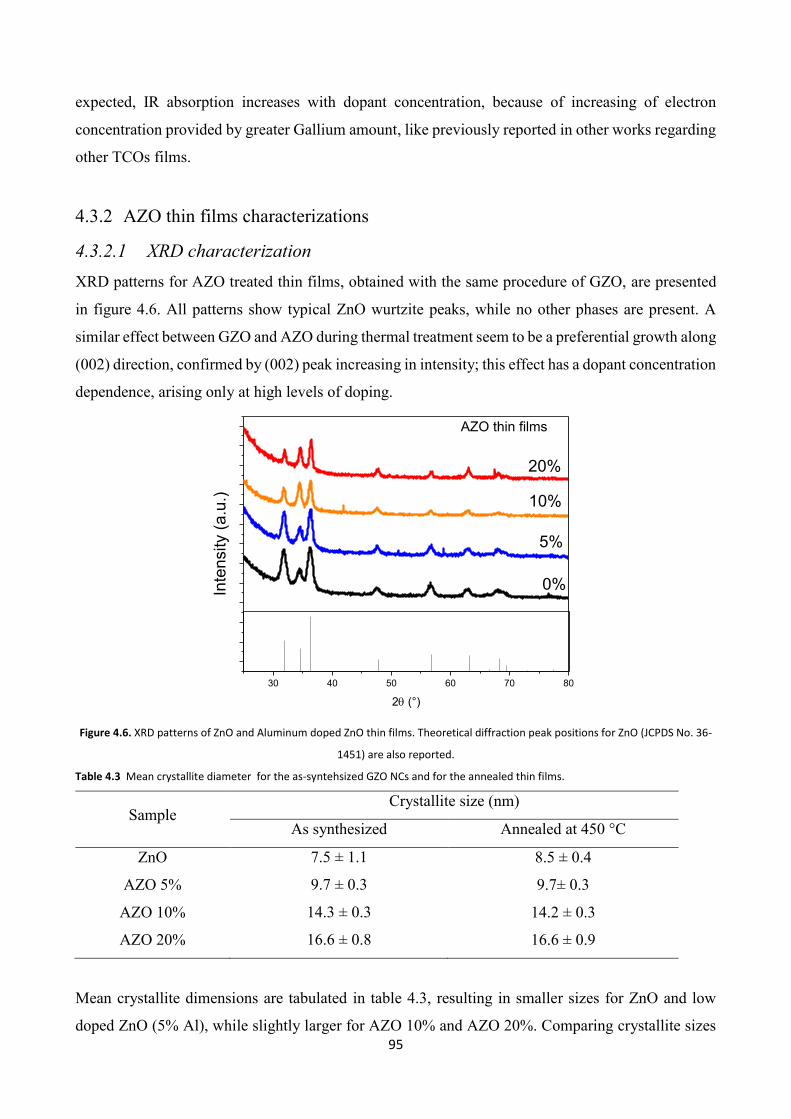
95
expected, IR absorption increases with dopant concentration, because of increasing of electron
concentration provided by greater Gallium amount, like previously reported in other works regarding
other TCOs films.
4.3.2 AZO thin films characterizations
4.3.2.1 XRD characterization
XRD patterns for AZO treated thin films, obtained with the same procedure of GZO, are presented
in figure 4.6. All patterns show typical ZnO wurtzite peaks, while no other phases are present. A
similar effect between GZO and AZO during thermal treatment seem to be a preferential growth along
(002) direction, confirmed by (002) peak increasing in intensity; this effect has a dopant concentration
dependence, arising only at high levels of doping.
30 40 50 60 70 80
20%
10%
5%
Inte
nsity (
a.u
.)
2 (°)
AZO thin films
0%
Figure 4.6. XRD patterns of ZnO and Aluminum doped ZnO thin films. Theoretical diffraction peak positions for ZnO (JCPDS No. 36-
1451) are also reported.
Table 4.3 Mean crystallite diameter for the as-syntehsized GZO NCs and for the annealed thin films.
Sample Crystallite size (nm)
As synthesized Annealed at 450 °C
ZnO 7.5 ± 1.1 8.5 ± 0.4
AZO 5% 9.7 ± 0.3 9.7± 0.3
AZO 10% 14.3 ± 0.3 14.2 ± 0.3
AZO 20% 16.6 ± 0.8 16.6 ± 0.9
Mean crystallite dimensions are tabulated in table 4.3, resulting in smaller sizes for ZnO and low
doped ZnO (5% Al), while slightly larger for AZO 10% and AZO 20%. Comparing crystallite sizes
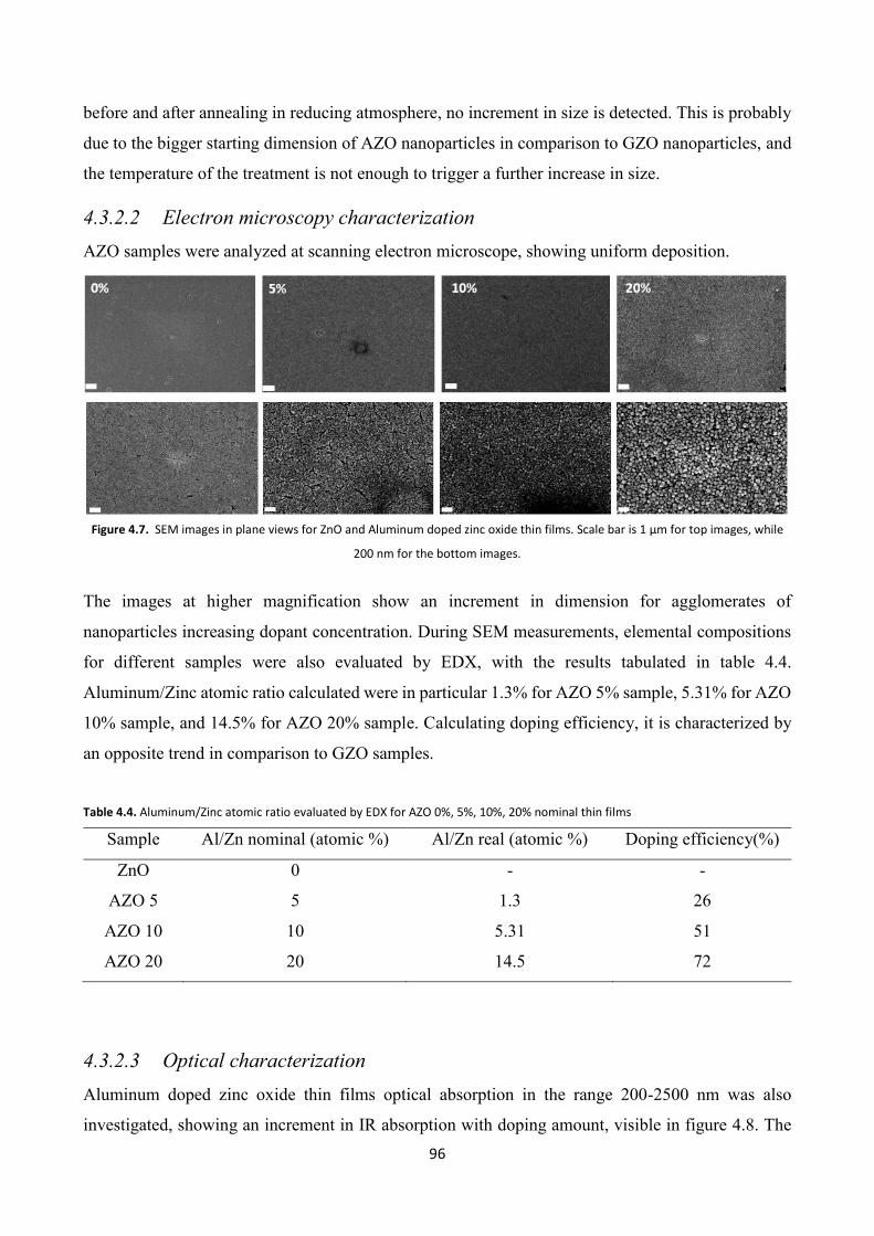
96
before and after annealing in reducing atmosphere, no increment in size is detected. This is probably
due to the bigger starting dimension of AZO nanoparticles in comparison to GZO nanoparticles, and
the temperature of the treatment is not enough to trigger a further increase in size.
4.3.2.2 Electron microscopy characterization
AZO samples were analyzed at scanning electron microscope, showing uniform deposition.
Figure 4.7. SEM images in plane views for ZnO and Aluminum doped zinc oxide thin films. Scale bar is 1 µm for top images, while
200 nm for the bottom images.
The images at higher magnification show an increment in dimension for agglomerates of
nanoparticles increasing dopant concentration. During SEM measurements, elemental compositions
for different samples were also evaluated by EDX, with the results tabulated in table 4.4.
Aluminum/Zinc atomic ratio calculated were in particular 1.3% for AZO 5% sample, 5.31% for AZO
10% sample, and 14.5% for AZO 20% sample. Calculating doping efficiency, it is characterized by
an opposite trend in comparison to GZO samples.
Table 4.4. Aluminum/Zinc atomic ratio evaluated by EDX for AZO 0%, 5%, 10%, 20% nominal thin films
Sample Al/Zn nominal (atomic %) Al/Zn real (atomic %) Doping efficiency(%)
ZnO 0 - -
AZO 5 5 1.3 26
AZO 10 10 5.31 51
AZO 20 20 14.5 72
4.3.2.3 Optical characterization
Aluminum doped zinc oxide thin films optical absorption in the range 200-2500 nm was also
investigated, showing an increment in IR absorption with doping amount, visible in figure 4.8. The
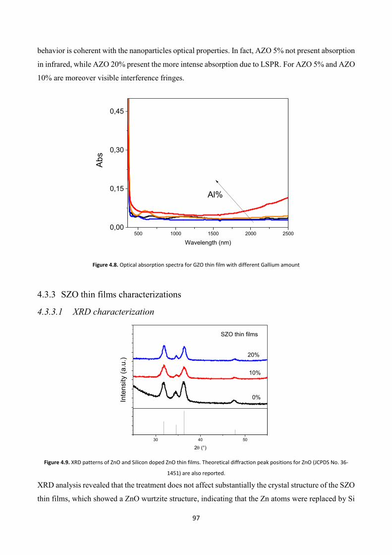
97
behavior is coherent with the nanoparticles optical properties. In fact, AZO 5% not present absorption
in infrared, while AZO 20% present the more intense absorption due to LSPR. For AZO 5% and AZO
10% are moreover visible interference fringes.
500 1000 1500 2000 25000,00
0,15
0,30
0,45
Ab
s
Wavelength (nm)
Al%
Figure 4.8. Optical absorption spectra for GZO thin film with different Gallium amount
4.3.3 SZO thin films characterizations
4.3.3.1 XRD characterization
30 40 50
20%
10%
Inte
nsity (
a.u
.)
2 (°)
0%
SZO thin films
Figure 4.9. XRD patterns of ZnO and Silicon doped ZnO thin films. Theoretical diffraction peak positions for ZnO (JCPDS No. 36-
1451) are also reported.
XRD analysis revealed that the treatment does not affect substantially the crystal structure of the SZO
thin films, which showed a ZnO wurtzite structure, indicating that the Zn atoms were replaced by Si
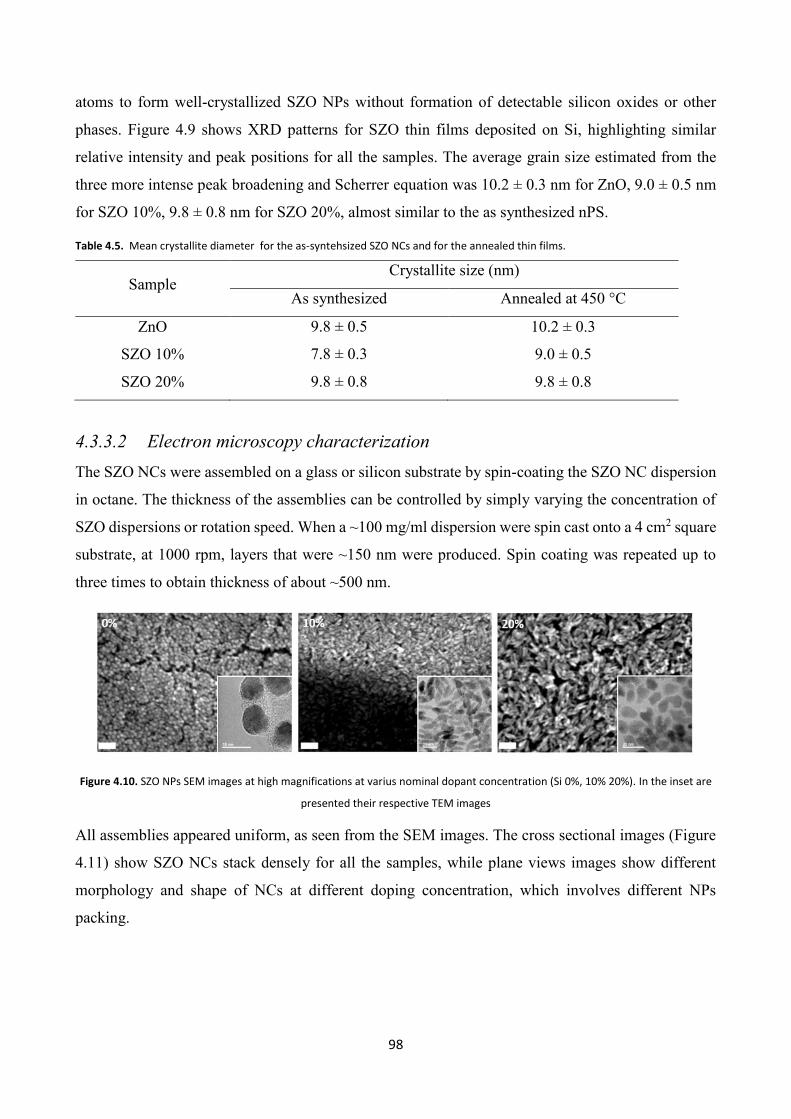
98
atoms to form well-crystallized SZO NPs without formation of detectable silicon oxides or other
phases. Figure 4.9 shows XRD patterns for SZO thin films deposited on Si, highlighting similar
relative intensity and peak positions for all the samples. The average grain size estimated from the
three more intense peak broadening and Scherrer equation was 10.2 ± 0.3 nm for ZnO, 9.0 ± 0.5 nm
for SZO 10%, 9.8 ± 0.8 nm for SZO 20%, almost similar to the as synthesized nPS.
Table 4.5. Mean crystallite diameter for the as-syntehsized SZO NCs and for the annealed thin films.
Sample Crystallite size (nm)
As synthesized Annealed at 450 °C
ZnO 9.8 ± 0.5 10.2 ± 0.3
SZO 10% 7.8 ± 0.3 9.0 ± 0.5
SZO 20% 9.8 ± 0.8 9.8 ± 0.8
4.3.3.2 Electron microscopy characterization
The SZO NCs were assembled on a glass or silicon substrate by spin-coating the SZO NC dispersion
in octane. The thickness of the assemblies can be controlled by simply varying the concentration of
SZO dispersions or rotation speed. When a ~100 mg/ml dispersion were spin cast onto a 4 cm2 square
substrate, at 1000 rpm, layers that were ~150 nm were produced. Spin coating was repeated up to
three times to obtain thickness of about ~500 nm.
Figure 4.10. SZO NPs SEM images at high magnifications at varius nominal dopant concentration (Si 0%, 10% 20%). In the inset are
presented their respective TEM images
All assemblies appeared uniform, as seen from the SEM images. The cross sectional images (Figure
4.11) show SZO NCs stack densely for all the samples, while plane views images show different
morphology and shape of NCs at different doping concentration, which involves different NPs
packing.
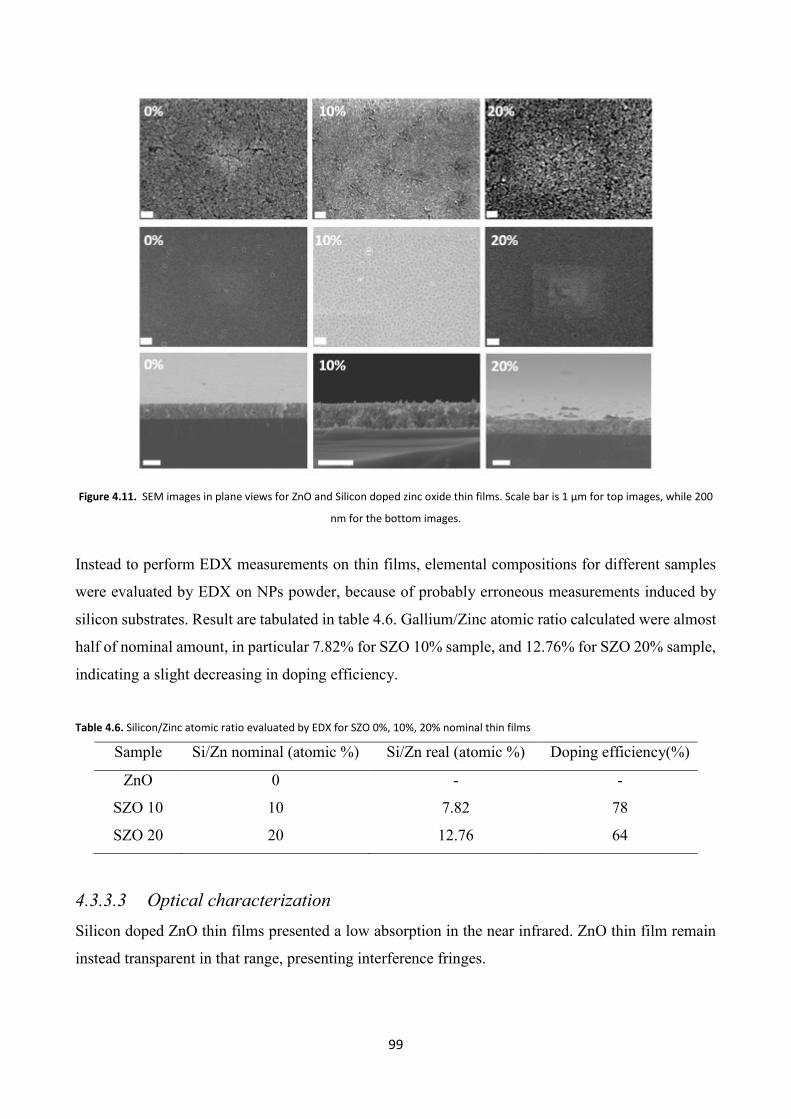
99
Figure 4.11. SEM images in plane views for ZnO and Silicon doped zinc oxide thin films. Scale bar is 1 µm for top images, while 200
nm for the bottom images.
Instead to perform EDX measurements on thin films, elemental compositions for different samples
were evaluated by EDX on NPs powder, because of probably erroneous measurements induced by
silicon substrates. Result are tabulated in table 4.6. Gallium/Zinc atomic ratio calculated were almost
half of nominal amount, in particular 7.82% for SZO 10% sample, and 12.76% for SZO 20% sample,
indicating a slight decreasing in doping efficiency.
Table 4.6. Silicon/Zinc atomic ratio evaluated by EDX for SZO 0%, 10%, 20% nominal thin films
Sample Si/Zn nominal (atomic %) Si/Zn real (atomic %) Doping efficiency(%)
ZnO 0 - -
SZO 10 10 7.82 78
SZO 20 20 12.76 64
4.3.3.3 Optical characterization
Silicon doped ZnO thin films presented a low absorption in the near infrared. ZnO thin film remain
instead transparent in that range, presenting interference fringes.
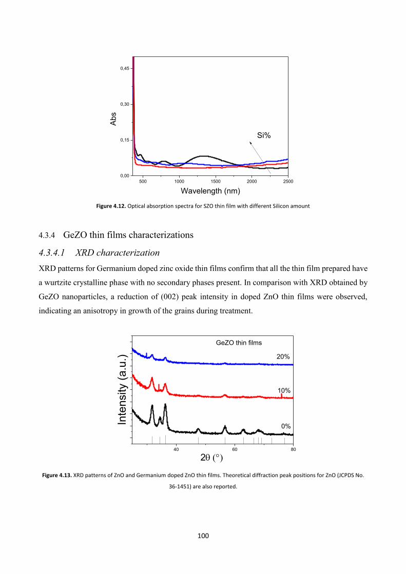
100
500 1000 1500 2000 2500
0,00
0,15
0,30
0,45
Abs
Wavelength (nm)
Si%
Figure 4.12. Optical absorption spectra for SZO thin film with different Silicon amount
4.3.4 GeZO thin films characterizations
4.3.4.1 XRD characterization
XRD patterns for Germanium doped zinc oxide thin films confirm that all the thin film prepared have
a wurtzite crystalline phase with no secondary phases present. In comparison with XRD obtained by
GeZO nanoparticles, a reduction of (002) peak intensity in doped ZnO thin films were observed,
indicating an anisotropy in growth of the grains during treatment.
40 60 80
0%
10%
Inte
nsity (
a.u
.)
2
GeZO thin films
20%
Figure 4.13. XRD patterns of ZnO and Germanium doped ZnO thin films. Theoretical diffraction peak positions for ZnO (JCPDS No.
36-1451) are also reported.

101
This effect can be ascribed to the growing of elongated structures, confirmed by SEM images of thin films
presented in next paragraph. The crystallite diameter evaluated with the Scherrer equation for thin films was
almost the same of nanoparticles and it is reported in table 4.7 for comparison.
Table 4.7. Mean crystallite diameter for the as-syntehsized GeZO NCs and for the annealed thin films.
Sample Crystallite size (nm)
As synthesized Annealed at 450 °C
ZnO 7.5 ± 1.1 8.9 ± 1.0
GeZO 10% 11.9 ± 4.8 10.4 ± 3.5
GeZO 20% 12.4 ± 2.3 12.8 ± 2.0
4.3.4.2 Electron microscopy and XPS characterizations
SEM images for Germanium doped zinc oxide and undoped zinc oxide are presented in figure 4.14,
at different magnifications. Different morphology of nanoparticles are evident at 500000x
magnification, with spherical shape for undoped ZnO, while elongated shape for Germanium doped
ZnO.
Figure 4.14. SEM images in plane views for ZnO and Germanium doped zinc oxide thin films. Scale bars for upper and lower panels
are 1 µm and 100 nm respectively.
Table 4.8. Germanium/Zinc atomic ratio evaluated by EDX for GeZO 0%, 10%, 20% nominal thin films
Sample Ge/Zn nominal (atomic %) Ge/Zn real (atomic %) Doping efficiency(%)
ZnO 0 - -
GeZO 10 10 9.33 93
GeZO 20 20 13.48 67

102
Germanium/Zinc ratio were evaluated by EDX for doped sample, showing high doping efficiency for
GeZO 10% (93%), while efficiency lower for GeZO 20% (67%). XPS measurement were also
performed on GeZO 10% and GeZO 20% thin films to evaluate oxidation state for Ge ions in ZnO
crystals. XPS confirm the presence of Ge ions, predominantly in oxidation state Ge4+, indicating the
dopant role of Germanium in substitution of the bivalent element Zn2+.
Moreover, although it is not possible to quantitatively confirm the exact amount of Germanium, it is
possible to make a qualitative observation, that is GeZO 20% not presents double amount of
Germanium in respect to GeZO 10%, but only a slightly higher amount. This is quite coherent with
EDX measurement, and the doping efficiency calculated for the two different synthesis.
Figure 4.15. XPS measurement for Germanium doped zinc oxide thin films. In the bottom, survey for GeZO 10% and GeZO 20%, on
the top, Zn2p for GeZO 10% and GeZO 20%
4.3.4.3 Optical characterization
Germanium doped Zinc oxide thin films present high transparency in the visible, while absorption in
the near IR due to the tail of LSPR is quite evident, as reported in figure
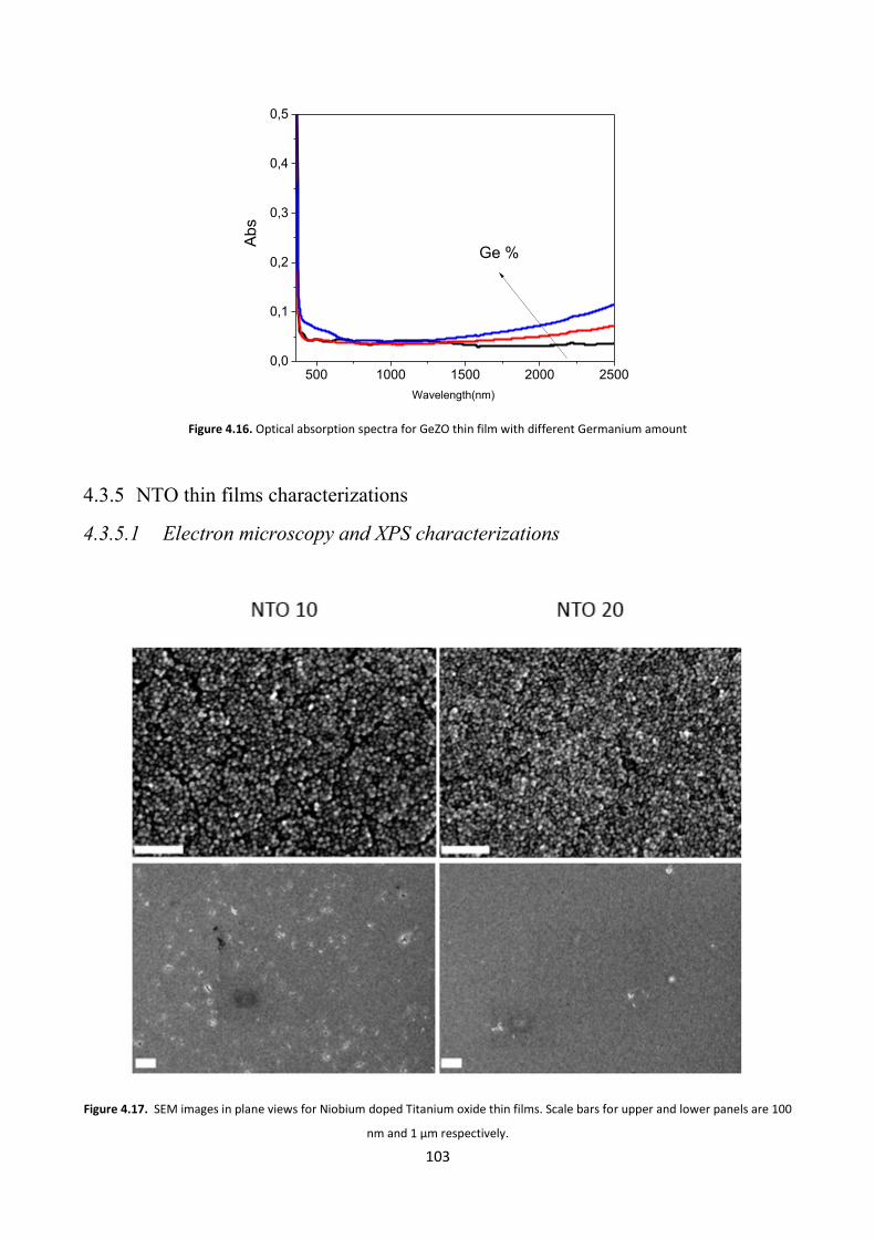
103
500 1000 1500 2000 25000,0
0,1
0,2
0,3
0,4
0,5
Abs
Wavelength(nm)
Ge %
Figure 4.16. Optical absorption spectra for GeZO thin film with different Germanium amount
4.3.5 NTO thin films characterizations
4.3.5.1 Electron microscopy and XPS characterizations
Figure 4.17. SEM images in plane views for Niobium doped Titanium oxide thin films. Scale bars for upper and lower panels are 100
nm and 1 µm respectively.
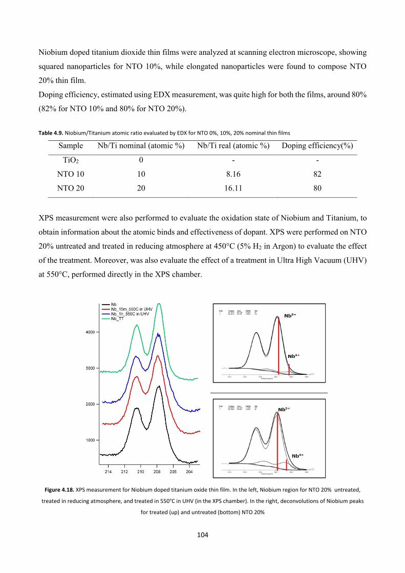
104
Niobium doped titanium dioxide thin films were analyzed at scanning electron microscope, showing
squared nanoparticles for NTO 10%, while elongated nanoparticles were found to compose NTO
20% thin film.
Doping efficiency, estimated using EDX measurement, was quite high for both the films, around 80%
(82% for NTO 10% and 80% for NTO 20%).
Table 4.9. Niobium/Titanium atomic ratio evaluated by EDX for NTO 0%, 10%, 20% nominal thin films
Sample Nb/Ti nominal (atomic %) Nb/Ti real (atomic %) Doping efficiency(%)
TiO2 0 - -
NTO 10 10 8.16 82
NTO 20 20 16.11 80
XPS measurement were also performed to evaluate the oxidation state of Niobium and Titanium, to
obtain information about the atomic binds and effectiveness of dopant. XPS were performed on NTO
20% untreated and treated in reducing atmosphere at 450°C (5% H2 in Argon) to evaluate the effect
of the treatment. Moreover, was also evaluate the effect of a treatment in Ultra High Vacuum (UHV)
at 550°C, performed directly in the XPS chamber.
Figure 4.18. XPS measurement for Niobium doped titanium oxide thin film. In the left, Niobium region for NTO 20% untreated,
treated in reducing atmosphere, and treated in 550°C in UHV (in the XPS chamber). In the right, deconvolutions of Niobium peaks
for treated (up) and untreated (bottom) NTO 20%
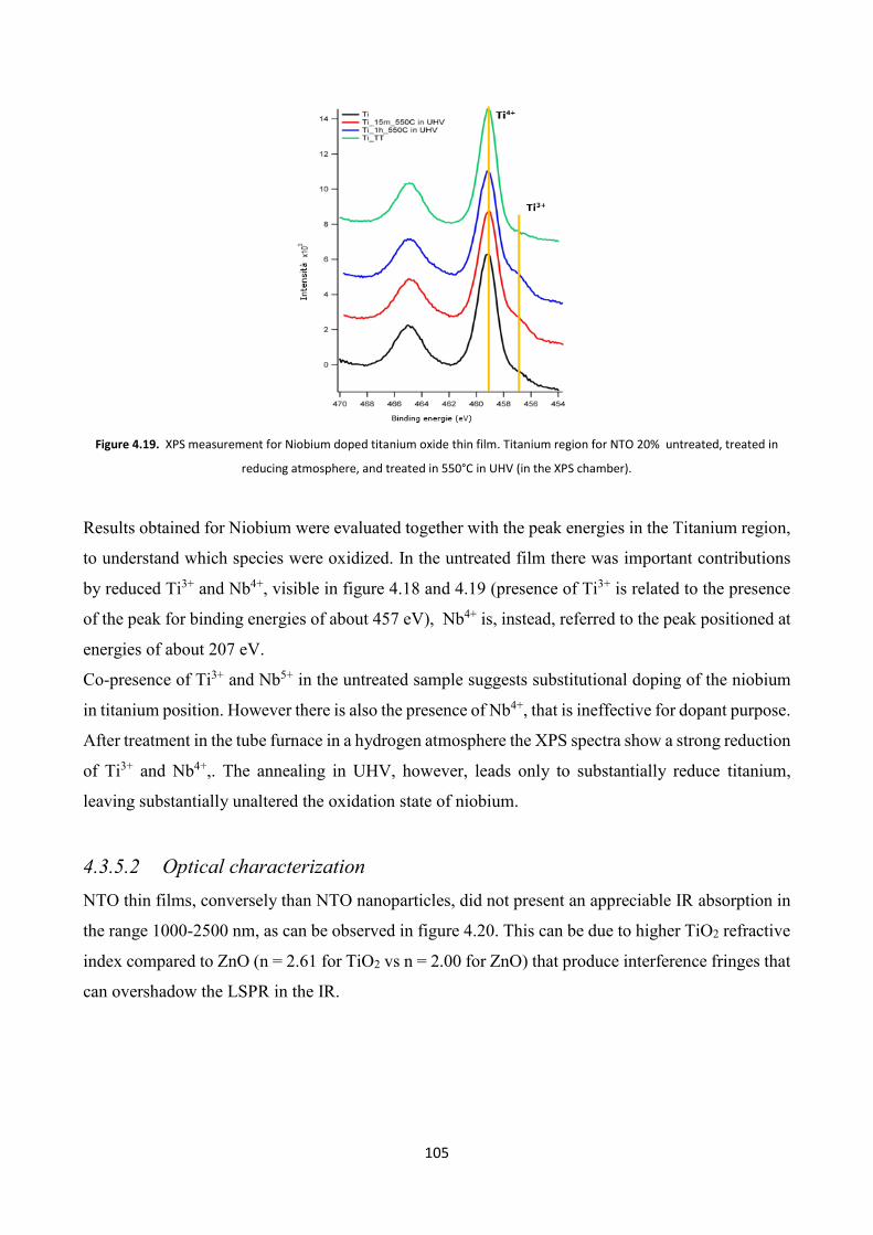
105
Figure 4.19. XPS measurement for Niobium doped titanium oxide thin film. Titanium region for NTO 20% untreated, treated in
reducing atmosphere, and treated in 550°C in UHV (in the XPS chamber).
Results obtained for Niobium were evaluated together with the peak energies in the Titanium region,
to understand which species were oxidized. In the untreated film there was important contributions
by reduced Ti3+ and Nb4+, visible in figure 4.18 and 4.19 (presence of Ti3+ is related to the presence
of the peak for binding energies of about 457 eV), Nb4+ is, instead, referred to the peak positioned at
energies of about 207 eV.
Co-presence of Ti3+ and Nb5+ in the untreated sample suggests substitutional doping of the niobium
in titanium position. However there is also the presence of Nb4+, that is ineffective for dopant purpose.
After treatment in the tube furnace in a hydrogen atmosphere the XPS spectra show a strong reduction
of Ti3+ and Nb4+,. The annealing in UHV, however, leads only to substantially reduce titanium,
leaving substantially unaltered the oxidation state of niobium.
4.3.5.2 Optical characterization
NTO thin films, conversely than NTO nanoparticles, did not present an appreciable IR absorption in
the range 1000-2500 nm, as can be observed in figure 4.20. This can be due to higher TiO2 refractive
index compared to ZnO (n = 2.61 for TiO2 vs n = 2.00 for ZnO) that produce interference fringes that
can overshadow the LSPR in the IR.
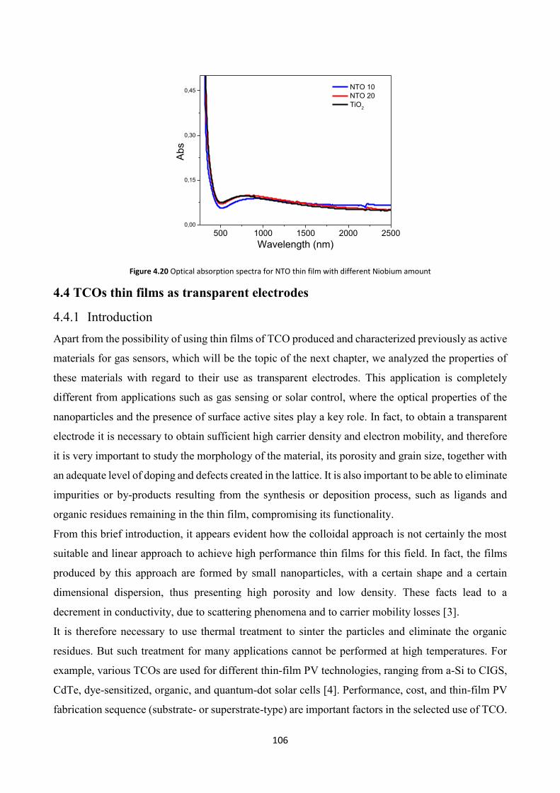
106
500 1000 1500 2000 25000,00
0,15
0,30
0,45 NTO 10
NTO 20
TiO2
Abs
Wavelength (nm)
Figure 4.20 Optical absorption spectra for NTO thin film with different Niobium amount
4.4 TCOs thin films as transparent electrodes
4.4.1 Introduction
Apart from the possibility of using thin films of TCO produced and characterized previously as active
materials for gas sensors, which will be the topic of the next chapter, we analyzed the properties of
these materials with regard to their use as transparent electrodes. This application is completely
different from applications such as gas sensing or solar control, where the optical properties of the
nanoparticles and the presence of surface active sites play a key role. In fact, to obtain a transparent
electrode it is necessary to obtain sufficient high carrier density and electron mobility, and therefore
it is very important to study the morphology of the material, its porosity and grain size, together with
an adequate level of doping and defects created in the lattice. It is also important to be able to eliminate
impurities or by-products resulting from the synthesis or deposition process, such as ligands and
organic residues remaining in the thin film, compromising its functionality.
From this brief introduction, it appears evident how the colloidal approach is not certainly the most
suitable and linear approach to achieve high performance thin films for this field. In fact, the films
produced by this approach are formed by small nanoparticles, with a certain shape and a certain
dimensional dispersion, thus presenting high porosity and low density. These facts lead to a
decrement in conductivity, due to scattering phenomena and to carrier mobility losses [3].
It is therefore necessary to use thermal treatment to sinter the particles and eliminate the organic
residues. But such treatment for many applications cannot be performed at high temperatures. For
example, various TCOs are used for different thin-film PV technologies, ranging from a-Si to CIGS,
CdTe, dye-sensitized, organic, and quantum-dot solar cells [4]. Performance, cost, and thin-film PV
fabrication sequence (substrate- or superstrate-type) are important factors in the selected use of TCO.
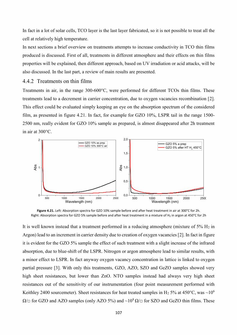
107
In fact in a lot of solar cells, TCO layer is the last layer fabricated, so it is not possible to treat all the
cell at relatively high temperature.
In next sections a brief overview on treatments attempts to increase conductivity in TCO thin films
produced is discussed. First of all, treatments in different atmosphere and their effects on thin films
properties will be explained, then different approach, based on UV irradiation or acid attacks, will be
also discussed. In the last part, a review of main results are presented.
4.4.2 Treatments on thin films
Treatments in air, in the range 300-600°C, were performed for different TCOs thin films. These
treatments lead to a decrement in carrier concentration, due to oxygen vacancies recombination [2].
This effect could be evaluated simply keeping an eye on the absorption spectrum of the considered
film, as presented in figure 4.21. In fact, for example for GZO 10%, LSPR tail in the range 1500-
2500 nm, really evident for GZO 10% sample as prepared, is almost disappeared after 2h treatment
in air at 300°C.
500 1000 1500 2000 25000
1
2
Ab
s
Wavelength (nm)
GZO 10% as prep
GZO 10% 300°C air
500 1000 1500 2000 25000,0
0,5
1,0
1,5
2,0
Ab
s
Wavelength (nm)
GZO 5% a prep
GZO 5% after HT H2 450°C
Figure 4.21. Left: Absorption spectra for GZO 10% sample before and after heat treatment in air at 300°C for 2h.
Right: Absorption spectra for GZO 5% sample before and after heat treatment in a mixture of H2 in argon at 450°C for 2h
It is well known instead that a treatment performed in a reducing atmosphere (mixture of 5% H2 in
Argon) lead to an increment in carrier density due to creation of oxygen vacancies [2]. In fact in figure
it is evident for the GZO 5% sample the effect of such treatment with a slight increase of the infrared
absorption, due to blue-shift of the LSPR. Nitrogen or argon atmosphere lead to similar results, with
a minor effect to LSPR. In fact anyway oxygen vacancy concentration in lattice is linked to oxygen
partial pressure [3]. With only this treatments, GZO, AZO, SZO and GeZO samples showed very
high sheet resistances, but lower than ZnO. NTO samples instead had always very high sheet
resistances out of the sensitivity of our instrumentation (four point measurement performed with
Keithley 2400 sourcemeter). Sheet resistances for heat treated samples in H2 5% at 450°C, was ~106
Ω/□ for GZO and AZO samples (only AZO 5%) and ~108 Ω/□ for SZO and GeZO thin films. These

108
values are too high for electrode applications, however our colloidal suspensions, with those
resistances, could be used coupled with silver nanowires, to ensure their stability and guarantee
tridimensional conduction, a strategy recently studied [5]. For this application, calculation and models
assure that a thin film with ~106 Ω/□ is enough to obtain a functional device [6]. However, a
secondary effect of the treatment in reducing of inert atmosphere was that in visible range thin films
became less transparent. This result was attributed to organic residues due to partial combustion due
to oxygen deficiency atmosphere.
To overcome that effect some other approaches were tempted. First of all, we tried to decompose
organic residue prior to heat treatment by illuminating thin films with UV irradiation. Zinc Oxide and
Titanium Oxide (in anatase phase, like our particles) possess moreover photocatalytic activity [7],
that can further enhance UV irradiation effect.
To evaluate and optimize the UV treatment some FTIR studies were performed. In figure 4.22, FTIR
spectra, in the range 2800 – 3000 cm-1, show decreasing of characteristic peaks of C-H bond stretch,
indicating the degradation of organic materials on the film.
Figure 4.22. FTIR absorption spectra for ZnO under UV irradiation after different time
500 1000 1500 2000 25000,0
0,5
1,0
1,5
2,0
Abs
Wavelength (nm)
GZO 5% a prep
GZO 5% after HT H2 450°C
500 1000 1500 2000 25000,0
0,5
1,0
1,5
2,0
Ab
s
Wavelength (nm)
GZO 5% as prep
GZO 5% after UV and HT H2 450°C
Figure 4.23. Left: Absorption spectra for GZO 5% sample before and after heat treatment in a mixture of H2 in argon at 450°C for
2h. Right: Absorption spectra for GZO 5% sample before and after UV treatment and heat treatment in a mixture of H2 in argon at
450°C for 2h

109
Performing such UV treatments before heat treatment lead to a restored transparency in the visible,
maintaining IR absorption due to LSPR, like in figure, showed with figure 4.23 for comparison.
As well as removing organic, UV irradiation was found to temporarily blue shift the IR LSPR, and
to modify band gap energy, effect well known effect for ZnO material [8].
In addition another approach was studied, consisting in ligands exchange through organic acid
attacks, in order to substitute long-chain ligands (oleate) with short-chain ligands, more easily
removable. We decided to use oxalic acid, which was found pretty aggressive to remove oleate
ligands from PbSe QD thin films [9]. To elucidate the impact of oxalic acid treatment on TCOs thin
films we monitored the impact of the attack through FTIR spectroscopy measurements, observing
characteristic peaks for different organic ligands and quantify the displacement of oleate. Presumably
this ligand exchange occurs by protonation of oleate by the free short-chain acids, resulting in
desorption of oleic acid and adsorption, to varying degrees, of oxalate ligands.
Oxalic acid was added in acetonitrile (0.1 M) and the thin films were immersed in that solution for 5
minutes. After that, the thin films were rinsed with pure acetonitrile and then with ethanol, and finally
dried. This method was found to remove essentially all of the original oleate from the surface of the
film, as determined from C-H stretch intensities (at 2915 cm-1 and at 2850 cm-1) decreasing in the
FTIR spectra (see figure 4.24), and adds a substantial amount of oxalate to the film, signaled by the
appearance of strong -COO vibrations at 1612 and 1294 cm-1 [9].
Figure 4.24. FTIR absorption spectra for ZnO before and after treatment in oxalic acid (0,1 M in acetonitrile) at room temperature.
It is evident the decrement in C-H stretch intensity and a new peak corresponding to –COO vibrations
After this satisfactory results, it was also mandatory to evaluate acid attack effects, in order to
understand if it involved changes in other crucial properties. In figure 4.25 are presented the optical
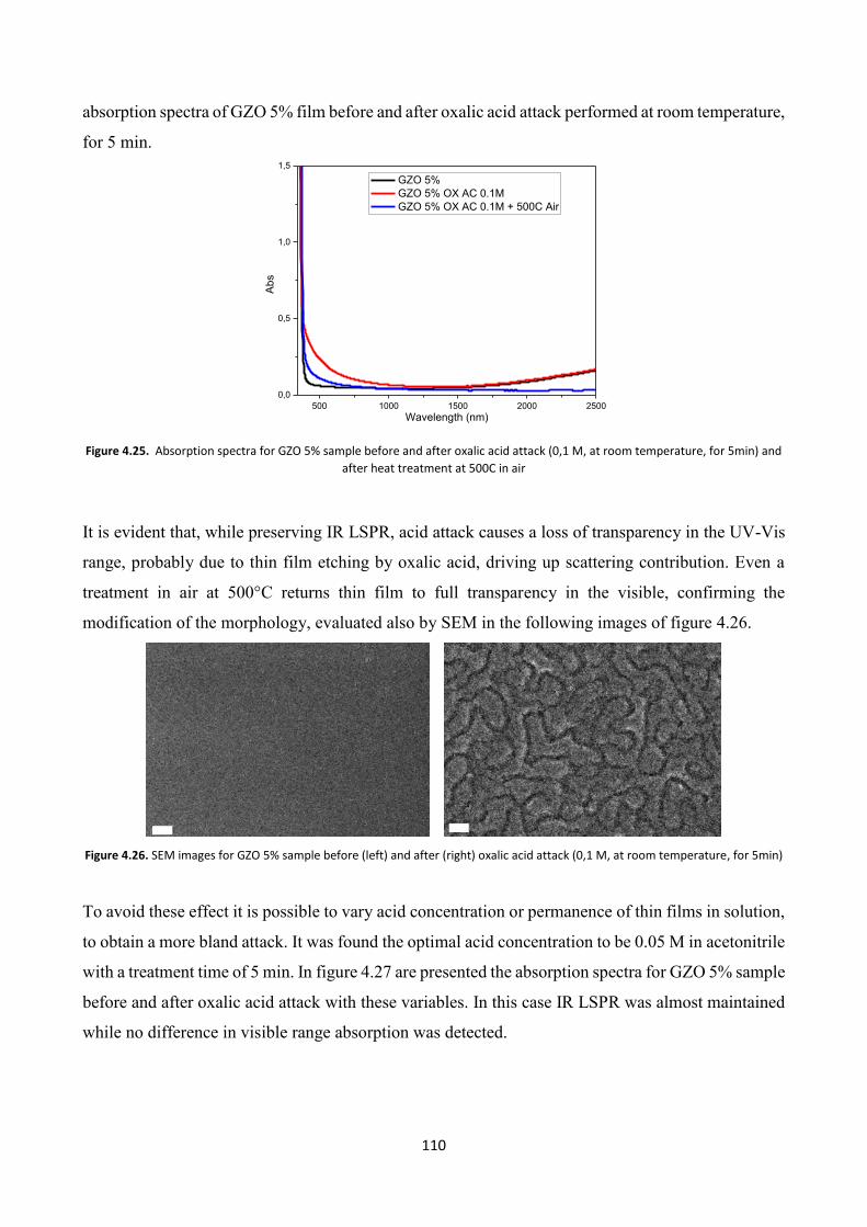
110
absorption spectra of GZO 5% film before and after oxalic acid attack performed at room temperature,
for 5 min.
500 1000 1500 2000 2500
0,0
0,5
1,0
1,5
Ab
s
Wavelength (nm)
GZO 5%
GZO 5% OX AC 0.1M
GZO 5% OX AC 0.1M + 500C Air
Figure 4.25. Absorption spectra for GZO 5% sample before and after oxalic acid attack (0,1 M, at room temperature, for 5min) and
after heat treatment at 500C in air
It is evident that, while preserving IR LSPR, acid attack causes a loss of transparency in the UV-Vis
range, probably due to thin film etching by oxalic acid, driving up scattering contribution. Even a
treatment in air at 500°C returns thin film to full transparency in the visible, confirming the
modification of the morphology, evaluated also by SEM in the following images of figure 4.26.
Figure 4.26. SEM images for GZO 5% sample before (left) and after (right) oxalic acid attack (0,1 M, at room temperature, for 5min)
To avoid these effect it is possible to vary acid concentration or permanence of thin films in solution,
to obtain a more bland attack. It was found the optimal acid concentration to be 0.05 M in acetonitrile
with a treatment time of 5 min. In figure 4.27 are presented the absorption spectra for GZO 5% sample
before and after oxalic acid attack with these variables. In this case IR LSPR was almost maintained
while no difference in visible range absorption was detected.

111
500 1000 1500 2000 25000,0
0,5
1,0
1,5
2,0
Abs
Wavelength (nm)
GZO 5% as prep
GZO 5% 0.05M 5min
Figure 4.27 Absorption spectra for GZO 5% sample before and after oxalic acid attack (0,05 M, at room temperature, for 5min)
4.4.3 Electro-optical characterization
The main results concerning the electrical and optical properties of TCOs thin films prepared in this
work are summarized in this paragraph. The best sample in terms of sheet resistance values was found
to be GZO 10%. In figure 4.28, are reported the main characterizations for GZO 10%, in particular
sheet resistances was lowered using UV and oxalic acid treatments of one order of magnitude, passing
from ~140kΩ/□ for sample treated in reducing atmosphere (H2 5% in Argon at 450°C)
Figure 4.28. a) Sheet resistances measured for GZO 10% thin film treated in reducing atmosphere, treated with UV and reducing
atmosphere, and treated with oxalic acid, UV and reducing atmosphere. b) Absorption spectra for ZnO and GZO 10% samples after
reducing treatment c) SEM image of GZO 10%, plane view (500000x) d) SEM image of GZO 10%, cross section
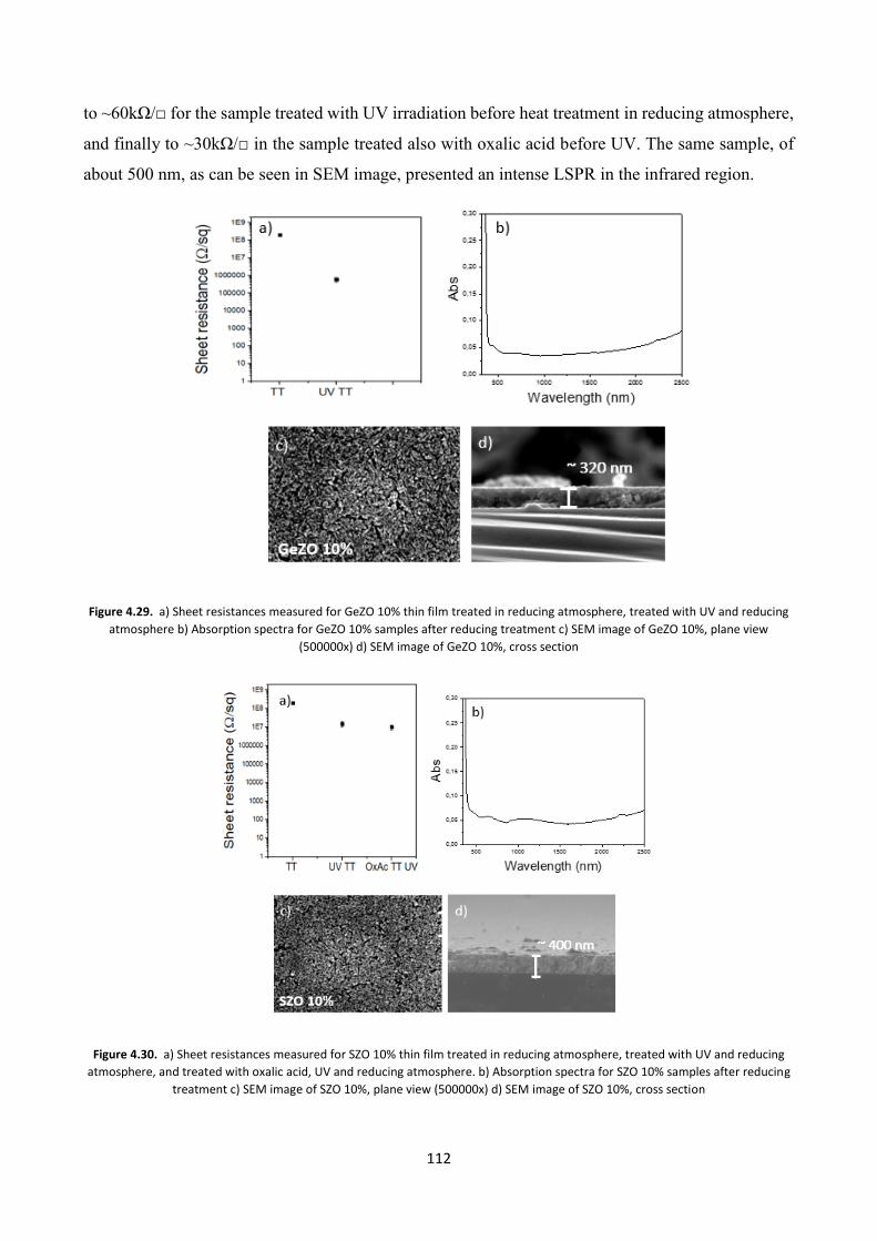
112
to ~60kΩ/□ for the sample treated with UV irradiation before heat treatment in reducing atmosphere,
and finally to ~30kΩ/□ in the sample treated also with oxalic acid before UV. The same sample, of
about 500 nm, as can be seen in SEM image, presented an intense LSPR in the infrared region.
Figure 4.29. a) Sheet resistances measured for GeZO 10% thin film treated in reducing atmosphere, treated with UV and reducing
atmosphere b) Absorption spectra for GeZO 10% samples after reducing treatment c) SEM image of GeZO 10%, plane view
(500000x) d) SEM image of GeZO 10%, cross section
Figure 4.30. a) Sheet resistances measured for SZO 10% thin film treated in reducing atmosphere, treated with UV and reducing
atmosphere, and treated with oxalic acid, UV and reducing atmosphere. b) Absorption spectra for SZO 10% samples after reducing
treatment c) SEM image of SZO 10%, plane view (500000x) d) SEM image of SZO 10%, cross section
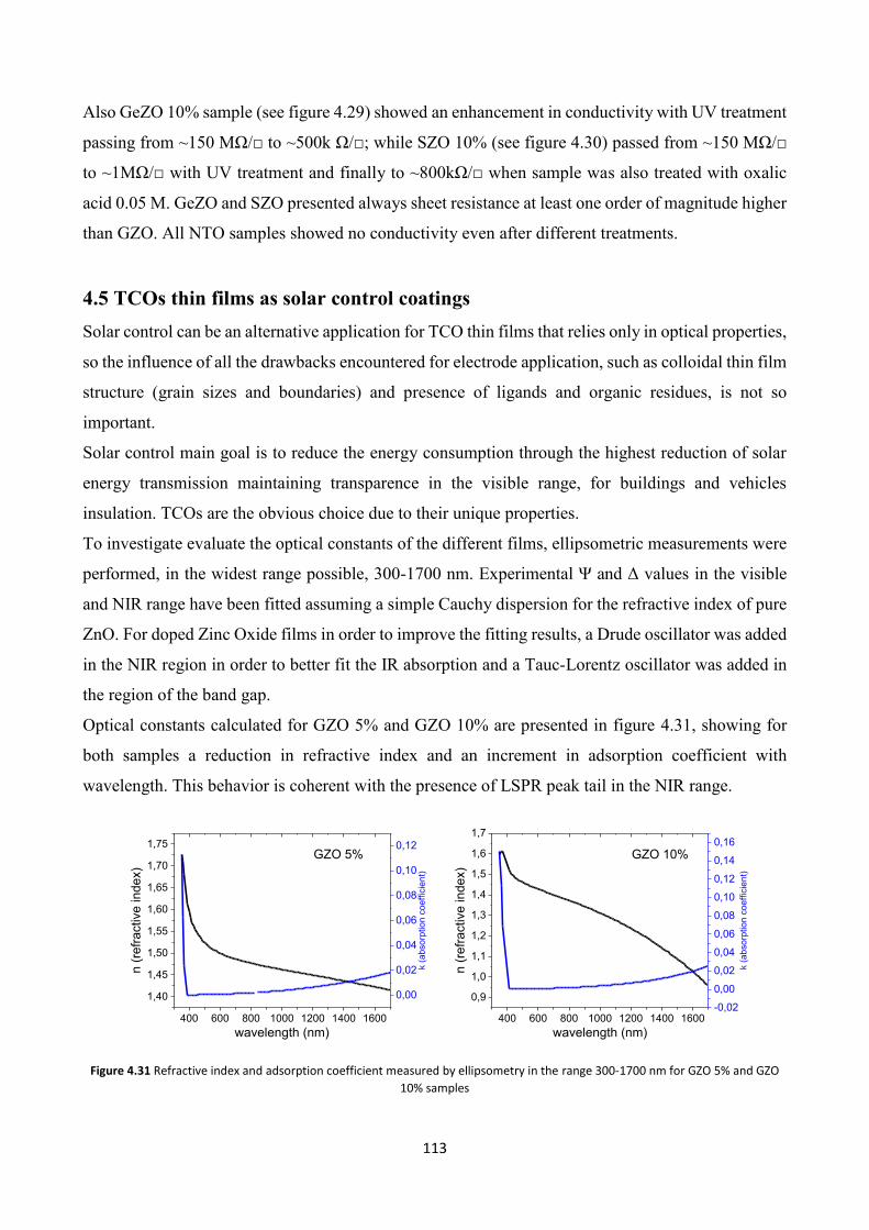
113
Also GeZO 10% sample (see figure 4.29) showed an enhancement in conductivity with UV treatment
passing from ~150 MΩ/□ to ~500k Ω/□; while SZO 10% (see figure 4.30) passed from ~150 MΩ/□
to ~1MΩ/□ with UV treatment and finally to ~800kΩ/□ when sample was also treated with oxalic
acid 0.05 M. GeZO and SZO presented always sheet resistance at least one order of magnitude higher
than GZO. All NTO samples showed no conductivity even after different treatments.
4.5 TCOs thin films as solar control coatings
Solar control can be an alternative application for TCO thin films that relies only in optical properties,
so the influence of all the drawbacks encountered for electrode application, such as colloidal thin film
structure (grain sizes and boundaries) and presence of ligands and organic residues, is not so
important.
Solar control main goal is to reduce the energy consumption through the highest reduction of solar
energy transmission maintaining transparence in the visible range, for buildings and vehicles
insulation. TCOs are the obvious choice due to their unique properties.
To investigate evaluate the optical constants of the different films, ellipsometric measurements were
performed, in the widest range possible, 300-1700 nm. Experimental Ψ and Δ values in the visible
and NIR range have been fitted assuming a simple Cauchy dispersion for the refractive index of pure
ZnO. For doped Zinc Oxide films in order to improve the fitting results, a Drude oscillator was added
in the NIR region in order to better fit the IR absorption and a Tauc-Lorentz oscillator was added in
the region of the band gap.
Optical constants calculated for GZO 5% and GZO 10% are presented in figure 4.31, showing for
both samples a reduction in refractive index and an increment in adsorption coefficient with
wavelength. This behavior is coherent with the presence of LSPR peak tail in the NIR range.
400 600 800 1000 1200 1400 1600
1,40
1,45
1,50
1,55
1,60
1,65
1,70
1,75
wavelength (nm)
n (
refr
active
in
de
x)
0,00
0,02
0,04
0,06
0,08
0,10
0,12
k (
ab
sorp
tio
n c
oeff
icie
nt)
GZO 5%
400 600 800 1000 1200 1400 1600
0,9
1,0
1,1
1,2
1,3
1,4
1,5
1,6
1,7
wavelength (nm)
n (
refr
active
in
de
x)
-0,02
0,00
0,02
0,04
0,06
0,08
0,10
0,12
0,14
0,16
k (
ab
sorp
tio
n c
oeff
icie
nt)
GZO 10%
Figure 4.31 Refractive index and adsorption coefficient measured by ellipsometry in the range 300-1700 nm for GZO 5% and GZO
10% samples

114
Starting from the obtained n and k values, simulations were carried out in a wide spectral range in
order to obtain information on the reflectivity properties of these films even at longer wavelengths.
In fact for solar control application it is important to obtain high reflectivity in the IR region where
the LSPR peaks is centered [3]. In this range it is difficult to perform reflection measurement on thin
films, so we decided to obtain some information on our films behavior through simulations. Moreover
it is possible to simulate reflection spectra for different angles (we choose 0°) and film thickness.
Figures 4.32 and 4.33 show reflection simulation for GZO 5% and GZO 10% for 100 nm, 1000nm,
and the effective thickness of film, 520 nm for GZO 5% and 682 nm for GZO 10%.
2000 4000 6000 8000 10000
0,00
0,05
0,10
0,15
0,20
0,25 1000 nm
520 nm
Re
fle
ctio
n
Wavelength (nm)
100 nm
GZO 5%
Figure 4.32. Reflection simulated using ellispometer software VWase32 for range 300-10000 nm using optical constants gained by
experimental ellipsometry data of GZO 5% sample. Simulated thickness of 100, 520 and 1000 nm.
2000 4000 6000 8000 10000
0,0
0,2
0,4
0,6
0,8
1,0 1000 nm
682 nm
Re
fle
ctio
n
Wavelength (nm)
100 nm
GZO 10%
Figure 4.33. Reflection simulated using ellispometer software VWase32 for range 300-10000 nm using optical constants gained by
experimental ellipsometry data of GZO 10% sample. Simulated thickness of 100, 682 and 1000 nm.

115
Both films presented the same trend, with absolute reflection increasing with thickness. It is
interesting to notice that GZO 10% show very high level of reflection for 682 and 1000 nm of film
thickness, reaching almost 0.9 of reflection at 4000 nm.
In figure 4.34, optical constant for AZO 5%, AZO 10% and AZO 20% samples are presented,
showing similar behavior for AZO 5% and AZO 20%, with k increasing with wavelength, while AZO
10% presented an almost constant value for k.
400 600 800 1000 1200 1400 16001,35
1,40
1,45
1,50
1,55
1,60
wavelength (nm)
n (
refr
active
in
de
x)
0,00
0,05
0,10
0,15
0,20
0,25
k (
absorp
tion c
oeffic
ient)
AZO 5%
400 600 800 1000 1200 1400 1600
1,2
1,3
1,4
1,5
1,6
1,7
wavelength (nm)
n (
refr
active index)
0,0
0,1
0,2
0,3
0,4
0,5
k (
ab
sorp
tio
n c
oeff
icie
nt)
AZO 10%
400 600 800 1000 1200 1400 1600
1,44
1,46
1,48
1,50
1,52
1,54
1,56
1,58
wavelength (nm)
n (
refr
active
in
de
x)
0,00
0,02
0,04
0,06
0,08
0,10
0,12
k (
absorp
tion c
oeffic
ient)
AZO 20%
Figure 4.34 Refractive index and adsorption coefficient measured by ellipsometry in the range 300-1700 nm for AZO 5%, AZO 10%
and AZO 20% samples
2000 4000 6000 8000 10000
0,02
0,03
0,04
0,05
0,06
0,07
0,08
0,09
0,10 1000 nm
340 nm
Re
fle
ctio
n
Wavelength (nm)
100 nm
AZO 5%
Figure 4.35. Reflection simulated using ellispometer software VWase32 for range 300-10000 nm using optical constants gained by
experimental ellipsometry data of AZO 5% sample. Simulated thickness of 100, 340 and 1000 nm.

116
2000 4000 6000 8000 10000
0,0
0,1
0,2
0,3
0,4
0,51000 nm
338 nm
Re
flectio
n
Wavelength (nm)
100 nm
AZO 10%
Figure 4.36. Reflection simulated using ellispometer software VWase32 for range 300-10000 nm using optical constants gained by
experimental ellipsometry data of AZO 10% sample. Simulated thickness of 100, 338 and 1000 nm.
2000 4000 6000 8000 100000,025
0,030
0,035
0,040
0,045
0,050
0,055 1000 nm
300 nm
Reflection
Wavelength (nm)
100 nm
AZO 20%
Figure 4.37. Reflection simulated using ellispometer software VWase32 for range 300-10000 nm using optical constants gained by
experimental ellipsometry data of AZO 20% sample. Simulated thickness of 100, 300 and 1000 nm.
Also for these samples reflection simulations are presented in figure 4.35, 4.36 and 4.37, for 100 nm,
1000 nm and real thickness.
Next samples considered are GeZO 5%, GeZO 10% and GeZO 20%, in figure 4.38 are presented
optical constants versus wavelength, and in figure 4.39, 4.40 and 4.41 the simulations of reflection
for these samples, with thickness of 140, 220 and 240 nm respectively. Also in this case, optical
constant of GeZO lead to a strong reflection in the near infrared region in the simulation.

117
400 600 800 1000 1200 1400 1600
1,46
1,48
1,50
1,52
1,54
1,56
1,58
1,60
1,62
1,64
1,66
wavelength (nm)
n (
refr
active
in
de
x)
0,00
0,02
0,04
0,06
0,08
0,10
0,12
0,14
k (
ab
sorp
tio
n c
oeffic
ient)
GeZO 5%
400 600 800 1000 1200 1400 1600
1,40
1,45
1,50
1,55
1,60
1,65
1,70
wavelength (nm)
n (
refr
active index)
0,00
0,05
0,10
0,15
0,20
0,25
0,30
0,35
0,40
k (
ab
sorp
tio
n c
oeff
icie
nt)
GeZO 10%
400 600 800 1000 1200 1400 1600
1,40
1,42
1,44
1,46
1,48
1,50
1,52
1,54
1,56
wavelength (nm)
n (
refr
active index)
0,00
0,02
0,04
0,06
0,08
0,10
0,12
0,14
0,16
k (
absorp
tion c
oeffic
ient)
GeZO 20%
Figure 4.38. Refractive index and adsorption coefficient measured by ellipsometry in the range 300-1700 nm for GeZO 5%, GeZO
10% and GeZO 20% samples
2000 4000 6000 8000 100000,02
0,03
0,04
0,05
0,06
0,07
0,08
0,09
1000 nm
Re
fle
ctio
n
Wavelength (nm)
140 nm
GeZO 5%
Figure 4.39. Reflection simulated using ellispometer software VWase32 for range 300-10000 nm using optical constants gained by
experimental ellipsometry data of GeZO 5% sample. Simulated thickness of 140 and 1000 nm.

118
2000 4000 6000 8000 100000,02
0,03
0,04
0,05
0,06
0,07
1000 nm
Re
fle
ctio
n
Wavelength (nm)
220 nm
GeZO 10%
Figure 4.40. Reflection simulated using ellispometer software VWase32 for range 300-10000 nm using optical constants gained by
experimental ellipsometry data of GeZO 10% sample. Simulated thickness of 220 and 1000 nm.
2000 4000 6000 8000 10000
0,02
0,03
0,04
0,05
0,06
0,07
1000 nm
Reflection
Wavelength (nm)
240 nm
GeZO 20%
Figure 4.41. Reflection simulated using ellispometer software VWase32 for range 300-10000 nm using optical constants gained by
experimental ellipsometry data of GeZO 20% sample. Simulated thickness of 240 and 1000 nm.
4.6 Conclusions
TCOs thin films were produced via spin coating by high concentrated suspension of colloidal
nanoparticles produced via heat up synthesis. Thin films were then treated with a standard procedure,
consisting in a heat treatment in reducing atmosphere in order to obtain desiderate properties. GZO,
AZO, SZO, GeZO and NTO thin films were characterized through different technique, to study the
effect of dopant concentration on film properties. Some films were then treated through different
approaches, in particular through UV irradiation and organic acids attacks, in order to enhance
electrical conductivity and overcome some limitation of this approach. Finally, thin films optical
constants were used to simulate reflection in the infrared, a key propriety for solar control coatings.
119
References [1] Washo, B.D., Rheology and Modeling of the Spin Coating Process, IBM Journal of Research and
Development, 1977, Volume 21, Issue 2
[2] Enrico Della Gaspera, Marco Bersani, Michela Cittadini, Massimo Guglielmi, Diego Pagani,
Rodrigo Noriega, Saahil Mehra, Alberto Salleo, Alessandro Martucci, Low-Temperature Processed
Ga-Doped ZnO Coatings from Colloidal Inks, J. Am. Chem. Soc. 2013, Volume 135, 3439−3448
[3] Robert M. Pasquarelli, David S. Ginley and Ryan O’Hayre, Solution processing of transparent
conductors: from flask to film Chem. Soc. Rev., 2011, 40, 5406–5441
[4] Joachim Müllera, Bernd Recha, Jiri Springerb, Milan Vanecekb, TCO and light trapping in silicon
thin film solar cells, Solar Energy Volume 77, Issue 6, 2004, Pages 917–930
[5] Hyun Jun Lee, Ju Hyun Hwang, Kyung Bok Choi, Sun-Gyu Jung, Kyu Nyun Kim, Yong Sub Shim,
Cheol Hwee Park, Young Wook Park, and Byeong-Kwon Ju, Effective Indium-Doped Zinc Oxide Buffer
Layer on Silver Nanowires for Electrically Highly Stable, Flexible, Transparent, and Conductive
Composite Electrodes, ACS Appl. Mater. Interfaces 2013, 5, 10397−10403
[6] Areum Kim , Yulim Won , Kyoohee Woo , Sunho Jeong , and Jooho Moon, All-Solution-Processed
Indium-Free Transparent Composite Electrodes based on Ag Nanowire and Metal Oxide for Thin-
Film Solar Cells, Adv. Funct. Mater. 2014, 24, 2462–2471
[7] Hua Tong, Shuxin Ouyang, Yingpu Bi, Naoto Umezawa, Mitsutake Oshikiri, and Jinhua Ye, Nano-
photocatalytic Materials: Possibilities and Challenges, Adv. Mater. 2012, 24, 229–251
[8] Di Claus F. Klingshirn, Andreas Waag, Axel Hoffmann, Jean Geurts, Zinc Oxide: From Fundamental
Properties Towards Novel Applications, 2010
[9] Mohammad H. Zarghami, Yao Liu, Markelle Gibbs, Eminet Gebremichael, Christopher Webster,
and Matt Law, p-Type PbSe and PbS Quantum Dot Solids Prepared with Short-Chain Acids and
Diacids, Acs Nano, 2010, Vol 4, num 2, 2475–2485

120
Chapter 5
Gas Sensing properties of TCO films
5.1 Gas Sensors overview
Nowadays dangerous gases detection is a challenging task, first of all in the safety of working and
living environments: in fact, toxic gases like CO or volatile organic compounds like formaldehyde
can be found easily in those places, carbon monoxide resulting from combustion in shortage of
oxygen and VOC coming from indoor furniture, because they are commonly released from coatings
and adhesives. Sensors can be also used in air monitoring applications, inside buildings or cars, where
the target gas may not be so hazardous or toxic, but its detection and elimination from the environment
can improve the air quality.
These devices have to be characterized by high sensitivity and possibly selectivity. Ideal sensors have
also to be as little as possible, chemically and thermally stable, cheap and long-lasting. Of course a
sensor with all these requirement does not exist nowadays, and maybe it never will: so a compromise
depending on the application is required. For example to check the exhaust gases of a nuclear plant
the cost of the sensor and its working life are obviously less important compared to its accuracy in
determining one particular gas and its absolute concentration; moreover the response has to be as fast
as possible.
A sensor can be defined as a device able to convert a target chemical or physical variation to be
monitored into an easily processable signal; the sensing element has to fulfill essentially two different
tasks: first, it has to interact with the target gas through various mechanisms like surface adsorption,
charge transfer, ionic exchange (receptor task); then this interaction has to be transformed into an
easily processable signal, like for example a change in electrical conductivity or in optical
transmission (transducer task). Different sensors can detect gases through the variation of an optical
property (absorption, reflection, luminescence, refractive index) or electrical property (conductivity,
impedance, capacitance) or other physical properties.
Historically the birth of conductometric sensor is dated 1962, when SnO2 has been used as material
for gas detection [1]: the material resistivity variation was measured changing the surrounding
atmosphere, finding a correlation with the target gas concentration.

121
The main problem of a similar sensor device was the low selectivity, in fact all the gases with similar
chemical-physical behavior will produce similar electrical variation. A solution can be a combination
of different type of sensors connected together. Using different materials and different type of
transducing signals (electrical, thermal, optical, acoustic etc.) permit to obtain the improvement of
the device selectivity [2]. Optical sensors have attracted a lot of interest in the last decades since they
allow to widen the range of operative parameters compared to electrical sensors: in fact variation in
intensity, frequency, polarization and phase of the transmitted/reflected light can be analyzed, and
this can in principle improve the device performances by lowering the cross sensitivity between
different gases. Moreover optical sensors have high temperature, corrosion and fire resistance, they
are electromagnetic noise independent, they don’t require contact measurements; eventually they can
be implemented in optical fiber devices allowing fast and easy signal transport and in situ
measurements with a compact, flexible and environmental robust setup.
Optical sensors can be roughly divided into three main groups: absorbance-based, luminescence-
based and SPR-based, according to the different principles of gas detection. The absorbance-based
sensors employ variation in optical absorption, transmission or reflection after the interaction of the
light with the active materials in the presence of a target molecule. In the luminescence-based sensors,
the photo-luminescence or chemo-luminescence properties of the sensing material are monitored and
related to the target gas concentration: the setup is the basically the same of absorbance-based sensors,
with the exception of the photoluminescence based devices, that require the presence of an excitation
source to promote the luminescence properties of the material.
Speaking about SPR-based sensors, materials that possess a negative real and a small positive
imaginary dielectric constant (like metals) are capable of supporting a SPR. This resonance is a
coherent oscillation of the surface conduction electrons excited by an electromagnetic radiation.
When a surface plasmon is confined to a structure of a size comparable to the wavelength of the
incoming light (for example like in the case of Au or Ag nanoparticles), metal’s free electrons
participate in the collective oscillation, and a localized surface plasmon resonance (LSPR) is excited.
The excitation of the localized surface plasmon results in a strong light scattering, in the appearance
of an intense localized surface plasmon absorption bands and in the enhancement of the local
electromagnetic fields. The frequency and intensity of the LSPR peak highly depends on the geometry
and distribution of the metallic nanostructures, and on the properties of the dielectric surrounding
them.
The LSPR peak of Au and Ag NPs is sensitive to both dielectric constant changes in the supporting
matrix and to changes in electron density of the metal NPs and both these effects have been exploited
for gas sensing applications, like visible in figure 5.1.
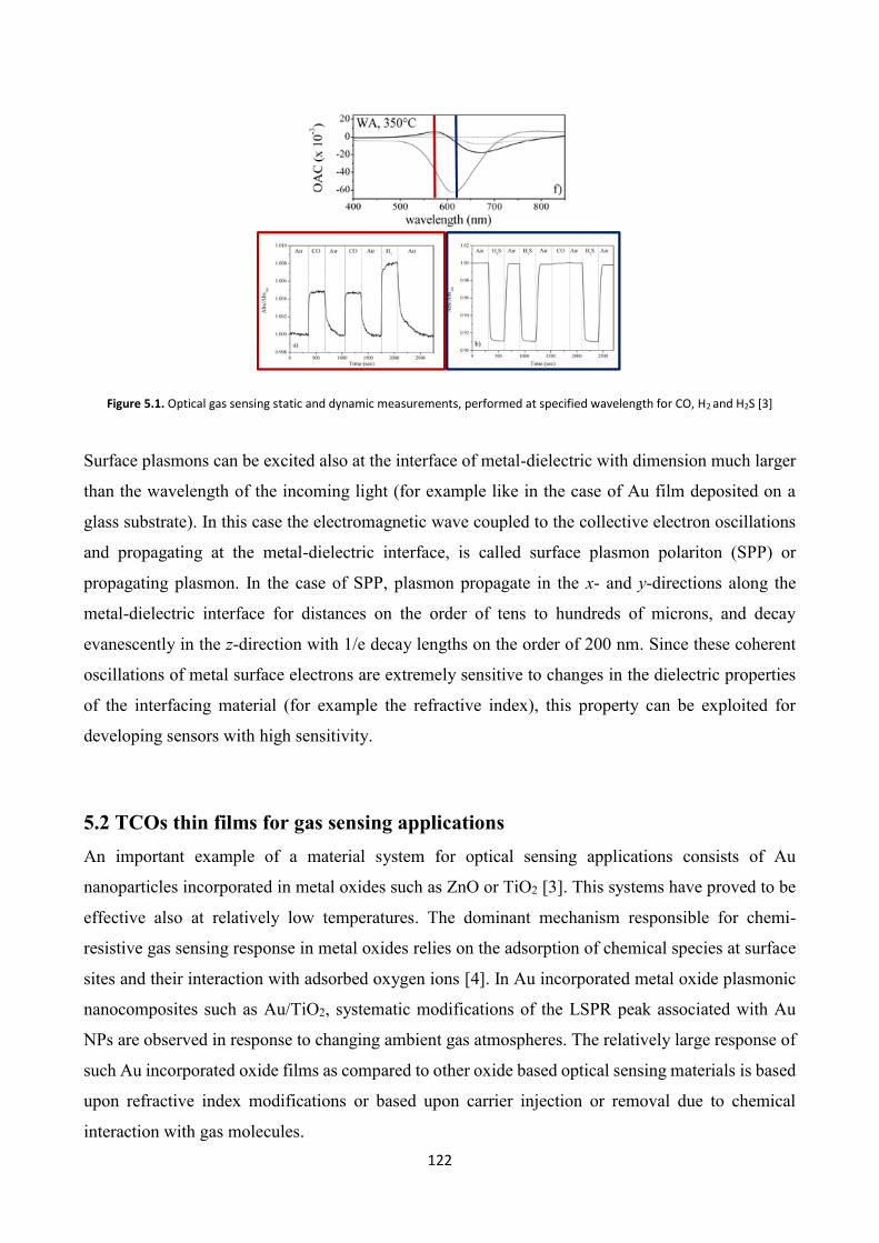
122
Figure 5.1. Optical gas sensing static and dynamic measurements, performed at specified wavelength for CO, H2 and H2S [3]
Surface plasmons can be excited also at the interface of metal-dielectric with dimension much larger
than the wavelength of the incoming light (for example like in the case of Au film deposited on a
glass substrate). In this case the electromagnetic wave coupled to the collective electron oscillations
and propagating at the metal-dielectric interface, is called surface plasmon polariton (SPP) or
propagating plasmon. In the case of SPP, plasmon propagate in the x- and y-directions along the
metal-dielectric interface for distances on the order of tens to hundreds of microns, and decay
evanescently in the z-direction with 1/e decay lengths on the order of 200 nm. Since these coherent
oscillations of metal surface electrons are extremely sensitive to changes in the dielectric properties
of the interfacing material (for example the refractive index), this property can be exploited for
developing sensors with high sensitivity.
5.2 TCOs thin films for gas sensing applications
An important example of a material system for optical sensing applications consists of Au
nanoparticles incorporated in metal oxides such as ZnO or TiO2 [3]. This systems have proved to be
effective also at relatively low temperatures. The dominant mechanism responsible for chemi-
resistive gas sensing response in metal oxides relies on the adsorption of chemical species at surface
sites and their interaction with adsorbed oxygen ions [4]. In Au incorporated metal oxide plasmonic
nanocomposites such as Au/TiO2, systematic modifications of the LSPR peak associated with Au
NPs are observed in response to changing ambient gas atmospheres. The relatively large response of
such Au incorporated oxide films as compared to other oxide based optical sensing materials is based
upon refractive index modifications or based upon carrier injection or removal due to chemical
interaction with gas molecules.
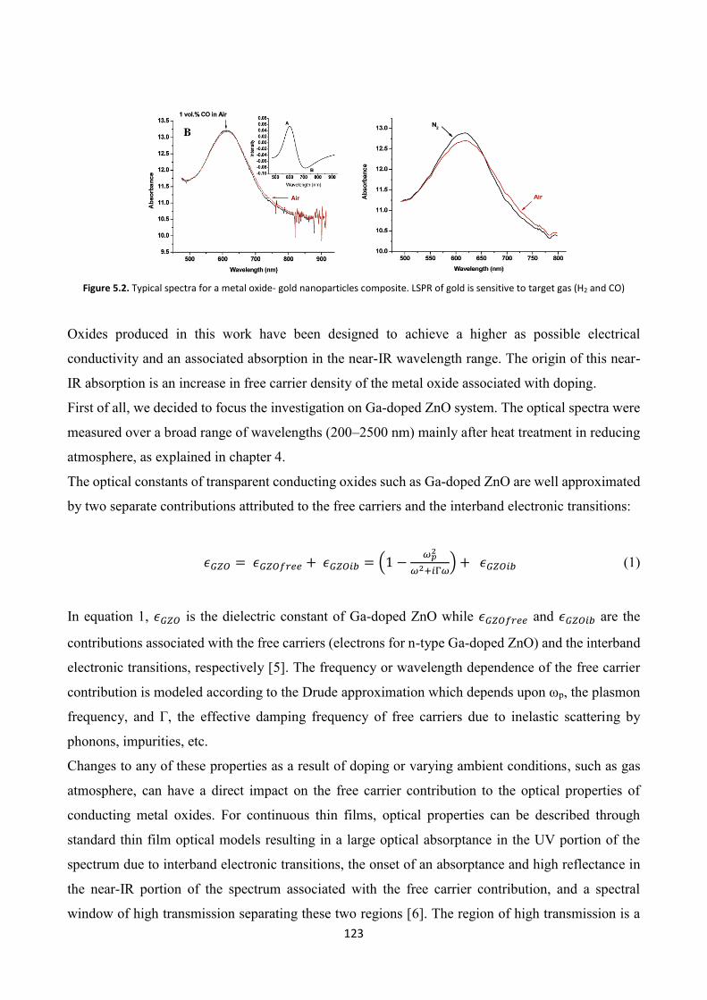
123
Figure 5.2. Typical spectra for a metal oxide- gold nanoparticles composite. LSPR of gold is sensitive to target gas (H2 and CO)
Oxides produced in this work have been designed to achieve a higher as possible electrical
conductivity and an associated absorption in the near-IR wavelength range. The origin of this near-
IR absorption is an increase in free carrier density of the metal oxide associated with doping.
First of all, we decided to focus the investigation on Ga-doped ZnO system. The optical spectra were
measured over a broad range of wavelengths (200–2500 nm) mainly after heat treatment in reducing
atmosphere, as explained in chapter 4.
The optical constants of transparent conducting oxides such as Ga-doped ZnO are well approximated
by two separate contributions attributed to the free carriers and the interband electronic transitions:
𝜖𝐺𝑍𝑂 = 𝜖𝐺𝑍𝑂𝑓𝑟𝑒𝑒 + 𝜖𝐺𝑍𝑂𝑖𝑏 = (1 −𝜔𝑝2
𝜔2+𝑖Γ𝜔) + 𝜖𝐺𝑍𝑂𝑖𝑏 (1)
In equation 1, 𝜖𝐺𝑍𝑂 is the dielectric constant of Ga-doped ZnO while 𝜖𝐺𝑍𝑂𝑓𝑟𝑒𝑒 and 𝜖𝐺𝑍𝑂𝑖𝑏 are the
contributions associated with the free carriers (electrons for n-type Ga-doped ZnO) and the interband
electronic transitions, respectively [5]. The frequency or wavelength dependence of the free carrier
contribution is modeled according to the Drude approximation which depends upon ωp, the plasmon
frequency, and Γ, the effective damping frequency of free carriers due to inelastic scattering by
phonons, impurities, etc.
Changes to any of these properties as a result of doping or varying ambient conditions, such as gas
atmosphere, can have a direct impact on the free carrier contribution to the optical properties of
conducting metal oxides. For continuous thin films, optical properties can be described through
standard thin film optical models resulting in a large optical absorptance in the UV portion of the
spectrum due to interband electronic transitions, the onset of an absorptance and high reflectance in
the near-IR portion of the spectrum associated with the free carrier contribution, and a spectral
window of high transmission separating these two regions [6]. The region of high transmission is a
124
direct consequence of a large bandgap and a relatively low density of free carriers (and hence low ωp)
of the conducting oxides such as GZO (N ~ 1020–1021 cm-3) as compared to free electron metals such
as Ag (N ~ 5.76 × 1022 cm-3).
The noble metals Au and Ag exhibit a strong and pronounced LSPR in the visible region of the
spectrum and hence they are the two most common materials where such effects are investigated and
exploited for similar applications. Recent work has demonstrated that transparent conducting metal
oxides can also exhibit a LSPR peak in the near-IR portion of the spectrum due to the much lower
effective free carrier densities as compared to metals such as Ag and Au.
The lower effective carrier density of GZO as compared to noble metals such as Ag or Au results in
an LSPR absorption peak for GZO nanoparticles in the near-IR portion of the spectrum and only a
short wavelength tail of the absorption peak can be resolved in the full spectral range investigated
experimentally in subsequent sections (i.e. up to 2500 nm).
For noble metal incorporated in metal oxide materials used for plasmonic gas sensing, such as
Au/ZnO and Au/TiO2, a modification of the Au LSPR peak is observed upon changing gas
atmospheres.
The shift and broadening of the peak have been discussed in terms of several potential physical
mechanisms that may be dominant including a change in (1) the free electron density of Au
nanoparticles, (2) the effective dielectric constant of the surrounding matrix (εm), and (3) the damping
frequency of free carriers (Γ) in response to a change in ambient atmospheric conditions . All three
mechanisms have been proposed in the literature depending on the particular material system under
investigation and the temperature at which the sensing experiment was performed. However, noble
metals are known to exhibit properties that depend very weakly upon changes in atmospheric
conditions and changes in relevant material parameters are thought to be mediated through stronger,
direct interactions between the oxide matrix and the ambient atmosphere which can be transduced
into a measurable optical signal through the LSPR peak of the noble metal NPs. In the case of
Au/ZnO, current literature suggests that electronic charge transfer between the oxide matrix and the
noble metal NPs can be responsible for the measured change in the LSPR peak.
But also metal oxides such as TiO2, ZnO, and SnO2 exhibit small changes in electrical resistance as
a function of temperature and/or in response to changing gas atmospheres. These changes in
resistance are primarily associated with surface effects and modifications to the bulk defect chemical
equilibrium at relatively high temperatures.
Conducting metal oxides, such as Ga-doped ZnO, could show the advantage of intrinsic LSPR
sensitivity without adding other plasmonic structures, having a strong dependence of electrical
resistance and carrier concentration. The changes in effective carrier densities of conducting metal
125
oxide NPs in response to changing ambient gas atmospheres would be expected to translate directly
into a change in measured optical absorption associated with free carriers in the near-IR portion of
the spectrum. As such, this unique class of materials can enable a direct optical transduction of the
chemi-resistive response.
Taking ZnO as introductory example, ZnO and generally metal oxides are used and studied
intensively for sensing application, due to the natively presence of vacancies and defects in the oxides
structure. In particular, ZnO is a n-type semiconductor, i.e. with a predominance of oxygen vacancies:
atmospheric oxygen is tipically adsorbed on these surface defects, leading to a change in metal oxide
electrical and optical properties. It has been demonstrated that the predominant type of adsorbed
oxygen is strictly dependent on temperature: in particular the stable oxygen ions are O2-, O- and O=
for temperature T< 100°C, 150°C < T > 300°C and T > 300°C respectively [7].
Given that OT in this work oscillates between room temperature and 200°C, tipical reactions at the
metal oxide surface will be probably the following:
½O2 + e– (cb) → O– (ads) (2)
O2 + e– (cb) → O2- (ads) (3)
while the chemical interaction whit reducing (tipically H2) or oxydizing gas (NO2) will be:
H2 + O– (ads) → H2O + e– (cb) (4)
2H2 + O2= (ads) → 2H2O + e– (cb) (5)
NO2 → NO + O + e– (cb) → O– (ads) (6)
2NO2 → 2NO + 2O + e– (cb) → O2– (ads) (7)
Accordingly to these reactions, reducing and oxydizing gas interaction lead to an injection or a
removal of electron in conduction band, respectively. Carrier density variations can be optically
related to band gap shift (for n-type semiconductor like ZnO, a blue shift for reducing gas and a red
shift for oxidizing gas) through the Burstein-Moss effect [8].
Their plasmon resonance can be also easily tuned with dopant concentration, heat treatments in
particular atmosphere or tailoring grains size and shape, and consequently can be exploited at
different wavelength for different purposes. In figure 5.3 are presented the two main region of interest
for this sensing applications.
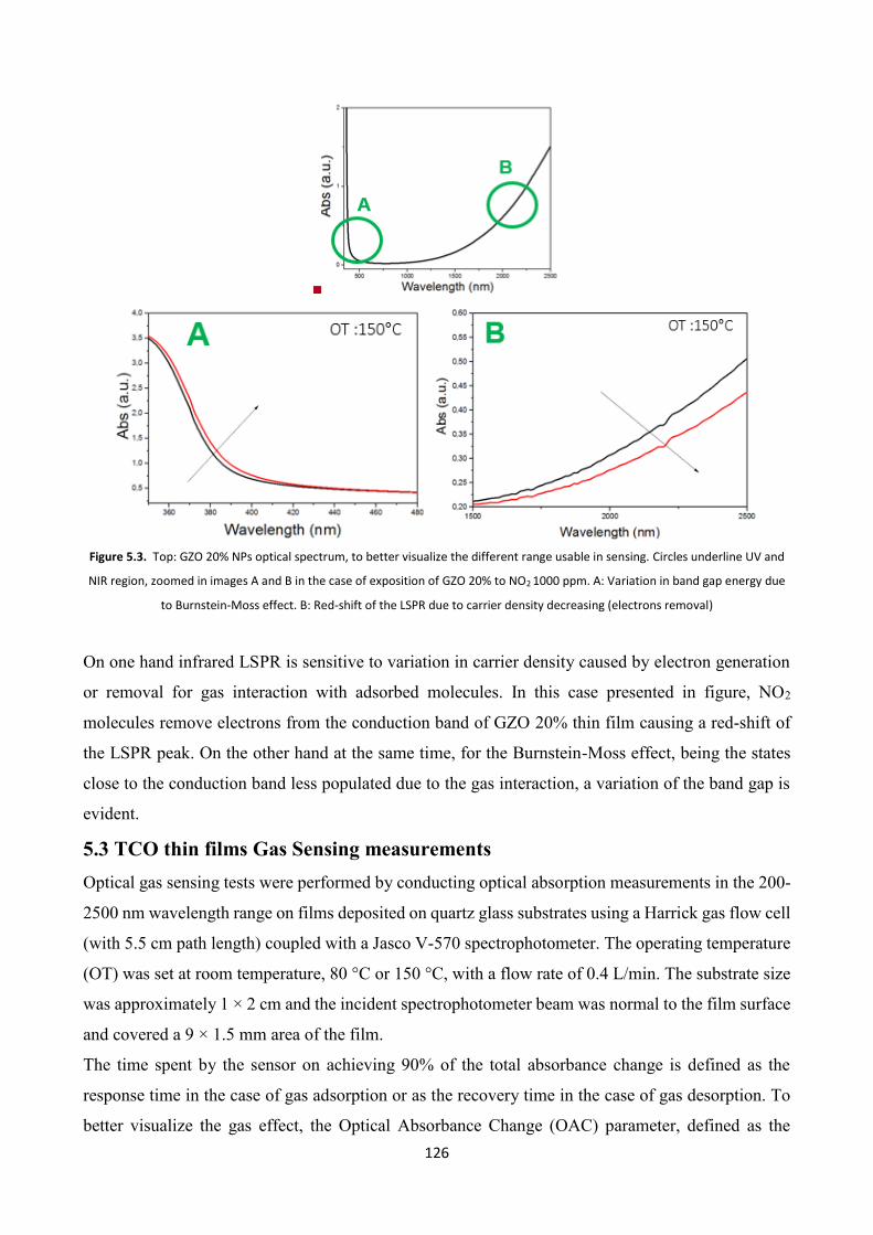
126
Figure 5.3. Top: GZO 20% NPs optical spectrum, to better visualize the different range usable in sensing. Circles underline UV and
NIR region, zoomed in images A and B in the case of exposition of GZO 20% to NO2 1000 ppm. A: Variation in band gap energy due
to Burnstein-Moss effect. B: Red-shift of the LSPR due to carrier density decreasing (electrons removal)
On one hand infrared LSPR is sensitive to variation in carrier density caused by electron generation
or removal for gas interaction with adsorbed molecules. In this case presented in figure, NO2
molecules remove electrons from the conduction band of GZO 20% thin film causing a red-shift of
the LSPR peak. On the other hand at the same time, for the Burnstein-Moss effect, being the states
close to the conduction band less populated due to the gas interaction, a variation of the band gap is
evident.
5.3 TCO thin films Gas Sensing measurements
Optical gas sensing tests were performed by conducting optical absorption measurements in the 200-
2500 nm wavelength range on films deposited on quartz glass substrates using a Harrick gas flow cell
(with 5.5 cm path length) coupled with a Jasco V-570 spectrophotometer. The operating temperature
(OT) was set at room temperature, 80 °C or 150 °C, with a flow rate of 0.4 L/min. The substrate size
was approximately 1 × 2 cm and the incident spectrophotometer beam was normal to the film surface
and covered a 9 × 1.5 mm area of the film.
The time spent by the sensor on achieving 90% of the total absorbance change is defined as the
response time in the case of gas adsorption or as the recovery time in the case of gas desorption. To
better visualize the gas effect, the Optical Absorbance Change (OAC) parameter, defined as the
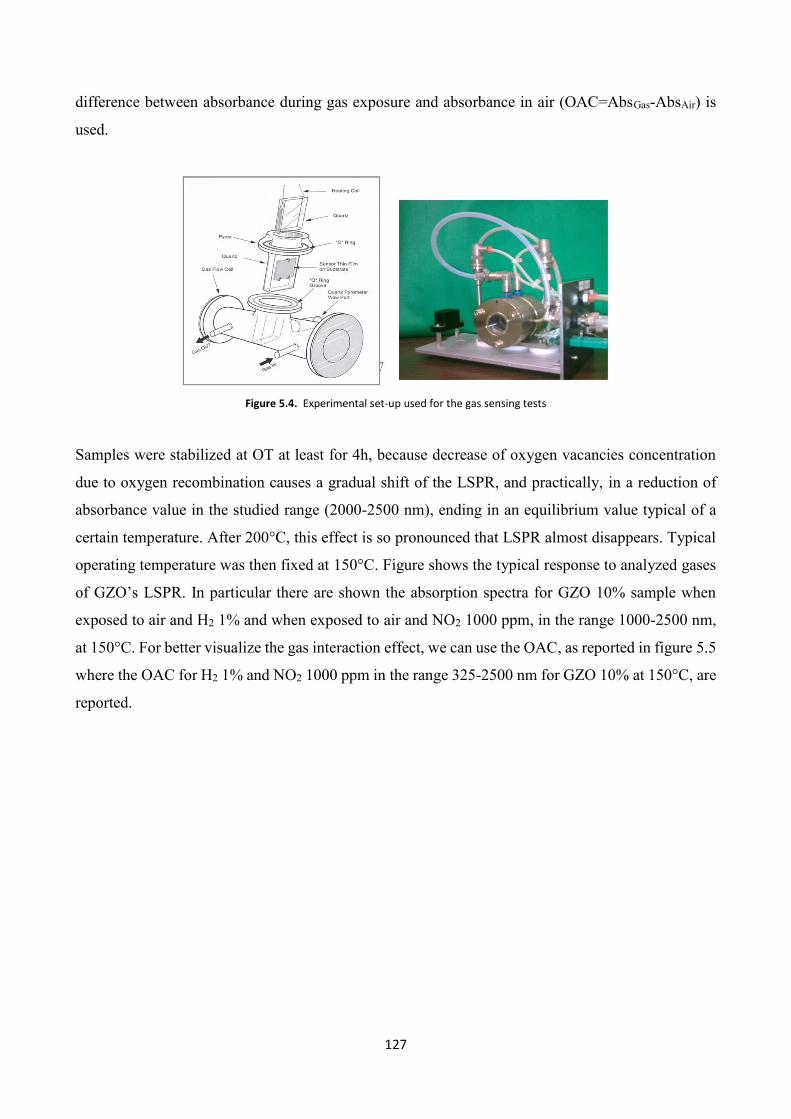
127
difference between absorbance during gas exposure and absorbance in air (OAC=AbsGas-AbsAir) is
used.
Figure 5.4. Experimental set-up used for the gas sensing tests
Samples were stabilized at OT at least for 4h, because decrease of oxygen vacancies concentration
due to oxygen recombination causes a gradual shift of the LSPR, and practically, in a reduction of
absorbance value in the studied range (2000-2500 nm), ending in an equilibrium value typical of a
certain temperature. After 200°C, this effect is so pronounced that LSPR almost disappears. Typical
operating temperature was then fixed at 150°C. Figure shows the typical response to analyzed gases
of GZO’s LSPR. In particular there are shown the absorption spectra for GZO 10% sample when
exposed to air and H2 1% and when exposed to air and NO2 1000 ppm, in the range 1000-2500 nm,
at 150°C. For better visualize the gas interaction effect, we can use the OAC, as reported in figure 5.5
where the OAC for H2 1% and NO2 1000 ppm in the range 325-2500 nm for GZO 10% at 150°C, are
reported.

128
0,2
0,4
b)
Ab
s (
a.u
.)
a)
NO2
1600 2400
0,2
0,4
0,6
Ab
s (
a.u
)
wavelength (nm)
H2
-0,03
0,00
0,03
0,06
c)
OA
C (
Ab
s)
600 1200 1800 2400
-0,1
0,0
0,1
0,2
OA
C (
Ab
s)
d)
wavelength (nm)
Figure 5.5. Optical absorption spectra for GZO 10% sample when exposed to air (black solid lines) and (a) H2 1% vol or (b) NO2 1000
ppm (red dashed lines) at 150°C OT. (c) and (d) show optical absorbance change (OAC = Absgas-Absair) for GZO 10% at 150°C when
exposed to H2 and NO2, respectively.
These behaviours are consistent with NIR plasmonic resonance shifts due to electron density
variations and band gap shifts caused by Burnstein-Moss effect. In the case of hydrogen oxidation,
electrons are injected in the metal oxide, causing a plasmonic blue shift due to increased number of
carriers oscillating and an increase of band gap energy. For oxidizing gases like NO2, gas interaction
with metal oxide causes electrons removal, and a red-shift of plasmon and a decrement in bandgap
energy can be detected. Absolute variation in absorbance is more pronounced in the case of NO2,
rather than H2 at 80°C and 150°C. In the next paragraph the discussion will focus on the comparison
between different TCOs performance to NO2 detection. First of all GZO will be taken as benchmark
oxide, and some consideration about doping effect and temperature effect on optical sensing will be
discussed. Then also other oxides will be considered, and some observation and comparison will be
made. Finally some electrical sensing measurements will be also evaluated, comparing their results
with the optical sensing tests.
Starting with Gallium doped zinc oxide samples, sensitivity to NO2 have been evaluated with the
same procedure for sample containing different amount of dopants. First of all, the sample has been
stabilized in air through a thermal treatment. Then static measurement have been performed: spectra
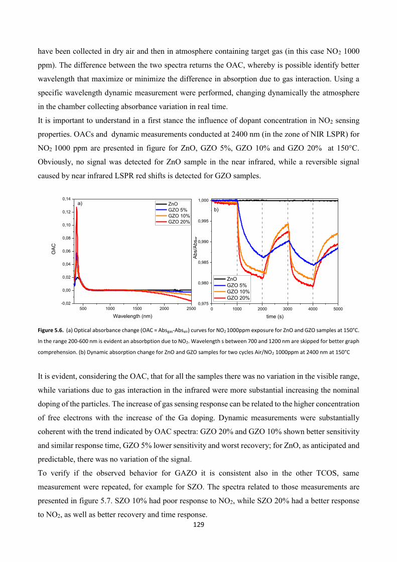
129
have been collected in dry air and then in atmosphere containing target gas (in this case NO2 1000
ppm). The difference between the two spectra returns the OAC, whereby is possible identify better
wavelength that maximize or minimize the difference in absorption due to gas interaction. Using a
specific wavelength dynamic measurement were performed, changing dynamically the atmosphere
in the chamber collecting absorbance variation in real time.
It is important to understand in a first stance the influence of dopant concentration in NO2 sensing
properties. OACs and dynamic measurements conducted at 2400 nm (in the zone of NIR LSPR) for
NO2 1000 ppm are presented in figure for ZnO, GZO 5%, GZO 10% and GZO 20% at 150°C.
Obviously, no signal was detected for ZnO sample in the near infrared, while a reversible signal
caused by near infrared LSPR red shifts is detected for GZO samples.
500 1000 1500 2000 2500
-0,02
0,00
0,02
0,04
0,06
0,08
0,10
0,12
0,14
0 1000 2000 3000 4000 5000
0,975
0,980
0,985
0,990
0,995
1,000
b)
OA
C
Wavelength (nm)
ZnO
GZO 5%
GZO 10%
GZO 20%
a)
Ab
s/A
bs
air
time (s)
ZnO
GZO 5%
GZO 10%
GZO 20%
Figure 5.6. (a) Optical absorbance change (OAC = Absgas-Absair) curves for NO2 1000ppm exposure for ZnO and GZO samples at 150°C.
In the range 200-600 nm is evident an absorbption due to NO2. Wavelength s between 700 and 1200 nm are skipped for better graph
comprehension. (b) Dynamic absorption change for ZnO and GZO samples for two cycles Air/NO2 1000ppm at 2400 nm at 150°C
It is evident, considering the OAC, that for all the samples there was no variation in the visible range,
while variations due to gas interaction in the infrared were more substantial increasing the nominal
doping of the particles. The increase of gas sensing response can be related to the higher concentration
of free electrons with the increase of the Ga doping. Dynamic measurements were substantially
coherent with the trend indicated by OAC spectra: GZO 20% and GZO 10% shown better sensitivity
and similar response time, GZO 5% lower sensitivity and worst recovery; for ZnO, as anticipated and
predictable, there was no variation of the signal.
To verify if the observed behavior for GAZO it is consistent also in the other TCOS, same
measurement were repeated, for example for SZO. The spectra related to those measurements are
presented in figure 5.7. SZO 10% had poor response to NO2, while SZO 20% had a better response
to NO2, as well as better recovery and time response.
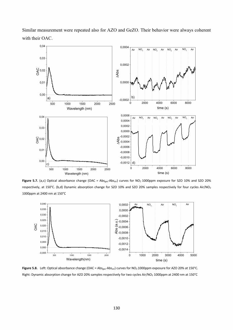
130
Similar measurement were repeated also for AZO and GeZO. Their behavior were always coherent
with their OAC.
500 1000 1500 2000 2500
0,00
0,01
0,02
0,03
0,04
OA
C
Wavelength (nm)
a)
0 2000 4000 6000 8000-0,0002
0,0000
0,0002
0,0004NO
2 NO2
NO2
AirAirAirAirAir NO2
A
bs
time (s)
b)
500 1000 1500 2000 2500
0,00
0,01
0,02
0,03
0,04
OA
C
Wavelength (nm)
c)
0 2000 4000 6000 8000
-0,0012
-0,0010
-0,0008
-0,0006
-0,0004
-0,0002
0,0000
0,0002
0,0004
0,0006NO
2 NO2
NO2
AirAirAirAirAir NO2
Ab
s
time (s)
d)
Figure 5.7. (a,c) Optical absorbance change (OAC = Absgas-Absair) curves for NO2 1000ppm exposure for SZO 10% and SZO 20%
respectively, at 150°C. (b,d) Dynamic absorption change for SZO 10% and SZO 20% samples respectively for four cycles Air/NO2
1000ppm at 2400 nm at 150°C
500 1000 1500 2000
-0,005
0,000
0,005
0,010
0,015
0,020
0,025
0,030
0,035
0,040
OA
C
Wavelength(nm)
0 1000 2000 3000 4000 5000
-0,0014
-0,0012
-0,0010
-0,0008
-0,0006
-0,0004
-0,0002
0,0000
0,0002 AirAirAir NO2
NO2
Abs (
a.u
.)
time (s)
Figure 5.8. Left: Optical absorbance change (OAC = Absgas-Absair) curves for NO2 1000ppm exposure for AZO 20% at 150°C.
Right: Dynamic absorption change for AZO 20% samples respectively for two cycles Air/NO2 1000ppm at 2400 nm at 150°C

131
500 1000 1500 2000 2500-0,02
-0,01
0,00
0,01
0,02
0,03
0,04
0,05
0,06
0,07
OA
C
Wavelength (nm)
GeZO 20%
150°C
NO2 1000 ppm
0 1000 2000 3000 4000 5000
-0,0030
-0,0025
-0,0020
-0,0015
-0,0010
-0,0005
0,0000
0,0005 AirAirAir NO2
NO2
A
bs
time (s)
GeZO 20%150°C
Figure 5.9. Left: Optical absorbance change (OAC = Absgas-Absair) curves for NO2 1000ppm exposure for GeZO 20% at 150°C.
Right: Dynamic absorption change for GeZO 20% sample for two cycles Air/NO2 1000ppm at 2400 nm at 150°C
Figure 5.10. Left: Optical absorbance change (OAC = Absgas-Absair) curves for NO2 1000ppm exposure for GZO 20%, AZO 20%, SZO
20%, GeZO 20% samples at 150°C. Right: Dynamic absorption change GZO 20%, AZO 20%, SZO 20%, GeZO 20% samples for two cycles
Air/NO2 1000ppm at 2400 nm at 150°C
Figure 5.10 summarize the behavior for doped zinc oxides produced at 20% nominal doping. It is
interesting to underline that different response intensity for different oxides (at 2400nm, in the NIR
region) is consistent with both the OAC trend and, more important, with absorbance spectra of the
different oxides, shown in figure 5.11, showing always a n-type response. This effect seems to point
out a direct correlation between the position of the LSPR (that is linked to carrier density) to the
response intensity.
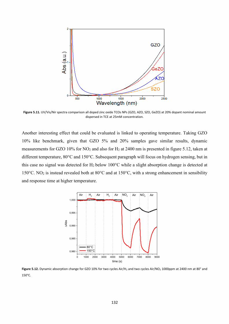
132
Figure 5.11. UV/Vis/Nir spectra comparison all doped zinc oxide TCOs NPs (GZO, AZO, SZO, GeZO) at 20% dopant nominal amount
dispersed in TCE at 25mM concentration.
Another interesting effect that could be evaluated is linked to operating temperature. Taking GZO
10% like benchmark, given that GZO 5% and 20% samples gave similar results, dynamic
measurements for GZO 10% for NO2 and also for H2 at 2400 nm is presented in figure 5.12, taken at
different temperature, 80°C and 150°C. Subsequent paragraph will focus on hydrogen sensing, but in
this case no signal was detected for H2 below 100°C while a slight absorption change is detected at
150°C. NO2 is instead revealed both at 80°C and at 150°C, with a strong enhancement in sensibility
and response time at higher temperature.
0 1000 2000 3000 4000 5000 6000 7000 8000 9000
0,980
0,985
0,990
0,995
1,000
A
bs
time (s)
80°C
150°C
Air H2
Air H2
Air NO2 Air NO
2Air
Figure 5.12. Dynamic absorption change for GZO 10% for two cycles Air/H2 and two cycles Air/NO2 1000ppm at 2400 nm at 80° and
150°C.

133
500 1000 1500 2000 2500-0,010
-0,005
0,000
0,005
0,010
0,015
0,020
0,025
150°C
OA
C
Wavelength (nm)
80°C
0 2000 4000 6000
0,196
0,198
0,200
0,202
0,204
0,206
0,208
0,210
0,212
0,214
0,216NO
2
150°C
Abs (
a.u
.)
time (s)
80°C
NO2
Figure 5.13. Left: Optical absorbance change (OAC = Absgas-Absair) curves for NO2 1000ppm exposure for NTO 20% at 80°C and 150°C.
Right: Dynamic absorption change for NTO 20% for two cycles Air/NO2 1000ppm at 2400 nm at 80° and 150°C.
This effect was evaluated for all the other TCO materials, showing almost similar behavior. In figure
5.13 are presented some results for NTO 20% sample, with OAC curves for NO2 1000 ppm at 80°C
and 150°C and the correlated dynamic measurements taken at 2400 nm. At 80°C signal was quite
noisy, while at 150°C better response intensity, even if little drift was present.
Those temperatures were find to be optimal for almost all the samples because at room temperature
signal appeared to be too noisy, while at higher temperatures the LSPR was shifting, due to oxygen
recombination and carrier density decrease. In fac,t above 200-250°C LSPR tail disappears from the
analyzed range (200-2500 nm).
In addition to what we have seen previously, it is worth focusing on some aspects that could appear
secondary or less important but actually necessary to understand some mechanisms and concepts
behind experiments.
0 2000 4000 6000 8000 10000
2,42
2,44
2,46
2,48
2,50
2,52
2,54
2,56
2,58AirAirAirAirAirAir CO NO
2NO
2H2
Ab
s (
a.u
.)
time (s)
H2
a)
380 nm
150°C
GZO 10% Pt
0 2000 4000 6000 8000 100000,475
0,480
0,485
0,490
0,495
0,500
0,505
0,510
2400 nm
150°C
GZO 10% Pt
AirAirAirAirAir CO NO2NO
2H
2
Ab
s (
a.u
.)
time (s)
H2
b)
Figure 5.14. a) Dynamic absorption variation for GZO 10% with Platinum sample for two cycles Air/H2 1%, one cycle Air/CO 1% and
two cycles Air/NO2 at 380 nm at 150°C b) Dynamic absorption variation for GZO 10% with Platinum sample for two cycles Air/H2
1%, one cycle Air/CO 1% and two cycles Air/NO2 at 2400 nm at 150°C

134
For example for every measurement done in the near infrared range exploiting typical LSPR of TCOs,
it is possible to gain same results in band gap region: in figure 5.14 are presented dynamic
measurements for GZO 10% with Platinum in order to detect H2 1%, NO2 1000 ppm and CO 1%,
performed both at 380 nm (band gap, varying for Burnstein-Moss) and at 2400 nm (shift of LSPR),
showing clear response and good recovery to H2 and NO2, while no signal was detected for CO,
proving selectivity of the sensor. This fact can be useful to obtain other information about the nature
of semiconductor oxide and other different aspects. Thanks to TCOs behavior in these two different
regions, different wavelength can be chosen to perform the dynamic measurements, which will be
used in the final application. Moreover TCOs, leaving free the visible range, let other materials work
in the visible (Au NPs).
GZO samples were then subjected to electrical gas sensing tests in order to have a comparison with
optical gas sensing measurements. Figure 5.15 shows the behavior of ZnO, GZO 10% and GZO 20%
samples for an Air/NO2 400 ppb cycle increasing the operating temperature (OT) from 25 to 75 °C.
Room temperature response is not reported since no response was found at this temperature.
Figure 5.15. Normalized resistance variation for ZnO, GZO 10% and GZO 20% for one cycle Air/NO2 400 ppb at 25° and 75°C.
For all the considered temperatures Gallium doping enhanced the relative response to NO2, in
particular increasing Gallium concentration lead to an increment in relative response, and the
difference in response between GZO 10% and GZO 20% was more pronounced at low temperatures.
These results represent a confirmation of optical sensing measurements.
All the films showed n-type response to NO2 that is an oxidizing gas, causing an increase. The
reaction mechanism of the target gas with the film surface takes into account the fact that ZnO metal
oxide is slightly off-stoichiometric resulting in a deficiency of lattice oxygen. Depending on the OT,
ambient oxygen is known to chemisorb on oxygen vacancies making the resistance to increase. NO2
oxidizing gas adsorbs directly on the ZnO surface following previous reported reactions (6) and (7).
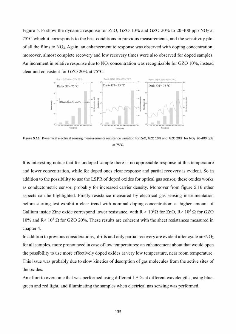
135
Figure 5.16 show the dynamic response for ZnO, GZO 10% and GZO 20% to 20-400 ppb NO2 at
75°C which it corresponds to the best conditions in previous measurements, and the sensitivity plot
of all the films to NO2. Again, an enhancement to response was observed with doping concentration;
moreover, almost complete recovery and low recovery times were also observed for doped samples.
An increment in relative response due to NO2 concentration was recognizable for GZO 10%, instead
clear and consistent for GZO 20% at 75°C.
Figure 5.16. Dynamical electrical sensing measurements resistance variation for ZnO, GZO 10% and GZO 20% for NO2 20-400 ppb
at 75°C.
It is interesting notice that for undoped sample there is no appreciable response at this temperature
and lower concentration, while for doped ones clear response and partial recovery is evident. So in
addition to the possibility to use the LSPR of doped oxides for optical gas sensor, these oxides works
as conductometric sensor, probably for increased carrier density. Moreover from figure 5.16 other
aspects can be highlighted. Firstly resistance measured by electrical gas sensing instrumentation
before starting test exhibit a clear trend with nominal doping concentration: at higher amount of
Gallium inside Zinc oxide correspond lower resistance, with R > 106Ω for ZnO, R> 105 Ω for GZO
10% and R< 105 Ω for GZO 20%. These results are coherent with the sheet resistances measured in
chapter 4.
In addition to previous considerations, drifts and only partial recovery are evident after cycle air/NO2
for all samples, more pronounced in case of low temperatures: an enhancement about that would open
the possibility to use more effectively doped oxides at very low temperature, near room temperature.
This issue was probably due to slow kinetics of desorption of gas molecules from the active sites of
the oxides.
An effort to overcome that was performed using different LEDs at different wavelengths, using blue,
green and red light, and illuminating the samples when electrical gas sensing was performed.
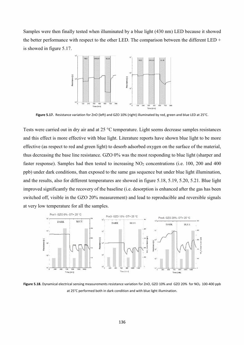
136
Samples were then finally tested when illuminated by a blue light (430 nm) LED because it showed
the better performance with respect to the other LED. The comparison between the different LED +
is showed in figure 5.17.
Figure 5.17. Resistance variation for ZnO (left) and GZO 10% (right) illuminated by red, green and blue LED at 25°C.
Tests were carried out in dry air and at 25 °C temperature. Light seems decrease samples resistances
and this effect is more effective with blue light. Literature reports have shown blue light to be more
effective (as respect to red and green light) to desorb adsorbed oxygen on the surface of the material,
thus decreasing the base line resistance. GZO 0% was the most responding to blue light (sharper and
faster response). Samples had then tested to increasing NO2 concentrations (i.e. 100, 200 and 400
ppb) under dark conditions, than exposed to the same gas sequence but under blue light illumination,
and the results, also for different temperatures are showed in figure 5.18, 5.19, 5.20, 5.21. Blue light
improved significantly the recovery of the baseline (i.e. desorption is enhanced after the gas has been
switched off, visible in the GZO 20% measurement) and lead to reproducible and reversible signals
at very low temperature for all the samples.
Figure 5.18. Dynamical electrical sensing measurements resistance variation for ZnO, GZO 10% and GZO 20% for NO2 100-400 ppb
at 25°C performed both in dark condition and with blue light illumination.

137
Figure 5.19. Dynamical electrical sensing measurements resistance variation for ZnO, GZO 10% and GZO 20% for NO2 20-400 ppb
at 50°C performed both in dark condition and with blue light illumination.
Figure 5.20. Dynamical electrical sensing measurements resistance variation for ZnO, GZO 10% and GZO 20% for NO2 20-400 ppb
at 75°C performed both in dark condition and with blue light illumination.
Figure 5.21. Dynamical electrical sensing measurements resistance variation for ZnO, GZO 10% and GZO 20% for NO2 20-400 ppb
at 100°C performed both in dark condition and with blue light illumination.
At 75°C and 100°C, dynamic measurements showed in figure proved that for every condition all
samples respond to every NO2 concentration used (100-200-400 ppb). These results pointed out some
effects: (1) for every sample, blue illumination involved better performance both in absolute response
and in recovery, due to better kinetics of desorption of molecules bound to oxide surface; (2) this
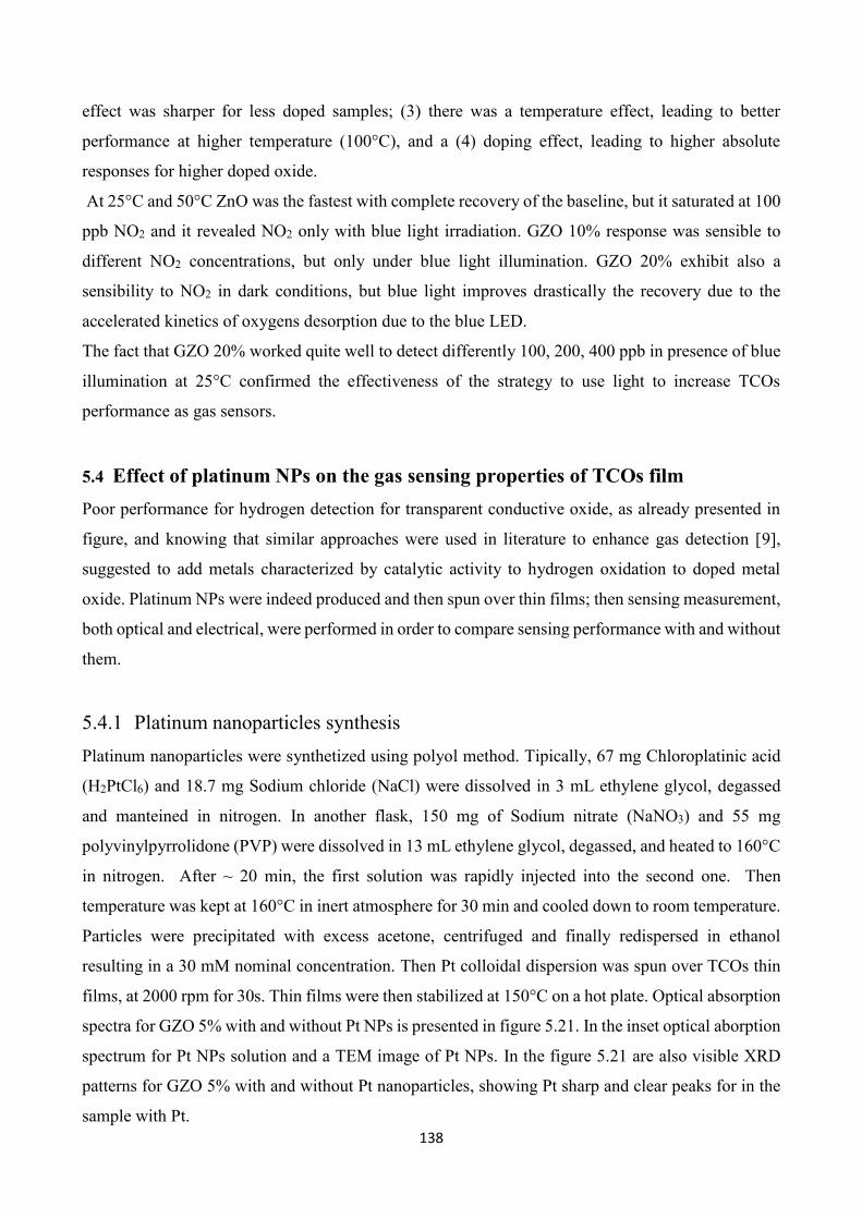
138
effect was sharper for less doped samples; (3) there was a temperature effect, leading to better
performance at higher temperature (100°C), and a (4) doping effect, leading to higher absolute
responses for higher doped oxide.
At 25°C and 50°C ZnO was the fastest with complete recovery of the baseline, but it saturated at 100
ppb NO2 and it revealed NO2 only with blue light irradiation. GZO 10% response was sensible to
different NO2 concentrations, but only under blue light illumination. GZO 20% exhibit also a
sensibility to NO2 in dark conditions, but blue light improves drastically the recovery due to the
accelerated kinetics of oxygens desorption due to the blue LED.
The fact that GZO 20% worked quite well to detect differently 100, 200, 400 ppb in presence of blue
illumination at 25°C confirmed the effectiveness of the strategy to use light to increase TCOs
performance as gas sensors.
5.4 Effect of platinum NPs on the gas sensing properties of TCOs film
Poor performance for hydrogen detection for transparent conductive oxide, as already presented in
figure, and knowing that similar approaches were used in literature to enhance gas detection [9],
suggested to add metals characterized by catalytic activity to hydrogen oxidation to doped metal
oxide. Platinum NPs were indeed produced and then spun over thin films; then sensing measurement,
both optical and electrical, were performed in order to compare sensing performance with and without
them.
5.4.1 Platinum nanoparticles synthesis
Platinum nanoparticles were synthetized using polyol method. Tipically, 67 mg Chloroplatinic acid
(H2PtCl6) and 18.7 mg Sodium chloride (NaCl) were dissolved in 3 mL ethylene glycol, degassed
and manteined in nitrogen. In another flask, 150 mg of Sodium nitrate (NaNO3) and 55 mg
polyvinylpyrrolidone (PVP) were dissolved in 13 mL ethylene glycol, degassed, and heated to 160°C
in nitrogen. After ~ 20 min, the first solution was rapidly injected into the second one. Then
temperature was kept at 160°C in inert atmosphere for 30 min and cooled down to room temperature.
Particles were precipitated with excess acetone, centrifuged and finally redispersed in ethanol
resulting in a 30 mM nominal concentration. Then Pt colloidal dispersion was spun over TCOs thin
films, at 2000 rpm for 30s. Thin films were then stabilized at 150°C on a hot plate. Optical absorption
spectra for GZO 5% with and without Pt NPs is presented in figure 5.21. In the inset optical aborption
spectrum for Pt NPs solution and a TEM image of Pt NPs. In the figure 5.21 are also visible XRD
patterns for GZO 5% with and without Pt nanoparticles, showing Pt sharp and clear peaks for in the
sample with Pt.
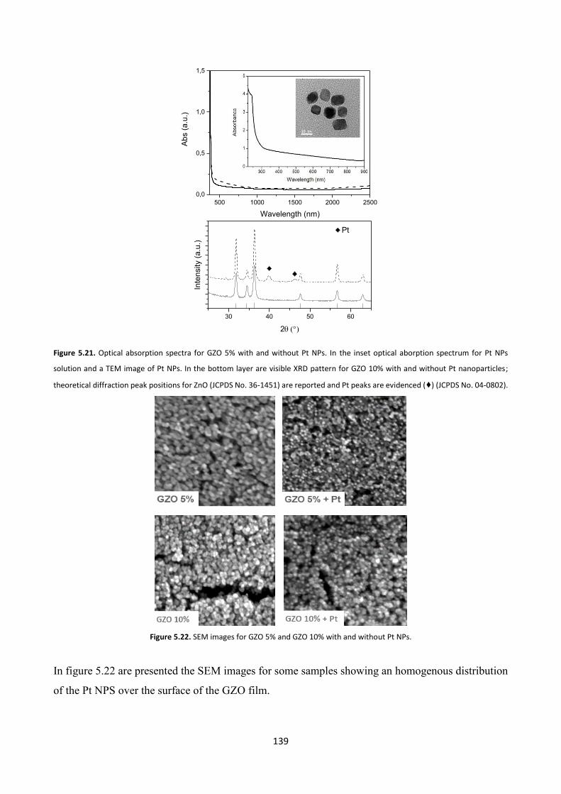
139
500 1000 1500 2000 2500
0,0
0,5
1,0
1,5
Ab
s (
a.u
.)
Wavelength (nm)
30 40 50 60
Inte
nsity (
a.u
.)
2
Pt
Figure 5.21. Optical absorption spectra for GZO 5% with and without Pt NPs. In the inset optical aborption spectrum for Pt NPs
solution and a TEM image of Pt NPs. In the bottom layer are visible XRD pattern for GZO 10% with and without Pt nanoparticles;
theoretical diffraction peak positions for ZnO (JCPDS No. 36-1451) are reported and Pt peaks are evidenced (♦) (JCPDS No. 04-0802).
Figure 5.22. SEM images for GZO 5% and GZO 10% with and without Pt NPs.
In figure 5.22 are presented the SEM images for some samples showing an homogenous distribution
of the Pt NPS over the surface of the GZO film.

140
5.4.2 Gas sensing measurements
Optical gas sensing measurements on GZO thin films with and without Platinum were carried on with
the same variables previously used for sensing tests. First of all simple experiment to verify the
influence of Platinum on hydrogen response was performed.
In figure 5.23 are plotted the dynamic sensing measurements for two cycles Air/H2 for GZO 5% and
GZO 5% with Platinum at 2400 nm at 150°C. A great enhancement in hydrogen sensitivity confirm
the catalytic activity of Platinum in the hydrogen oxidation.
Figure 5.23. Dynamic absorption variation for GZO 5% and GZO 5% with Platinum samples for two cycles Air/H2 1% at 2400 nm at
150°C
0 1000 2000 3000 4000 5000 6000 7000 8000 9000
0,992
0,996
1,000
1,004
GZO Pt 10%
AirAir NO2NO2AirAir H2
Ab
s (
a.u
.)
time (s)
H2Air
2400 nm 150°C
GZO Pt 5%
Figure 5.24. Dynamic absorption variation for GZO 5% with Platinum and GZO 10% with Platinum samples for two cycles Air/H2 1%
and two cycles Air/NO2 at 2400 nm at 150°C
Doping effect in the sample with Platinum, as it has been done in the bare oxides samples, can be
deduced simply the dynamic measurements represented in figure 5.24. GZO 5% with Platinum had a
good response to H2 and also to NO2 at 2400 nm at 150°C, while GZO 10% with Platinum showed
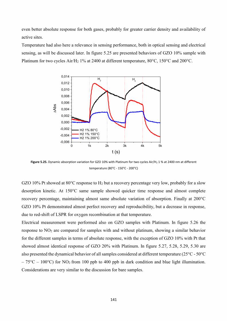
141
even better absolute response for both gases, probably for greater carrier density and availability of
active sites.
Temperature had also here a relevance in sensing performance, both in optical sensing and electrical
sensing, as will be discussed later. In figure 5.25 are presented behaviors of GZO 10% sample with
Platinum for two cycles Air/H2 1% at 2400 at different temperature, 80°C, 150°C and 200°C.
0 1k 2k 3k 4k 5k-0,006
-0,004
-0,002
0,000
0,002
0,004
0,006
0,008
0,010
0,012
0,014H
2
H2 1% 80°C
H2 1% 150°C
H2 1% 200°C
A
bs
t (s)
H2
Figure 5.25. Dynamic absorption variation for GZO 10% with Platinum for two cycles Air/H2 1 % at 2400 nm at different
temperature (80°C - 150°C - 200°C)
GZO 10% Pt showed at 80°C response to H2 but a recovery percentage very low, probably for a slow
desorption kinetic. At 150°C same sample showed quicker time response and almost complete
recovery percentage, maintaining almost same absolute variation of absorption. Finally at 200°C
GZO 10% Pt demonstrated almost perfect recovery and reproducibility, but a decrease in response,
due to red-shift of LSPR for oxygen recombination at that temperature.
Electrical measurement were performed also on GZO samples with Platinum. In figure 5.26 the
response to NO2 are compared for samples with and without platinum, showing a similar behavior
for the different samples in terms of absolute response, with the exception of GZO 10% with Pt that
showed almost identical response of GZO 20% with Platinum. In figure 5.27, 5.28, 5.29, 5.30 are
also presented the dynamical behavior of all samples considered at different temperature (25°C - 50°C
– 75°C – 100°C) for NO2 from 100 ppb to 400 ppb in dark condition and blue light illumination.
Considerations are very similar to the discussion for bare samples.

142
Figure 5.26. Normalized resistance variation for ZnO GZO 10% and GZO 20%, and same samples with Platinum for one cycle
Air/NO2 400 ppb at and 75°C.
Figure 5.27. Dynamical electrical sensing measurements resistance variation for ZnO with Platinum, GZO 10% with Platinum and
GZO 20% with platinum for NO2 100-400 ppb at 25°C performed both in dark condition and with blue light illumination.
Figure 5.28. Dynamical electrical sensing measurements resistance variation for ZnO with Platinum, GZO 10% with Platinum and
GZO 20% with platinum for NO2 100-400 ppb at 50°C performed both in dark condition and with blue light illumination.
Figure 5.29. Dynamical electrical sensing measurements resistance variation for ZnO with Platinum, GZO 10% with Platinum and
GZO 20% with platinum for NO2 100-400 ppb at 75°C performed both in dark condition and with blue light illumination.
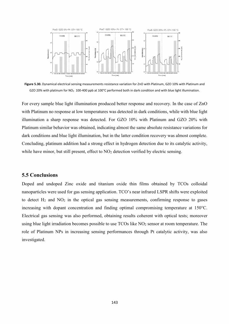
143
Figure 5.30. Dynamical electrical sensing measurements resistance variation for ZnO with Platinum, GZO 10% with Platinum and
GZO 20% with platinum for NO2 100-400 ppb at 100°C performed both in dark condition and with blue light illumination.
For every sample blue light illumination produced better response and recovery. In the case of ZnO
with Platinum no response at low temperatures was detected in dark conditions, while with blue light
illumination a sharp response was detected. For GZO 10% with Platinum and GZO 20% with
Platinum similar behavior was obtained, indicating almost the same absolute resistance variations for
dark conditions and blue light illumination, but in the latter condition recovery was almost complete.
Concluding, platinum addition had a strong effect in hydrogen detection due to its catalytic activity,
while have minor, but still present, effect to NO2 detection verified by electric sensing.
5.5 Conclusions
Doped and undoped Zinc oxide and titanium oxide thin films obtained by TCOs colloidal
nanoparticles were used for gas sensing application. TCO’s near infrared LSPR shifts were exploited
to detect H2 and NO2 in the optical gas sensing measurements, confirming response to gases
increasing with dopant concentration and finding optimal compromising temperature at 150°C.
Electrical gas sensing was also performed, obtaining results coherent with optical tests; moreover
using blue light irradiation becomes possible to use TCOs like NO2 sensor at room temperature. The
role of Platinum NPs in increasing sensing performances through Pt catalytic activity, was also
investigated.
144
References [1] K. Ihokura, J. Watson, The Stannic Oxide Sensor, principles and applications, CRC Press, 1994.
[2] C. Hagleitner, A. Hierlemann, D. Lange, A. Kummer, N. Kerness, O. Brand, H. Baltes, Nature,
2001, 414, 293-296.
[3] Enrico Della Gaspera, Massimo Guglielmi, Alessandro Martucci, Luca Giancaterini, Carlo
Cantalini, Enhanced optical and electrical gas sensing response of sol–gel based NiO–Au and ZnO–
Au nanostructured thin films, Sensors and Actuators B 164 (2012) 54–63
[4] K. Tanaka, G. Blyholder, Adsorbed oxygen species on zinc oxide in the dark and under
illumination, J. Phys. Chem. 1972, Volume 76, 3184-3187
[5] P. R. Ohodnicki, C. Wang, and M. Andio, “Plasmonic transparent conducting metal oxide
nanoparticles and nanoparticle films for optical sensing applications,” Thin Solid Films 539, 327–
336 (2013)
[6] Robert M. Pasquarelli, David S. Ginley and Ryan O’Hayre, Solution processing of transparent
conductors: from flask to film Chem. Soc. Rev., 2011, 40, 5406–5441
[7] M. Hubner, R.G. Pavelko, N. Barsan, U. Weimar Influence of oxygen backgrounds on hydrogen
sensing with SnO2 nanomaterials, Sensors and Actuators B 154 (2011) 264–269
[8] D.H. Zhang, D.E. Brodie,Transparent conducting ZnO films deposited by ion-beam-assisted
reactive deposition. Thin Solid Films 1992, 213, 109-112
[9] Luca Giancaterini, Carlo Cantalini, Michela Cittadini, Marco Sturaro, Massimo Guglielmi,
Alessandro Martucci, Alessandro Resmini, Umberto Anselmi-Tamburini, “Au and Pt Nanoparticles
Effects on the Optical and Electrical Gas Sensing Properties of Sol–Gel-Based ZnO Thin-Film
Sensors”, IEEE Sensors Journal, 2 February 2015

145
146
Chapter 6
Conclusions and future prospect
In the first part of this work, doped Zinc oxide and Titanium dioxide were successfully synthesized
via a colloidal approach. In particular Gallium doped Zinc oxide and Aluminum Zinc oxide, which
are the most studied zinc-based TCOs, were synthesized and used like benchmark for the other oxides.
Moreover, using a similar synthesis, we doped zinc oxide with tetravalent elements, Silicon and
Germanium, materials which are poorly studied so far and have only a few examples in literature.
Finally we obtained also Niobium doped Titanium oxide nanoparticles, exploiting a similar synthesis
route.
The idea behind the colloidal approach to the synthesis of transparent conductive oxides is to
overcome some limitations presented by the sol-gel method, and in the same time obtain nanoparticles
easily dispersible and depositable at room temperature and ambient condition, making this process
competitive by an industrial point of view compared to other deposition technique like magnetron
sputtering.
Obtained TCOs nanoparticles were studied and characterized through different techniques, to acquire
informations about their optical properties and structure. These analyzes indicated that the dopant and
its concentration lead to a change of the morphology of the nanoparticles and different properties; in
particular free electrons, due to oxygen vacancies concentration increment, lead to a LSPR formation
in the mid infrared, exploitable for different applications.
In the second part of this work TCOs nanoparticles dispersed in appropriate solvents were deposited
to form thin films, which were characterized through different techniques, like morphological
characterizations, XRD measurements and SEM images, optical characterization, UV VIS NIR, FTIR
and ellipsometric measurements, and some compositional investigation through EDX and XPS,
focusing particularly on different behavior due to different dopant concentration.
To obtain chemically stable, conductive and functional TCOs films it was also mandatory to properly
treat thin films; in particular some results have been discussed about heat treatment in different
atmosphere (oxidizing, inert or reducing), leading to different film properties. Other strategy used in

147
this work to treat the samples at low temperature have been UV irradiation, trying to remove organic
residues from the films, and acid attacks, to substitute long-chain ligands with short-chain ligands,
easily removable with bland heat treatments.
This part of the work was focused on the combination of these different approach, in order to obtain
low values of sheet resistances with low temperature treatments. Results indicate that approaches
used are valid, but not still enough to overcome the intrinsic drawbacks of a colloidal approach for
this application.
Moreover TCOs films were characterized using ellipsometry, obtaining optical constants and
simulating reflection in the infrared, showing promising results for solar control application.
TCOs thin films were then characterized by optical and electrical gas sensing measurements. In fact
ZnO and TiO2 n-type semiconductor, has been used intensively for gas sensing applications because
of their chemical sensitivity to gases, their high chemical stability, non-toxicity, abundance in nature
and low cost.
Doping ZnO and TiO2 with aliovalent element cations greatly enhance the conductivity without
altering the transparency in the visible, and allows the possibility to exploit LSPRs in the NIR region,
using LSPR to directly detect fluctuation in the carrier density of the metal oxide. In addition, NIR-
SPR can be easily tuned in position and intensity varying dopant concentration.
Previous works have demonstrated that noble metal particles embedded in the metal oxide matrix can
be used like optical probes, using their localized surface plasmon resonances (LSPRs) shifts, caused
by carrier density variation, instead of monitoring band gap shifts.
TCOs can open the possibility to obtain the same effect simply exploiting their NIR-plasmons,
avoiding modification in their optical or electrical properties adding other plamonic structures.
Platinum nanoparticles, which have a demonstrated catalytic activity to hydrogen molecule oxidation,
was added to some samples to study his effect on TCOs sensing performance. Electrical gas sensing
was used to confirm the gas sensing properties of TCOs and moreover blue light irradiation was used
to enhance recovery percentage, having an influence in molecules desorption time from active sites.

148
Appendix: Materials and
Methods
A.1 Chemicals and synthesis setup
All chemicals were purchased from Aldrich and used without any further purifications. The chemicals
used and the abbreviations adopted in the text are listed below. Ethanol; Milli-Q water; Titanium (IV)
butoxide; 2,4 Pentanedione or Acetylacetone; Tetraethoxy Silane (TEOS); Hydrochloric Acid 1N and
37%wt; Ammonium hydroxide solution 25%wt; Hydrogen peroxide solution 30%wt; Zinc Stearate
(ZnSt); Tri-sodium citrate dihydrate ; 10000 g/mol poly(N-vinylpyrrolidone); Acetone; Sodium
borohydride; Hexachloroplatinic acid hydrate; Ethylene glycol; Titanium isopropoxide; Methanol,
Gallium acetylacetonate; Aluminum acetylacetonate, Germanium isopropoxide, 1-Dodecanol
(1DDOL), 1-Octadecene, Oleic acid (OA), Octadecanol, Niobium chloride.
TCOs Syntheses were conducted on glass flasks of 100-250 mL volume connected with a standard
Schlenk-line for inert gas/vacuum switching operations, under standard fume hoods. Pt NPs syntheses
were conducted in a 100 mL three-necked flask connected with a standard Schlenk-line for inert gas
/vacuum switching operations. The heating source was a heating mantle with thermocouple feed
temperature control. The necks of the flask were sealed with rubber septa or glass cork.
Standard SiO2 (HSQ300 fused silica glass slides from Heraeus) or Si (<100> oriented, ptype boron-
doped, from Silicon Materials) substrates were used for films depositions. All depositions were made
with a Special Coating Systems G3P-8 spin coater. If not specified, all samples were stabilized at the
desired temperature on a hot plate, and then annealed in muffle or tube furnaces preheated at the
desired temperature.
A.2 Instrumentation
A.2.1. X-Ray Diffraction
The crystalline phases of the thin films were characterized by X-Ray diffraction (XRD) by using a
Philips PW1710 diffractometer equipped with grazing incidence X-Ray optics.
The analyses were performed at 0.5° or 3° incidence, using CuKα Ni filtered radiation at 30 kV and
40 mA. Due to limited amount of produced materials, also powder samples were most often analyzed
with the grazing angle optics. This was performed by depositing on a glass substrate a thick layer of
149
powder. The X-Ray incident angle was set equal to 3°. In both cases, the average crystallite size D
was calculated from the Scherrer equation:
𝐷 = 𝐾 𝜆
cos 𝜃∆𝑤
after fitting the experimental profiles with Lorentzian functions: in this relationship, λ=1.54 Å is the
Cu kα wavelength, θ the diffraction angle, Δw the full width at half maximum (FWHM) of the
diffraction peak, and K=1 is the shape factor.
A.2.2. Electron Microscopy
Scanning Electron Microscope (SEM) was used to evaluate the surface morphology of the
nanocomposites using a LEO 1530 Field Emission Scanning Electron Microscope (FE-SEM)
equipped with an energy dispersive X-ray spectrometer (EDS) for compositional analysis.
Transmission Electron Microscopy (TEM) analysis on scratched fragments of the film and of
nanoparticles deposited from colloidal solutions both deposited on carbon-coated copper grids were
performed with a Philips CM20 STEM system operating at 200 kV. High Resolution Transmission
Electron Microscopy (HR-TEM) cross-section measurements of thin films were taken with a field
emission FEG-(S)TEM microscope operating at 200 kV and equipped with an energy dispersive x-
ray (EDX) spectrometer for compositional analysis and a Gatan 794 Multiple Scan Camera, allowing
digital image recording on a 1024 × 1024 pixel CCD array. The size distribution of the NPs has been
evaluated with Gatan image analyzer software measuring a minimum of 50 particles.
A.2.3. Spectroscopic ellipsometry
Transmittance at normal incidence and ellipsometry quantities Ψ and Δ have been measured using a
J.A. Woollam V-VASE Spectroscopic Ellipsometer in vertical configuration, at various angles of
incidence (usually three angles, 65°, 70°, 75°) in the wavelength range 300-1700 nm. Refractive index
n, absorption coefficient k, and film thickness have been evaluated from Ψ, Δ and transmittance data
using the WVASE32 ellipsometry data analysis software, fitting the experimental data with the 3-
parameter Cauchy dispersion, Gaussian and Tauc-Lorentz oscillators for the non absorbing region,
SPR peak and oxides UV absorption edge, respectively.
150
A.2.4. X-Ray photoelectron spectroscopy
The surface composition of thin films deposited on a Si wafer (with its native oxide layer) was
analyzed by X-ray Photoelectron Spectroscopy (XPS) using a modified VG ESCALAB MK II
(Vacuum generators, Hastings, England) where a twin (Mg/Al) anode x-ray source, a sputter gun,
and a hemispherical electrostatic analyzer with a five channel detector are mounted. The XPS data
reported were obtained using Al-Kα radiation (1486.6 eV) as an excitation source, while valence band
(VB) ultraviolet photoemission spectra (UPS) have been obtained using a VUV high intensity source
(Omicron HIS 13). The charging effect has been compensated by referencing all the binding energies
(BEs) to the C 1s peak at 284.8 eV. Photoemission spectra have been obtained at room temperature
using a normal emission geometry. Before taking XPS measurements, the samples were degassed
overnight under UHV (pressure lower than 10-8 mbar).
A.2.5. Gas sensing tests
Samples were tested by making optical absorbance measurements using a Harrick gas flow cell
coupled with a Jasco V-570 spectrophotometer. The cell is provided with a heater in order to
perform the gas sensing tests up to 400 °C.
A.3 Materials Recipes
A.3.1. Substrates cleaning
A cleaning and hydroxylation protocol was developed: first substrates were sonicated for 15 minutes
in acetone to remove excess organic compounds, then they were washed thoroughly with deionized
(DI) water and then immersed in hot (70 °C) basic piranha solution, a mixture of DI water, H2O2
(30% wt solution) and NH3 (25% wt solution) according to 5:3:1 volume ratios, for 20 minutes in
order to remove residual organic compounds and slightly etch the surface of the substrate creating –
OH dangling bonds useful to improve their wettability and to allow sol-gel film anchorage. After a
careful rinsing with DI water, substrates were stored under water, and dried in a air or nitrogen stream
just before the deposition process.
A.3.2. Optimized recipe for the synthesis of 10 nm Pt NPs
In a typical synthesis, 67 mg of H2PtCl6 and 18.7 mg of NaCl were dissolved in 3 mL ethylene
glycol, degassed and kept under intert atmosphere (nitrogen). Separately, 150 mg NaNO3 and 55 mg
151
PVP were dissolved into 13 mL ethylene glycol, degassed, and brought at 160 °C under intert
atmosphere. After 20 minutes, the former solution was quickly injected into the latter: a change in
color from pale orange to black was observed within few minutes. The Pt colloidal solution was
kept at 160 °C under nitrogen for 30 minutes, then cooled down to room temperature, precipitated
with excess acetone, centrifuged at 4000 rpm for 5 minutes and redispersed in ethanol leading to a
30 mM nominal concentration.

152
153
Ringraziamenti
Vorrei innanzitutto ringraziare i professori Martucci e Guglielmi per la loro competenza e i loro
preziosi suggerimenti, ed inoltre per la loro disponibilità, gentilezza e pazienza con cui mi hanno
accompagnato durante il dottorato.
Voglio esprimere un sincero grazie al dottor Marco Bersani, per avermi seguito durante la tesi
magistrale e per seguirmi tuttora; è a lui che va il mio primo pensiero quando non so che pesci pigliare.
Ringrazio inoltre il dottor Enrico Della Gaspera, per essere stato una guida durante il periodo
australiano, e il dottor Francesco Todescato, incontrato a Melbourne anche se lavoravamo a pochi
metri a Padova, per la sua amicizia e conforto nei momenti più bui.
Passando ai miei compagni di avventura, non posso che citare Marco “Angio”, dicendo
semplicemente che senza di lui il dottorato non sarebbe stato lo stesso, e Andrea “Capitan Pudu”, per
la sua amicizia, gli esperimenti tentati insieme (quasi mai riusciti), e l’allegria marinaresca. Ringrazio
Gianmarco “Jimmy” per tirare fuori sempre gli argomenti di discussione più impensabili e i punti di
vista più interessanti ed Elena per le risate, le discussioni fatte insieme, e per portare un pò di senno
nel nostro gruppo. Finito il NanoEnG, ringrazio Sujatha “Suji” per la sua amicizia, le lunghe
conversazioni e la sua sopportazione.
Voglio ringraziare inoltre Alberto, AngeloClaudio, Caterina, Flavio, Gioia, Giorgia, Hamada, Laura,
Mauro, Michele, Mirko, Paolo, Umberto, Valentina per il bel tempo passato insieme, e se ho
dimenticato qualcuno mi perdoni.
Voglio poi ringraziare i miei laureandi Nicola, Simone, Samuele “Boing”, Elisa, Matteo, Gloria e
Shoichiro; ognuno di loro, a modo suo mi ha insegnato qualcosa e lasciato qualcosa. Grazie.

154