Micro- and Nano-Scale Electrical Characterization of Epitaxial Graphene on Off-Axis 4H-SiC (0001)
5
Micro- and Nano-Scale Electrical Characterization of Epitaxial Graphene on Off-Axis 4H-SiC (0001) F. Giannazzo 1,a, *, C. Bongiorno 1,b , S. Di Franco 1,c , E. Rimini 1,d , V. Raineri 1,e 1 CNR-IMM, Strada VIII 5, 95121 Catania, Italy. a [email protected], b [email protected], c [email protected], d [email protected], e [email protected], *corresponding author Keywords: Epitaxial graphene, specific contact resistance, mobility, electron mean free path Abstract. The electrical properties of epitaxial graphene (EG) grown on 8° off-axis 4H-SiC (0001) by annealing at 1600 °C in inert gas ambient (Ar) were studied. The sheet resistance of the EG layers (R sh =740±50Ω/sq) and the specific contact resistance of Ni contacts to EG (ρ c ≈6×10 -5 Ωcm 2 ) were evaluated on micrometer scale by measurements on transmission line model (TLM) structures. Si 3 N 4 was evaluated as a gate dielectric, showing excellent coverage to EG and a limited effect on its conductivity. The high n-type doping (∼10 13 cm -2 ) of EG, as well as the field effect mobility (µ) dependence on n were determined using top gated field effect transistors (FETs) with Si 3 N 4 gate dielectric. Electron mean free path (l loc ) and mobility (µ loc ) were also locally determined, on submicrometer scale, by scanning probe microscopy, showing a broad distribution of µ loc values, with the most probable value very similar to the macroscopic carrier mobility µ. Introduction Epitaxial graphene (EG) obtained by high temperature decomposition of hexagonal SiC (h-SiC) represents a promising material for the development of future high frequency electronics [1]. The electronic properties of this material have been mainly studied on EG grown on on-axis semi- insulating h-SiC, Si face [2,3] , due to the fact that single or few layers of graphene can be obtained in a controlled way by properly choosing the process temperature and the inert gas pressure [3]. However, in the perspective of future industrial applications, the growth of EG on off-axis 4H-SiC (0001) has been recently investigated, and the number of graphene layers as a function of the annealing temperature was determined in a wide temperature range, from 1600 to 2000 °C [4]. In this paper, a study of the electronic properties of EG grown on 8° off-axis 4H-SiC (0001) at 1600 °C is reported. The sheet resistance of EG and the specific contact resistance of Ni contacts to EG were evaluated on micrometer scale by transmission line model (TLM) measurements. The carrier density (n) as a function of the gate bias and the field effect mobility dependence on n were determined on top gated FETs with Si 3 N 4 gate dielectric. Furthermore, electron mean free path and mobility were locally determined, on submicrometer scale, by scanning probe microscopy, showing a broad distribution with the most probable value very similar to the macroscopic carrier mobility. Experimental Details Highly doped 8° off-axis 4H-SiC (0001) with low doped (~10 14 cm −3 ) epi-layers on top were used as the substrates for graphene growth. Thermal decomposition of SiC was carried out in argon (Ar) ambient in an industrial furnace by Centrotherm Thermal Solutions at 1600 °C. After growth, samples for device fabrication were preliminarily characterized by nondestructive methods, i.e. Raman spectroscopy and tapping-mode atomic force microscopy (AFM) [5], to check graphene formation and its uniformity. AFM measurements of the step height in selectively etched EG at different sample positions, as well as high resolution transmission electron microscopy (HRTEM) on other SiC samples annealed in the same run, were carried out to determine the number of layers in EG [4]. The cross-comparison of all of these methods indicated that EG grown at 1600 °C is made up of three graphene layers on most of the area. TLM and long channel top gated FETs were fabricated as follows. The first step of device fabrication was lateral insulation of individual test Materials Science Forum Vols. 717-720 (2012) pp 637-640 Online available since 2012/May/14 at www.scientific.net © (2012) Trans Tech Publications, Switzerland doi:10.4028/www.scientific.net/MSF.717-720.637 All rights reserved. No part of contents of this paper may be reproduced or transmitted in any form or by any means without the written permission of TTP, www.ttp.net. (ID: 128.250.144.144, University of Melbourne, Melbourne, Australia-12/09/14,21:34:43)
Transcript of Micro- and Nano-Scale Electrical Characterization of Epitaxial Graphene on Off-Axis 4H-SiC (0001)
Micro- and Nano-Scale Electrical Characterization of Epitaxial Graphene on Off-Axis 4H-SiC (0001)
F. Giannazzo 1,a,*, C. Bongiorno 1,b, S. Di Franco1,c, E. Rimini1,d, V. Raineri1,e 1CNR-IMM, Strada VIII 5, 95121 Catania, Italy.
a [email protected], b [email protected], [email protected], [email protected], [email protected], *corresponding author
Keywords: Epitaxial graphene, specific contact resistance, mobility, electron mean free path
Abstract. The electrical properties of epitaxial graphene (EG) grown on 8° off-axis 4H-SiC (0001)
by annealing at 1600 °C in inert gas ambient (Ar) were studied. The sheet resistance of the EG
layers (Rsh=740±50Ω/sq) and the specific contact resistance of Ni contacts to EG (ρc≈6×10⁻⁵
Ωcm2)
were evaluated on micrometer scale by measurements on transmission line model (TLM) structures.
Si3N4 was evaluated as a gate dielectric, showing excellent coverage to EG and a limited effect on
its conductivity. The high n-type doping (∼1013
cm-2
) of EG, as well as the field effect mobility (µ)
dependence on n were determined using top gated field effect transistors (FETs) with Si3N4 gate
dielectric. Electron mean free path (lloc) and mobility (µloc) were also locally determined, on
submicrometer scale, by scanning probe microscopy, showing a broad distribution of µloc values,
with the most probable value very similar to the macroscopic carrier mobility µ.
Introduction
Epitaxial graphene (EG) obtained by high temperature decomposition of hexagonal SiC (h-SiC)
represents a promising material for the development of future high frequency electronics [1]. The
electronic properties of this material have been mainly studied on EG grown on on-axis semi-
insulating h-SiC, Si face [2,3] , due to the fact that single or few layers of graphene can be obtained
in a controlled way by properly choosing the process temperature and the inert gas pressure [3].
However, in the perspective of future industrial applications, the growth of EG on off-axis 4H-SiC
(0001) has been recently investigated, and the number of graphene layers as a function of the
annealing temperature was determined in a wide temperature range, from 1600 to 2000 °C [4].
In this paper, a study of the electronic properties of EG grown on 8° off-axis 4H-SiC (0001) at
1600 °C is reported. The sheet resistance of EG and the specific contact resistance of Ni contacts to
EG were evaluated on micrometer scale by transmission line model (TLM) measurements. The
carrier density (n) as a function of the gate bias and the field effect mobility dependence on n were
determined on top gated FETs with Si3N4 gate dielectric. Furthermore, electron mean free path and
mobility were locally determined, on submicrometer scale, by scanning probe microscopy, showing
a broad distribution with the most probable value very similar to the macroscopic carrier mobility.
Experimental Details
Highly doped 8° off-axis 4H-SiC (0001) with low doped (~1014
cm−3
) epi-layers on top were used
as the substrates for graphene growth. Thermal decomposition of SiC was carried out in argon (Ar)
ambient in an industrial furnace by Centrotherm Thermal Solutions at 1600 °C. After growth,
samples for device fabrication were preliminarily characterized by nondestructive methods, i.e.
Raman spectroscopy and tapping-mode atomic force microscopy (AFM) [5], to check graphene
formation and its uniformity. AFM measurements of the step height in selectively etched EG at
different sample positions, as well as high resolution transmission electron microscopy (HRTEM)
on other SiC samples annealed in the same run, were carried out to determine the number of layers
in EG [4]. The cross-comparison of all of these methods indicated that EG grown at 1600 °C is
made up of three graphene layers on most of the area. TLM and long channel top gated FETs were
fabricated as follows. The first step of device fabrication was lateral insulation of individual test
Materials Science Forum Vols. 717-720 (2012) pp 637-640Online available since 2012/May/14 at www.scientific.net© (2012) Trans Tech Publications, Switzerlanddoi:10.4028/www.scientific.net/MSF.717-720.637
All rights reserved. No part of contents of this paper may be reproduced or transmitted in any form or by any means without the written permission of TTP,www.ttp.net. (ID: 128.250.144.144, University of Melbourne, Melbourne, Australia-12/09/14,21:34:43)
structures by selective etching of EG around the effective area by O2 plasma. Afterwards, metal
pads of TLM structures, as well as source and drain contacts of FETs were obtained by lift-off of a
Ni/Au bilayer. At this stage of device fabrication, the sheet resistance of EG and the specific contact
resistance of Ni/EG interface were determined by TLM measurements. After that, the Si3N4 gate
dielectric, ∼40 nm thick, was deposited by plasma-enhanced chemical vapor deposition (PECVD).
It was selectively etched by CHF3 plasma on the TLM metal pads and on the source and drain
contacts of FETs. Top gate contacts were finally obtained by Pt/Au lift-off.
Micro-scale Electrical Characterization
The sheet resistance Rsh of graphene layers as well as the specific contact resistance (ρc) of Ni
contacts to EG was determined by measurements on TLM structures, consisting of a set of Ni pads
having identical geometry (width W=200 µm and length L=100 µm) and different spacing d
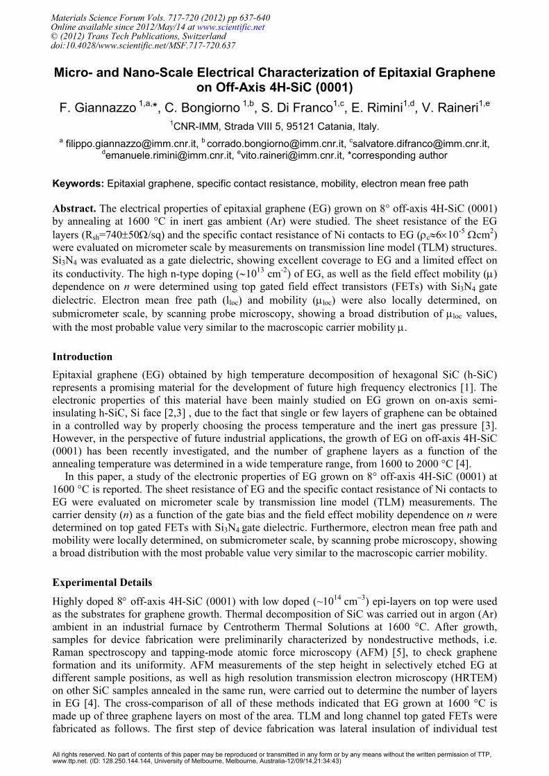
deposited on a laterally insulated rectangular graphene area. Fig.1(a) shows an optical microscopy
image of two TLM structures. In Fig.1(b), the I-V curves measured between pads with different
separations are reported, showing the Ohmic behavior of Ni/EG contacts. Finally, in Fig.1(c) the
resistance RT between two adjacent metal pads is reported as a function of the distance d.
Rsh=740±50Ω/ as well as the contact resistance RC=14±5Ω were determined by fitting of the data
with the linear relation RT=2RC+Rshd/W. The specific contact resistance ρc (independent of pad
geometry) can be obtained as ρc= RCWLT, with LT being the transfer length, i.e. the effective length
of graphene under the pads involved in current transfer from the contact to graphene and from
graphene to the contact. According to the TLM theory, LT2=(ρc/Rsh’), where Rsh’ is the sheet
resistance of graphene under the metal [6]. Due to the charge transfer from metal to the few layers
of graphene [7], Rsh’ can be very different than Rsh in EG between the pads. As discussed in the
following, EG exhibits an overall n-type doping (≈1013
cm-2
) induced by the presence of a buffer
layer at the interface with SiC [5]. This doping is spread between the 3 graphene layers (higher in
the layer closest to the buffer layer, lower in the topmost one). However, in graphene regions coated
by Ni, the work-function difference between the metal and graphene (WNi-WGr≈1eV) causes a
positive charge transfer to EG [8], leading to a counter doping effect, especially in the topmost
graphene layer. This results in an increase of the sheet resistance of EG under the Ni contact.
Taking into account these issues, Rsh’=1160±50Ω/, LT=2.4±0.8µm and ρc=(6.7±4.8)×10-5
Ωcm2
were estimated.
Fig.1 (a) Optical microscopy of two TLM structures. (b) I-V curves measured between pads
with different spacings d. (c) Linear fit of the resistance RT between two adjacent metal pads
as a function of d, yielding the sheet resistance of EG and the contact resistance.
d (µm)
80
100
d (µm)
20
40
60
-30 -15 0 15 30-0.10
-0.05
0.00
0.05
0.10
V(mV)
I(mA)
0 20 40 60 80 1000
100
200
300
400
500R
sh=740±50 Ω/sq
RC=14±5 Ω
RT (
Ω)
d (µm)(b) (c)
200 µm (a)
d (µm)
80
100
d (µm)
20
40
60
-30 -15 0 15 30-0.10
-0.05
0.00
0.05
0.10
V(mV)
I(mA)
0 20 40 60 80 1000
100
200
300
400
500R
sh=740±50 Ω/sq
RC=14±5 Ω
RT (
Ω)
d (µm)(b) (c)
200 µm200 µm200 µm (a)
638 Silicon Carbide and Related Materials 2011
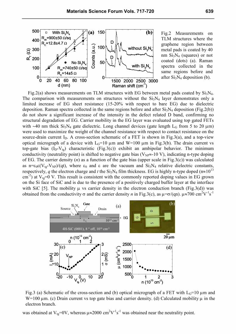
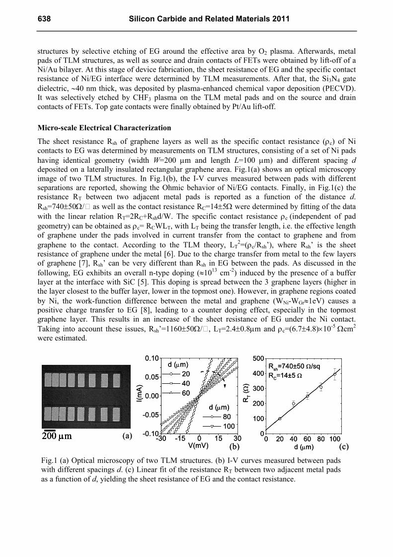
Fig.2(a) shows measurements on TLM structures with EG between metal pads coated by Si3N4.
The comparison with measurements on structures without the Si3N4 layer demonstrates only a
limited increase of EG sheet resistance (15-20% with respect to bare EG) due to dielectric
deposition. Raman spectra collected in the same regions before and after Si3N4 deposition (Fig.2(b))
do not show a significant increase of the intensity in the defect related D band, confirming no
structural degradation of EG. Carrier mobility in the EG layer was evaluated using top gated FETs
with ∼40 nm thick Si3N4 gate dielectric. Long channel devices (gate length LG from 5 to 20 µm)
were used to maximize the weight of the channel resistance with respect to contact resistance on the
source-drain current ID. A cross-section schematic of a FET is shown in Fig.3(a), and a top-view
optical micrograph of a device with LG=10 µm and W=100 µm in Fig.3(b). The drain current vs
top-gate bias (ID-Vtg) characteristic (Fig.3(c)) exhibit an ambipolar behavior. The minimum
conductivity (neutrality point) is shifted to negative gate bias (VNP≈-10 V), indicating n-type doping
of EG. The carrier density (n) as a function of the gate bias (upper scale in Fig.3(c)) was calculated
as n=ε0ε(Vtg-VNP)/(qt), where ε0 and ε are the vacuum and Si3N4 relative dielectric constants,
respectively, q the electron charge and t the Si3N4 film thickness. EG is highly n-type doped (n≈1013
cm-2
) at Vtg=0 V. This result is consistent with the commonly reported doping values in EG grown
on the Si face of SiC and is due to the presence of a positively charged buffer layer at the interface
with SiC [5]. The mobility µ vs carrier density in the electron conduction branch (Fig.3(d)) was
obtained from the conductivity σ and the carrier density n in Fig.3(c), as µ=σ/(qn). µ≈700 cm2V
-1s
-1
was obtained at Vtg=0V, whereas µ≈2000 cm2V
-1s
-1 was obtained near the neutrality point.
Fig.2 Measurements on
TLM structures where the
graphene region between
metal pads is coated by 40
nm Si3N4 (squares) or not
coated (dots) (a). Raman
spectra collected in the
same regions before and
after Si3N4 deposition (b). 1500 2000 2500 3000
0
50
100
150
with Si3N
4
D
D
without Si3N
4
Counts (a.u.)
Raman shift (cm-1)
0 20 40 60 80 1000
100
200
300
400
500 With Si3N
4
Rsh=900±50 Ω/sq
RC=12.8±4.7 Ω
No Si3N
4
Rsh=740±50 Ω/sq
RC=14±5 Ω
RT (
Ω)
d (nm)
(a) (b)
1500 2000 2500 30000
50
100
150
with Si3N
4
D
D
without Si3N
4
Counts (a.u.)
Raman shift (cm-1)
0 20 40 60 80 1000
100
200
300
400
500 With Si3N
4
Rsh=900±50 Ω/sq
RC=12.8±4.7 Ω
No Si3N
4
Rsh=740±50 Ω/sq
RC=14±5 Ω
RT (
Ω)
d (nm)
(a) (b)
Fig.3 (a) Schematic of the cross-section and (b) optical micrograph of a FET with LG=10 µm and
W=100 µm. (c) Drain current vs top gate bias and carrier density. (d) Calculated mobility µ in the
electron branch.
20 µm
(b)
0 1 2 3500
1000
1500
2000
2500
n (1013 cm
-2)
µ (cm
2V
-1s-1) (d)
Gate
DrainSource
EG
Si3N
4
4H-SiC (0001), 8 ° off, 1018 cm-3
1014 cm-3
(a)
-20 -10 0 10 200
10
20
30
Vtg (V)
I d (mA)
0 1 2
0
1
2
3
n (1013 cm
-2)
σ (mS)
(c)
VNP
20 µm 20 µm 20 µm
(b)
0 1 2 3500
1000
1500
2000
2500
n (1013 cm
-2)
µ (cm
2V
-1s-1) (d)
Gate
DrainSource
EG
Si3N
4
4H-SiC (0001), 8 ° off, 1018 cm-3
1014 cm-3
Gate
DrainSource
EG
Si3N
4
4H-SiC (0001), 8 ° off, 1018 cm-3
1014 cm-3
(a)
-20 -10 0 10 200
10
20
30
Vtg (V)
I d (mA)
0 1 2
0
1
2
3
n (1013 cm
-2)
σ (mS)
(c)
VNP
Materials Science Forum Vols. 717-720 639
Nano-scale Electrical Characterization
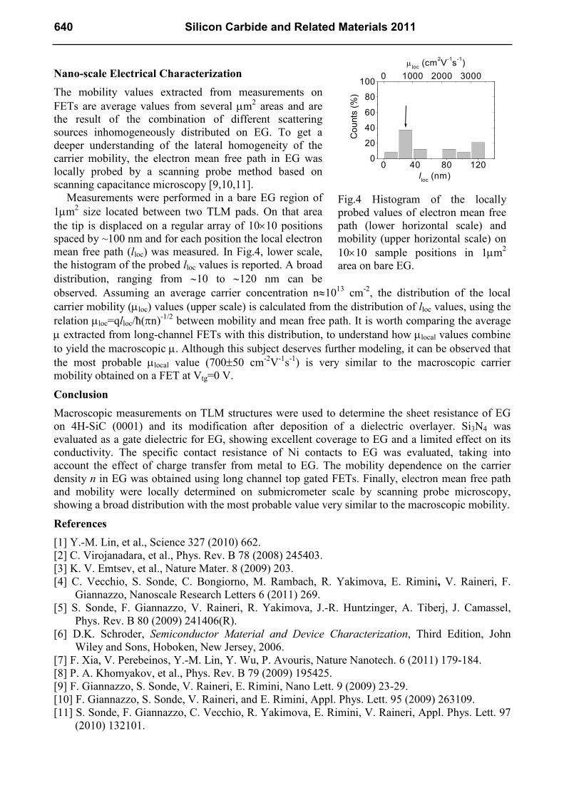
The mobility values extracted from measurements on
FETs are average values from several µm2 areas and are
the result of the combination of different scattering
sources inhomogeneously distributed on EG. To get a
deeper understanding of the lateral homogeneity of the
carrier mobility, the electron mean free path in EG was
locally probed by a scanning probe method based on
scanning capacitance microscopy [9,10,11].
Measurements were performed in a bare EG region of
1µm2 size located between two TLM pads. On that area
the tip is displaced on a regular array of 10×10 positions
spaced by ~100 nm and for each position the local electron
mean free path (lloc) was measured. In Fig.4, lower scale,
the histogram of the probed lloc values is reported. A broad
distribution, ranging from ∼10 to ∼120 nm can be
observed. Assuming an average carrier concentration n≈1013
cm-2
, the distribution of the local
carrier mobility (µloc) values (upper scale) is calculated from the distribution of lloc values, using the
relation µloc=qlloc/ħ(πn)-1/2
between mobility and mean free path. It is worth comparing the average
µ extracted from long-channel FETs with this distribution, to understand how µlocal values combine
to yield the macroscopic µ. Although this subject deserves further modeling, it can be observed that
the most probable µlocal value (700±50 cm-2
V-1
s-1
) is very similar to the macroscopic carrier
mobility obtained on a FET at Vtg=0 V.
Conclusion
Macroscopic measurements on TLM structures were used to determine the sheet resistance of EG
on 4H-SiC (0001) and its modification after deposition of a dielectric overlayer. Si3N4 was
evaluated as a gate dielectric for EG, showing excellent coverage to EG and a limited effect on its
conductivity. The specific contact resistance of Ni contacts to EG was evaluated, taking into
account the effect of charge transfer from metal to EG. The mobility dependence on the carrier
density n in EG was obtained using long channel top gated FETs. Finally, electron mean free path
and mobility were locally determined on submicrometer scale by scanning probe microscopy,
showing a broad distribution with the most probable value very similar to the macroscopic mobility.
References
[1] Y.-M. Lin, et al., Science 327 (2010) 662.
[2] C. Virojanadara, et al., Phys. Rev. B 78 (2008) 245403.
[3] K. V. Emtsev, et al., Nature Mater. 8 (2009) 203.
[4] C. Vecchio, S. Sonde, C. Bongiorno, M. Rambach, R. Yakimova, E. Rimini, V. Raineri, F.
Giannazzo, Nanoscale Research Letters 6 (2011) 269.
[5] S. Sonde, F. Giannazzo, V. Raineri, R. Yakimova, J.-R. Huntzinger, A. Tiberj, J. Camassel,
Phys. Rev. B 80 (2009) 241406(R).
[6] D.K. Schroder, Semiconductor Material and Device Characterization, Third Edition, John
Wiley and Sons, Hoboken, New Jersey, 2006.
[7] F. Xia, V. Perebeinos, Y.-M. Lin, Y. Wu, P. Avouris, Nature Nanotech. 6 (2011) 179-184.
[8] P. A. Khomyakov, et al., Phys. Rev. B 79 (2009) 195425.
[9] F. Giannazzo, S. Sonde, V. Raineri, E. Rimini, Nano Lett. 9 (2009) 23-29.
[10] F. Giannazzo, S. Sonde, V. Raineri, and E. Rimini, Appl. Phys. Lett. 95 (2009) 263109.
[11] S. Sonde, F. Giannazzo, C. Vecchio, R. Yakimova, E. Rimini, V. Raineri, Appl. Phys. Lett. 97
(2010) 132101.
Fig.4 Histogram of the locally
probed values of electron mean free
path (lower horizontal scale) and
mobility (upper horizontal scale) on
10×10 sample positions in 1µm2
area on bare EG.
0
20
40
60
80
1000 1000 2000 3000
Counts (%)
µloc (cm
2V
-1s-1)
0 40 80 120
lloc (nm)
640 Silicon Carbide and Related Materials 2011

Silicon Carbide and Related Materials 2011 10.4028/www.scientific.net/MSF.717-720 Micro- and Nano-Scale Electrical Characterization of Epitaxial Graphene on Off-Axis 4H-SiC (0001) 10.4028/www.scientific.net/MSF.717-720.637
DOI References
[1] Y. -M. Lin, et al., Science 327 (2010) 662.
http://dx.doi.org/10.1126/science.1184289 [2] C. Virojanadara, et al., Phys. Rev. B 78 (2008) 245403.
http://dx.doi.org/10.1103/PhysRevB.78.245403 [3] K. V. Emtsev, et al., Nature Mater. 8 (2009) 203.
http://dx.doi.org/10.1038/nmat2382 [4] C. Vecchio, S. Sonde, C. Bongiorno, M. Rambach, R. Yakimova, E. Rimini, V. Raineri, F. Giannazzo,
Nanoscale Research Letters 6 (2011) 269.
http://dx.doi.org/10.1186/1556-276X-6-269 [5] S. Sonde, F. Giannazzo, V. Raineri, R. Yakimova, J. -R. Huntzinger, A. Tiberj, J. Camassel, Phys. Rev. B
80 (2009) 241406(R).
http://dx.doi.org/10.1103/PhysRevB.80.241406 [7] F. Xia, V. Perebeinos, Y. -M. Lin, Y. Wu, P. Avouris, Nature Nanotech. 6 (2011) 179-184.
http://dx.doi.org/10.1038/nnano.2011.6 [8] P. A. Khomyakov, et al., Phys. Rev. B 79 (2009) 195425.
http://dx.doi.org/10.1103/PhysRevB.79.195425 [9] F. Giannazzo, S. Sonde, V. Raineri, E. Rimini, Nano Lett. 9 (2009) 23-29.
http://dx.doi.org/10.1021/nl801823n [10] F. Giannazzo, S. Sonde, V. Raineri, and E. Rimini, Appl. Phys. Lett. 95 (2009) 263109.
http://dx.doi.org/10.1063/1.3280860