Laboratorio II, modulo 2 2016-2017 - fisgeo.unipg.itduranti/Sito/LaboratorioII-Modulo2... ·...
16
Laboratorio II, modulo 2 2016-2017 Comparatore e FlashADC con l’Op.Amp. “TDC” con l’FPGA LM35 (cfr. http://www.circuitstoday.com/voltage-comparator http://www.seas.upenn.edu/~ese206/labs/adc206/adc206.html https://indico.cern.ch/event/357886/contributions/849365/ attachments/1145718/1648596/FPGA_1.pdf )
-
Upload
truongthuy -
Category
Documents
-
view
219 -
download
2
Transcript of Laboratorio II, modulo 2 2016-2017 - fisgeo.unipg.itduranti/Sito/LaboratorioII-Modulo2... ·...

Laboratorio II, modulo 2 ���2016-2017
Comparatore e FlashADC con l’Op.Amp. “TDC” con l’FPGA
LM35 (cfr. http://www.circuitstoday.com/voltage-comparator
http://www.seas.upenn.edu/~ese206/labs/adc206/adc206.html https://indico.cern.ch/event/357886/contributions/849365/
attachments/1145718/1648596/FPGA_1.pdf)
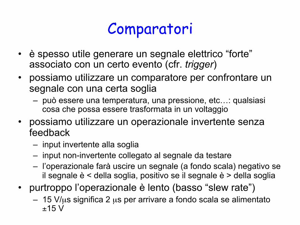
Comparatori • è spesso utile generare un segnale elettrico “forte”
associato con un certo evento (cfr. trigger) • possiamo utilizzare un comparatore per confrontare un
segnale con una certa soglia – può essere una temperatura, una pressione, etc…: qualsiasi
cosa che possa essere trasformata in un voltaggio • possiamo utilizzare un operazionale invertente senza
feedback – input invertente alla soglia – input non-invertente collegato al segnale da testare – l’operazionale farà uscire un segnale (a fondo scala) negativo se
il segnale è < della soglia, positivo se il segnale è > della soglia • purtroppo l’operazionale è lento (basso “slew rate”)
– 15 V/µs significa 2 µs per arrivare a fondo scala se alimentato ±15 V

Esempio (reale) di comparatore
• quando Vin < Vref, Vout è “pulled-up” (attraverso il resistore di “pull-up”, usualmente 1 kΩ o più) – questa configurazione è chiamata a “collettore aperto”: l’uscita è il
collettore di un transistor npn. In saturazione è tirata verso l’emettitore (ground), ma se non c’è corrente di base il collettore è tirato al voltaggio di pull-up
• l’uscita è una versione “digitale” del segnale – i valori “alto” e “basso” sono configurabili (ground e 5V, nell’esempio)
• possono essere utili anche per convertire un segnale “lento” in uno “veloce” – se è necessatia una maggiore precisione di “timing”
+
- Vref
Vin Vout
+5 V
R 5 V
Vref
Vout
Vin
tempo
V

Comparatore con l’operazionale
• Vref realizzato con un partitore resistivo fra V+ (che è anche l’alimentazione positiva dell’operazionale) e terra
• in regime di open-loop, Vout passerà da V+ (per Vin>Vref) a V- (per Vin<Vref) • montaggio di Fig.1 è non invertente e ha Vin nell’input con impedenza più
alta • montaggio di Fig.2 è invertente e ha Vin nell’input con impedenza più bassa
Vref Vref
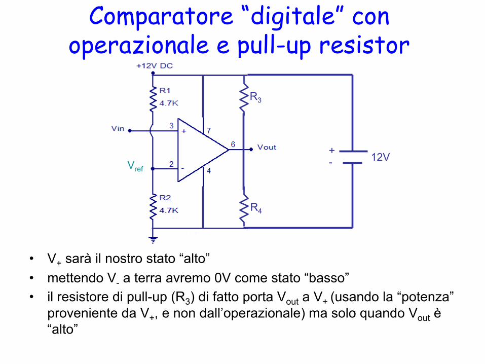
Comparatore “digitale” con operazionale e pull-up resistor
• V+ sarà il nostro stato “alto” • mettendo V- a terra avremo 0V come stato “basso” • il resistore di pull-up (R3) di fatto porta Vout a V+ (usando la “potenza”
proveniente da V+, e non dall’operazionale) ma solo quando Vout è “alto”
Vref
R3
R4
+ - 12V

Comparatore “digitale” con operazionale e pull-up resistor + LED
• possiamo aggiungere un LED per “indicare” quando la soglia, Vref, è passata
Vref
R3
R4
+ - 12V

Comparatore “digitale” con operazionale 741 e pull-up resistor + LED
• in realtà l’op.amp. 741 NON può essere utilizzato in modalità unipolare (alimentandolo solo da un lato) e quindi se si mette V- a terra in realtà l’op.amp. non funziona correttamente. à è sufficiente dare un piccolo voltaggio negativo (~ -1V) per vincere il potenziale di contatto delle giunzioni
Vref
R3
R4
~1V - +
+ - 12V
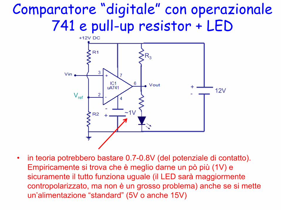
Comparatore “digitale” con operazionale 741 e pull-up resistor + LED
• in teoria potrebbero bastare 0.7-0.8V (del potenziale di contatto). Empiricamente si trova che è meglio darne un pò più (1V) e sicuramente il tutto funziona uguale (il LED sarà maggiormente contropolarizzato, ma non è un grosso problema) anche se si mette un’alimentazione “standard” (5V o anche 15V)
Vref
R3
R4
~1V - +
+ - 12V
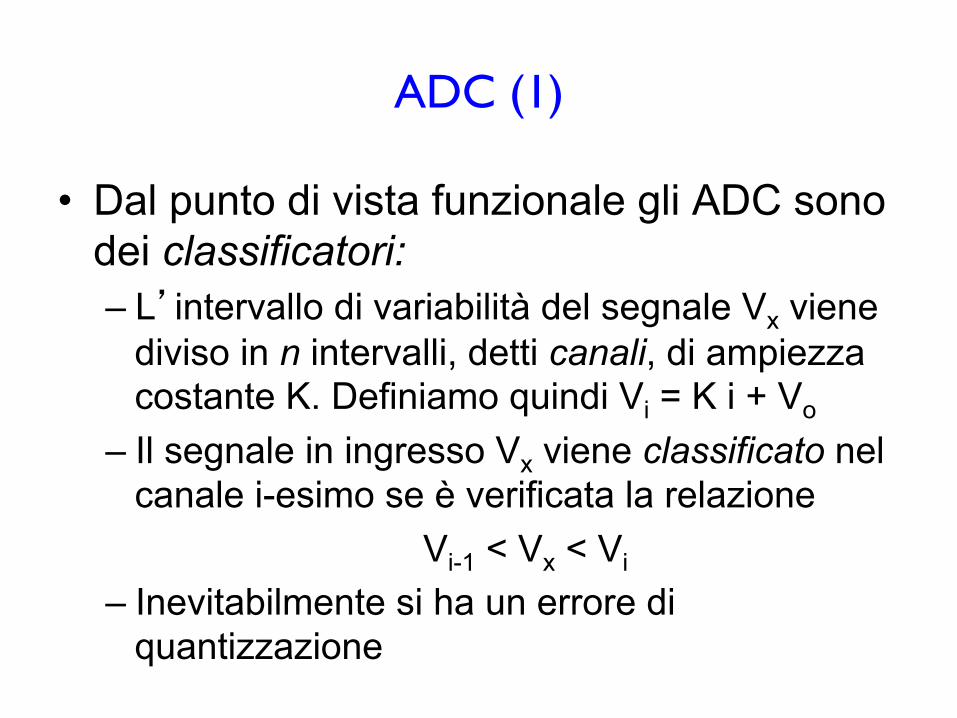
ADC (1)
• Dal punto di vista funzionale gli ADC sono dei classificatori: – L’intervallo di variabilità del segnale Vx viene
diviso in n intervalli, detti canali, di ampiezza costante K. Definiamo quindi Vi = K i + Vo
– Il segnale in ingresso Vx viene classificato nel canale i-esimo se è verificata la relazione
Vi-1 < Vx < Vi – Inevitabilmente si ha un errore di
quantizzazione
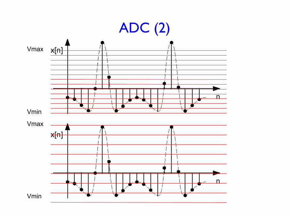
ADC (2)
Vmin
Vmax
Vmin
Vmax
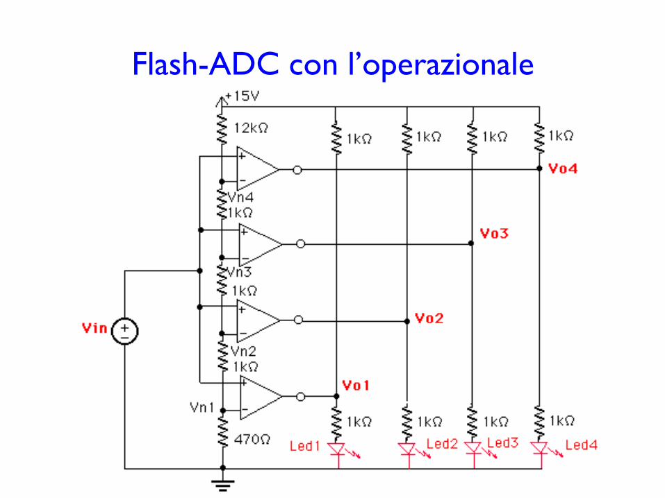
Flash-ADC con l’operazionale

LM35
+VS VOUT GND
+VSVOUT
GND
N.C.N.C.
N.C.N.C.N.C.
1234
8765
+VS VOUTGND
LM35DT
+VS VOUT
GND t
3
LM35www.ti.com SNIS159G –AUGUST 1999–REVISED AUGUST 2016
Product Folder Links: LM35
Submit Documentation FeedbackCopyright © 1999–2016, Texas Instruments Incorporated
5 Pin Configuration and Functions
NDV Package3-Pin TO-CAN(Bottom View)
Case is connected to negative pin (GND)
D Package8-PIN SOIC(Top View)
N.C. = No connection
LP Package3-Pin TO-92(Bottom View)
NEB Package3-Pin TO-220(Top View)
Tab is connected to the negative pin(GND).NOTE: The LM35DT pinout is different thanthe discontinued LM35DP
Pin FunctionsPIN
TYPE DESCRIPTIONNAME TO46 TO92 TO220 SO8VOUT — — — 1 O Temperature Sensor Analog Output
N.C.— — — 2
— No Connection— — — 3
GND — — — 4 GROUND Device ground pin, connect to power supply negativeterminal
N.C.— — — 5
— No Connection— — — 6— — — 7
+VS — — — 8 POWER Positive power supply pin
LM35
+VS
R1
VOUT
tVS
LM35
+VS
(4 V to 20 V)
OUTPUT0 mV + 10.0 mV/4C
Product
Folder
Sample &Buy
Technical
Documents
Tools &
Software
Support &Community
An IMPORTANT NOTICE at the end of this data sheet addresses availability, warranty, changes, use in safety-critical applications,intellectual property matters and other important disclaimers. PRODUCTION DATA.
LM35SNIS159G –AUGUST 1999–REVISED AUGUST 2016
LM35 Precision Centigrade Temperature Sensors
1
1 Features1• Calibrated Directly in Celsius (Centigrade)• Linear + 10-mV/°C Scale Factor• 0.5°C Ensured Accuracy (at 25°C)• Rated for Full −55°C to 150°C Range• Suitable for Remote Applications• Low-Cost Due to Wafer-Level Trimming• Operates from 4 V to 30 V• Less than 60-μA Current Drain• Low Self-Heating, 0.08°C in Still Air• Non-Linearity Only ±¼°C Typical• Low-Impedance Output, 0.1 Ω for 1-mA Load
2 Applications• Power Supplies• Battery Management• HVAC• Appliances
3 DescriptionThe LM35 series are precision integrated-circuittemperature devices with an output voltage linearly-proportional to the Centigrade temperature. TheLM35 device has an advantage over lineartemperature sensors calibrated in Kelvin, as the useris not required to subtract a large constant voltagefrom the output to obtain convenient Centigradescaling. The LM35 device does not require anyexternal calibration or trimming to provide typicalaccuracies of ±¼°C at room temperature and ±¾°Cover a full −55°C to 150°C temperature range. Lowercost is assured by trimming and calibration at thewafer level. The low-output impedance, linear output,and precise inherent calibration of the LM35 devicemakes interfacing to readout or control circuitryespecially easy. The device is used with single powersupplies, or with plus and minus supplies. As theLM35 device draws only 60 μA from the supply, it hasvery low self-heating of less than 0.1°C in still air. TheLM35 device is rated to operate over a −55°C to150°C temperature range, while the LM35C device israted for a −40°C to 110°C range (−10° withimproved accuracy). The LM35-series devices areavailable packaged in hermetic TO transistorpackages, while the LM35C, LM35CA, and LM35Ddevices are available in the plastic TO-92 transistorpackage. The LM35D device is available in an 8-leadsurface-mount small-outline package and a plasticTO-220 package.
Device Information(1)
PART NUMBER PACKAGE BODY SIZE (NOM)
LM35
TO-CAN (3) 4.699 mm × 4.699 mmTO-92 (3) 4.30 mm × 4.30 mmSOIC (8) 4.90 mm × 3.91 mmTO-220 (3) 14.986 mm × 10.16 mm
(1) For all available packages, see the orderable addendum atthe end of the datasheet.
Basic Centigrade Temperature Sensor(2°C to 150°C) Full-Range Centigrade Temperature Sensor
Choose R1 = –VS / 50 µAVOUT = 1500 mV at 150°CVOUT = 250 mV at 25°CVOUT = –550 mV at –55°C
LM35
+VS
R1
VOUT
tVS
LM35
+VS
(4 V to 20 V)
OUTPUT0 mV + 10.0 mV/4C
Product
Folder
Sample &Buy
Technical
Documents
Tools &
Software
Support &Community
An IMPORTANT NOTICE at the end of this data sheet addresses availability, warranty, changes, use in safety-critical applications,intellectual property matters and other important disclaimers. PRODUCTION DATA.
LM35SNIS159G –AUGUST 1999–REVISED AUGUST 2016
LM35 Precision Centigrade Temperature Sensors
1
1 Features1• Calibrated Directly in Celsius (Centigrade)• Linear + 10-mV/°C Scale Factor• 0.5°C Ensured Accuracy (at 25°C)• Rated for Full −55°C to 150°C Range• Suitable for Remote Applications• Low-Cost Due to Wafer-Level Trimming• Operates from 4 V to 30 V• Less than 60-μA Current Drain• Low Self-Heating, 0.08°C in Still Air• Non-Linearity Only ±¼°C Typical• Low-Impedance Output, 0.1 Ω for 1-mA Load
2 Applications• Power Supplies• Battery Management• HVAC• Appliances
3 DescriptionThe LM35 series are precision integrated-circuittemperature devices with an output voltage linearly-proportional to the Centigrade temperature. TheLM35 device has an advantage over lineartemperature sensors calibrated in Kelvin, as the useris not required to subtract a large constant voltagefrom the output to obtain convenient Centigradescaling. The LM35 device does not require anyexternal calibration or trimming to provide typicalaccuracies of ±¼°C at room temperature and ±¾°Cover a full −55°C to 150°C temperature range. Lowercost is assured by trimming and calibration at thewafer level. The low-output impedance, linear output,and precise inherent calibration of the LM35 devicemakes interfacing to readout or control circuitryespecially easy. The device is used with single powersupplies, or with plus and minus supplies. As theLM35 device draws only 60 μA from the supply, it hasvery low self-heating of less than 0.1°C in still air. TheLM35 device is rated to operate over a −55°C to150°C temperature range, while the LM35C device israted for a −40°C to 110°C range (−10° withimproved accuracy). The LM35-series devices areavailable packaged in hermetic TO transistorpackages, while the LM35C, LM35CA, and LM35Ddevices are available in the plastic TO-92 transistorpackage. The LM35D device is available in an 8-leadsurface-mount small-outline package and a plasticTO-220 package.
Device Information(1)
PART NUMBER PACKAGE BODY SIZE (NOM)
LM35
TO-CAN (3) 4.699 mm × 4.699 mmTO-92 (3) 4.30 mm × 4.30 mmSOIC (8) 4.90 mm × 3.91 mmTO-220 (3) 14.986 mm × 10.16 mm
(1) For all available packages, see the orderable addendum atthe end of the datasheet.
Basic Centigrade Temperature Sensor(2°C to 150°C) Full-Range Centigrade Temperature Sensor
Choose R1 = –VS / 50 µAVOUT = 1500 mV at 150°CVOUT = 250 mV at 25°CVOUT = –550 mV at –55°C
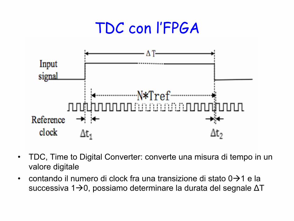
TDC con l’FPGA
• TDC, Time to Digital Converter: converte una misura di tempo in un valore digitale
• contando il numero di clock fra una transizione di stato 0à1 e la successiva 1à0, possiamo determinare la durata del segnale ΔT
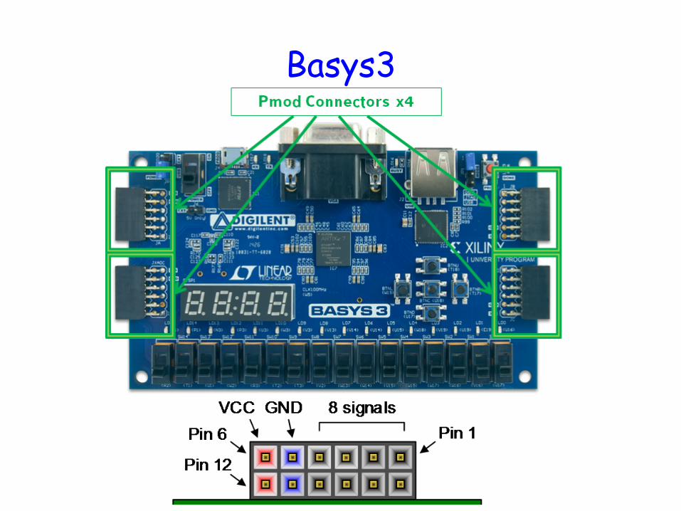
Basys3

Basys3

• TTL: Transistor-Transistor Logic, basato sul BJT – output: ‘1’ logico: VOH > 3.3 V; ‘0’ logico: VOL < 0.35 V – input: ‘1’ logico: VIH > 2.0 V; ‘0’ logico: VIL < 0.8 V – zona “morta” fra 0.8V e 2.0 V
TTL