
SINGLE EVENT EFFECTS ON FPGAs -...
117
UNIVERSITÀ DI PADOVA FACOLTÀ DI INGEGNERIA Dipartimento di Ingegneria dell’Informazione Scuola di Dottorato di Ricerca in Ingegneria dell’Informazione Indirizzo: Scienza e Tecnologia dell’Informazione CICLO XXII SINGLE EVENT EFFECTS ON FPGAs Direttore della Scuola: Ch.mo Prof. Matteo Bertocco Supervisore: Ch.mo Prof. Alessandro Paccagnella Dottorando: Andrea Manuzzato
-
Upload
duongxuyen -
Category
Documents
-
view
216 -
download
0
Transcript of SINGLE EVENT EFFECTS ON FPGAs -...

UNIVERSITÀ DI PADOVA
FACOLTÀ DI INGEGNERIA
Dipartimento di Ingegneria dell’Informazione
Scuola di Dottorato di Ricerca in Ingegneria dell’Informazione
Indirizzo: Scienza e Tecnologia dell’Informazione
CICLO XXII
SINGLE EVENT EFFECTS
ON
FPGAs
Direttore della Scuola: Ch.mo Prof. Matteo Bertocco
Supervisore: Ch.mo Prof. Alessandro Paccagnella
Dottorando: Andrea Manuzzato

Sommario
Le Field Programmable Gate Array (FPGA) sin dalla loro introduzione nel
mercato presentarono un modo davvero innovativo nell’implementazione di circuiti
hardware. La proprietà fondamentale di questi circuiti integrati è la possibilità di
personalizzazione delle funzionalità dopo il processo produttivo da parte
dell’utente finale. L’architettura generale di una FPGA è composta di elementi
configurabili che possono essere programmati per implementare funzionalità base
di logica combinatoria e/o sequenziale. Una struttura configurabile
d’interconnessioni permette di connettere questi elementi per l’implementazione di
circuiti complessi. Inoltre, blocchi di input/output gestiscono l’interfacciamento
con il mondo esterno, permettendo la possibilità di configurare vari livelli di
tensione e standard di comunicazione. Questa tipologia di dispositivi offre una
flessibilità estrema e possono essere riprogrammati anche nel sistema finale, quindi
permettendo di rendere un design esistente conforme a nuovi requisiti, migliorarlo
o addirittura correggere errori progettuali. I circuiti possono essere descritti
utilizzando linguaggi ad alto livello e la loro implementazione, non richiede il
lungo e costoso processo di design come per la tecnologia ASIC. Gli sviluppatori
possono usare il medesimo ambiente di sviluppo e linguaggio di descrizione per
diversi progetti e differenti dispositivi (dello stesso produttore) fornendo rapidi
tempi d’ingegnerizzazione per collocare il prodotto sul mercato. La flessibilità è
ottenuta memorizzando le informazioni della configurazione del dispositivo per
implementare il circuito desiderato in una memoria dedicata, detta di
configurazione. In base alla tecnologia utilizzata per la memoria, si possono
distinguere FPGA basate su memoria RAM statica e quelle basate su memoria
flash non volatile.
Tutte queste proprietà hanno diffuso l’utilizzo delle FPGA in vari settori
anche per applicazioni operanti in ambienti soggetti a livelli di radiazione e per
applicazioni safety-critical. A esempio, in ambito spaziale, l’utilizzo delle FPGA è
in costante incremento in quanto questi dispositivi possono adempiere la costante
crescita di richiesta di calcolo computazionale (come nelle applicazioni di
elaborazione digitale delle immagini e di telecomunicazione) e le proprietà di ri-
configurabilità possono estendere la vita di un’applicazione.
Sfortunatamente, un grosso svantaggio di questi dispositivi è la loro
sensibilità agli effetti della radiazione. Inoltre, l’evoluzione della tecnologia e allo

stesso tempo l’introduzione di nuovi materiali e nuove strutture stanno esacerbando
problemi di affidabilità riguardanti la radiazione. Una citazione di Rober Baumann,
fellow IEEE, chiaramente esprime i problemi di affidabilità riguardanti la
radiazione:
“Gli errori indotti dalla radiazione inducono un tasso di errore più alto di
tutti gli altri meccanismi relativi affidabilità messi assieme”
Gli effetti indotti dalla radiazione in questi dispositivi dipendono da vari
fattori: in particolare dalla tecnologia usata per la memoria di configurazione e il
nodo tecnologico utilizzato per la produzione. In questo scenario è davvero
importante capire le modalità di fallimento delle FPGA, in modo tale da fornire la
più appropriata tecnica di irrobustimento ai fini di preservare la corretta
funzionalità del circuito implementato.
Scopo di questa tesi è lo studio degli effetti indotti dalla radiazione su
FPGA. Testare la sensibilità della radiazione per questi dispositivi è un processo
complesso. Prima di tutto, specifiche piattaforme devono essere sviluppate per
monitorare i funzionamenti del dispositivo e del circuito implementato sotto
irraggiamento. Inoltre, l’analisi dei dati non è immediata a causa di mancanza di
dettagliate informazioni sul layout fisico da parte dei produttori. In questo lavoro
sono presentate delle complete metodologie per lo studio degli effetti di radiazione,
analizzando gli errori indotti e codificando le risorse interne affette.
Dettagliate analisi delle modalità di guasto sono state svolte: in particolare
questo lavoro focalizza su due differenti tecnologie di FPGA:
FPGA basate su RAM statica come i dispositivi Spartan-3 prodotti da
Xilinx;
FPGA basate su memoria Flash come i dispositivi ProAsic3 prodotti da
Actel.
Questi dispositivi utilizzano differenti tipologie di memoria per mantenere
la configurazione interna e quindi, differenti fenomeni affliggono le due famiglie di
FPGA.
In seguito allo studio degli eventi indotti dalla radiazione, sono presentate
analisi di alcune tecniche di mitigazione a livello di design. In particolare, ci siamo
focalizzati nella ridondanza tripla modulare (TMR) e sistemi numerici ridondanti
basati sui residui (RRNS) implementati in FPGA basate su RAM statica. L’intento
di entrambe le tecniche è incrementare l’affidabilità dell’applicazione utilizzando
informazioni addizionali per rivelare e mascherare i guasti al mondo esterno.
I lavori presentati sono stati resi possibili grazie alla collaborazione con il
Politecnico di Torino e l’università di Roma Tor Vergata.
La tesi è organizzata come segue:
Il Capitolo 1 presenta una breve panoramica della radiazione e i suoi effetti
nell’elettronica;
Il Capitolo 2 presenta gli effetti della radiazione su FPGA basate su
memoria RAM statica. In particolare sono presentati esperimenti per capire
e analizzare le modalità di guasto indotte dalla radiazione. I test eseguiti
hanno utilizzato dispositivi Xilinx Spartan-3 che sono stati irraggiati con
neutroni, ioni pesanti e particelle alfa;
Nel Capitolo 3 sono presentati studi riguardanti tecniche di irrobustimento
a livello di design per circuiti implementati in FPGA basate su RAM
statica. L’impatto dell’accumulo di errori nella memoria di configurazione
è stato analizzato in funzione a differenti schemi d’implementazione della
ridondanza tripla modulare. Inoltre, una tecnica di irrobustimento basata
sull’aritmetica modulare (RRNS) è presentata per implementare un filtro
totalmente tollerante ai guasti. Il capitolo conclude proponendo una
metodologia per lo studio dell’impatto di eventi multipli in circuiti TMR;
Il Capitolo 4 verte sullo studio degli effetti da evento singolo per FPGA
basate su memoria di tipo flash. Il particolare evento studiato su questi
dispositivi è il fenomeno dei transienti. Sono presentati test
d’irraggiamento per la misura della durata dei transienti indotti dalla
radiazione. Nell’ultima parte del capitolo sono riportati ulteriori
esperimenti per stimare l’impatto dei transienti indotti su circuiti simili a
quelli realmente utilizzati (ossia, diversi da specifiche strutture di test).
Il Capito 5 conclude la tesi discutendo in modo generale i risultati raccolti
in questo lavoro.


Table of Contents
Summary .............................................................................................................. i
Chapter 1 Radiation - Overview ....................................................................... 1 1.1 Types of radiations .......................................................................................... 1 1.2 Radiation environments .................................................................................. 2
1.2.1 Space Radiation Environment ........................................................................ 2 1.2.2 Terrestrial Radiation Environment ................................................................. 5
1.3 Radiation – Interaction with Electronics ...................................................... 8 1.3.1 Single Event Effects ....................................................................................... 8 1.3.2 Classification .................................................................................................. 9 1.3.3 Total Ionizing Dose ...................................................................................... 10
1.4 Indexes of radiation sensitivity ..................................................................... 11
Chapter 2 Radiation Effects on SRAM-based FPGAs .................................. 13 2.1 FPGA Architecture ............................................................................................ 13 2.2 FPGA Configuration ......................................................................................... 17 2.3 SEE in SRAM-based FPGA .............................................................................. 18 2.4 Radiation sensitivity: test methodologies ......................................................... 20 2.5 Radiation Tests ................................................................................................... 21
2.5.1 Neutron Experiment ..................................................................................... 21 2.5.1 Heavy-ion irradiation .................................................................................... 30 2.5.2 Total Dose and Soft Error Rate .................................................................... 35
Chapter 3 Hardening-by-design techniques for SRAM-based FPGAs ....... 37 3.1 Hardening Techniques ...................................................................................... 38 3.2 Triple Modular Redundancy ............................................................................ 39
3.2.1 X-TMR ......................................................................................................... 39 3.2.2 Partial TMR .................................................................................................. 41 3.2.3 Problems for TMR implementation .............................................................. 42
3.3 Experimental study of TMR in presence of error accumulation ................... 44 3.3.1 Experimental Setup and Devices .................................................................. 44 3.3.2 Tested Configurations and Circuits .............................................................. 45 3.3.3 Experimental Results .................................................................................... 46 3.3.4 Analytical Model .......................................................................................... 48
3.4 Redundant Residue Number System ............................................................... 53 3.4.1 Residue Number System Background .......................................................... 53 3.4.2 Totally fault tolerant RNS FIR filter ............................................................ 56 3.4.3 Experimental validation of a totally fault tolerant filter implementation ..... 58
3.5 Multiple Bit Upsets in TMR circuits ................................................................ 61

3.5.1 Analysis Methodology .................................................................................. 62 3.5.2 Device characterization using laser testing .................................................. 62 3.5.3 Layout-aware Static Analyzer for MBUs ..................................................... 64 3.5.4 Analysis of Errors Produced by MBUs ........................................................ 66 3.5.5 Experimental Results .................................................................................... 69
Chapter 4 Radiation effects on Flash-based FPGAs ..................................... 73 4.1 Flash-based FPGAs architecture ...................................................................... 73 4.2 SET pulse width ................................................................................................. 75
4.2.1 Experimental setup for SET pulse width measurement ................................ 77 4.2.2 Transient pulse width - irradiation data ........................................................ 81
4.3 SETs in a real-life circuit ................................................................................... 85 4.3.1 Testing environment ..................................................................................... 86 4.3.2 Routing Modification/Analysis Tools, RMAT ............................................. 88 4.3.3 Experimental Setup ...................................................................................... 90 4.3.4 Experimental Results and Analysis .............................................................. 92
Chapter 5 Conclusion Remark ........................................................................ 95
Bibliography ...................................................................................................... 99

i
Summary
Field Programmable Gate Arrays, FPGAs, since their introduction on the
market presented a very innovative way of implementing hardware designs. The
fundamental property of these integrated circuits is the capability of a user’s
customization after manufacturing. An FPGA’s general architecture is composed of
configurable elements that can be programmed to implement basic combinatorial
and/or sequential logic. Configurable connection architecture can wire the
configurable elements to implement complex circuits. Furthermore, input/output
blocks manage interfacing with the external world, giving an option to configure
various voltage and communication standards. These devices offer an extreme
flexibility because they can be re-programmed in the field, hence they allow to
comply with new needs or to improve an existing design (or even to post-correct
design errors). Circuits can be described using high-level languages without a need
for a long and expensive design process to be implemented as required for ASICs.
Designers can use the same development environments and description languages
through different devices (of the same vendor) and for different projects, providing
very short time to market. Flexibility is obtained storing the device configuration to
implement a desired circuit in a configuration memory, and based on used memory
technology we can identify SRAM-based FPGAs and Flash-based FPGAs.
All these facts have spread FPGA use into various sectors, including harsh
radiation environments and safety-critical applications. For example, in space
application, their use is constantly increasing, because FPGAs can comply with
increasing computational needs – image processing, telecommunication – and their
re-configurability can extend an application’s lifespan.
Unfortunately, a great disadvantage of these devices is their sensitivity to
radiation effects. As well, technology scaling along with the introduction of new
material and new embedded structures is exacerbating radiation reliability issues. A
citation of Robert Baumann, fellow IEEE, clearly expresses the reliability problem
related to radiation:
“Soft errors induce the highest failure rate of all other reliability
mechanisms combined.”
Any radiation-induced effects these devices suffer depend on various
factors. In particular, configuration memory technology and the technological
process node. In this scenario, it is very important to understand failure modes of
ii
FPGAs to provide a more suitable mitigation technique to preserve their correct
circuit functionalities.
This Thesis is a studying of radiation-induced effects on FPGAs. Testing
radiation sensitivity of such devices is a complex process. First, specific platforms
have to be developed to monitor a device’s behavior and its implemented circuit
under a radiation source. Further, data analysis is complicated by a lack of detailed
physical information from manufacturers. In this work, we present complete
experimental methodologies to study radiation effects on FPGAs, analyzing any
induced errors and decoding affected resources.
Detailed analysis of these failure modes has been carried out; in particular,
this work has targeted two different FPGA technologies:
SRAM-based FPGAs, such as Xilinx Spartan-3 devices; and
Flash-based FPGAs, such as Actel ProASIC3 devices.
As their names suggest, these devices use different kinds of memory to
store device configuration, and hence, different phenomena affect these two FPGA
families.
After a review of radiation-induced events, we present an analysis of
mitigation techniques at design level. In particular, we focused on Triple Modular
Redundancy, TMR, and Redundant Residue Number System, RRNS,
implementations in SRAM-based FPGAs. Both techniques intend to increment a
design’s reliability using additional information to detect and mask faults to the
external world.
This presented work has been made possible thanks to collaboration with
Politecnico di Torino and Università Tor Vergata, Rome.
The Thesis is organized as follows:
Chapter 1 is a brief overview of radiation and its effects on
electronics;
Chapter 2 describes radiation-induced effects on SRAM-based
FPGAs. In particular, irradiation experiments to understand and
analyze the induced failure modes are presented. These tests
have focused on Xilinx Spartan-3 devices; we have irradiated
this FPGA with neutrons, heavy ions and alpha particles;
Chapter 3 presents studies on hardening-by-design techniques
implemented in SRAM-based FPGAs. The impact of error
accumulation in their configuration memory is analyzed on
different implementations of the TMR scheme. Furthermore, a
hardening technique based on modular arithmetic, RRNS, to
implement a totally fault-tolerant FIR filter is presented, proving
its effectiveness. Finally, a methodology to study the impact of
multiple bit upsets on TMR circuits is proposed;
Chapter 4 focuses on Single Event Effects on Flash-based
FPGAs. The studied event in this kind of FPGA is the Single

iii
Event Transient phenomenon. Irradiation tests to measure
induced transient pulse width are presented. Further experiments
to assess SET impact in real-like circuits are reported; and
Chapter 5 discusses the results gathered in this work.

iv
Chapter 1 – Radiation overview
1
Chapter 1
Radiation - Overview
In physics, radiation is any process of energy transmission through space
or a medium. In nature, unstable atoms, in the process of reaching a stable
configuration, emit energy in different ways. Radiation can be defined as ionizing
or non-ionizing. An ionizing radiation has enough energy to ionize particles,
generally, stripping electrons from the struck outer shell atoms.
1.1 Types of radiations
Alpha particles are helium nuclei, consisting of two protons and two neutrons.
These particles have high ionizing power, but due to their large mass, they
have low energy and low range ;
Protons carry a unitary charge and have the mass of a hydrogen nucleus. For
their masses, protons are difficult to deflect;
Beta particles, where electrons are lightly ionizing particles. They can
penetrate matter more easily than alpha particles, but can be deflected quite
easily. Their particle mass is the same, but a beta particle has a positive charge;
Gamma Rays/X-Rays are photons or electromagnetic radiation with short-
wavelength. Gamma rays are originated in nuclear interactions, while X-rays
originate from particle collisions. Their interaction with matter for two
radiations is the same — they are highly penetrating and lightly ionizing; and
Neutrons have no charge and hence are very difficult to stop. A neutron mass is
about equal to a proton mass. Neutrons are classified by their energy: fast
neutrons, >100keV, and thermal neutrons, <1eV.

Chapter 1 – Radiation overview
2
1.2 Radiation environments
1.2.1 Space Radiation Environment In outer space radiation environments there are two fundamental radiation
sources – solar and galactic cosmic rays, GCRs. Our sun presents an activity based
on an 11 year cycle with seven years of solar maximum and four years of solar
minimum (Lum, 2004) and at the end of a cycle, the sun inverts the polarity of its
magnetic field. Two kinds of events occur during high solar activity – Coronal
Mass Ejections, CMEs, and solar flares1.
Solar flares are the most explosive events in our solar system. These events
involve regions in the photosphere near sunspots and any emitted particle
composition is rich in heavy ions. CME events take place in the sun chromospheres
and appear as a bubble of gas and magnetic field. About 107
grams of matter is
released into our solar system, and they are proton rich particle events. Events are
classified as gradual or impulsive. The gradual events produce a raised particle flux
that decays slowly over several hours or even days. These events are proton-rich
and can produce high-energy – greater than 30 MeV – proton fluences higher than
109 protons/cm
2 accumulated over a few days. Gradual events are responsible for
the majority of large proton fluence events, and occur at a frequency of about 10
per year during solar maximum conditions. Impulsive events are by definition of
much shorter duration (hours at most), and are marked by increased fluences of
heavy ions and low energy electrons. Impulsive events produce heavy ion fluences
that can be orders of magnitude above the galactic cosmic ray background. These
heavy ions have energies ranging from tens of MeV/nucleon to hundreds of
GeV/nucleon, but at the upper end of this range, the flux falls below the galactic
cosmic ray background.
Galactic Cosmic Rays, GCRs, are particles coming from outer space
(Barth, 1997), (Xapsos, 2006). They present a diffuse background radiation
isotropic in free space regions. Their composition is 83 percent protons, 13 percent
alpha particles, 3 percent electrons and 1 percent heavy ions. Most of these
particles have energy up to 10 GeV/amu, but we can have high-energy particles of
up to 1011
GeV. The flux of GCR reaching Earth is modulated by its solar activity;
in particular, the flux is anti-correlated with solar activity — solar flux scatters
incoming charged particles. At present, there is no clear explanation for this
phenomenon’s origin and its associated energies. A heavy ion component is most
problematic for electronics — they have high energy, hence they are not trapped by
radiation belts and they have high penetration rates. Interacting with Earth’s
1 These events can happen also in solar minimum, but the intensity and the
frequencies are lower.
Chapter 1 – Radiation overview
3
atmosphere, they create a shower of byproducts as presented in the section on the
terrestrial radiation environment.
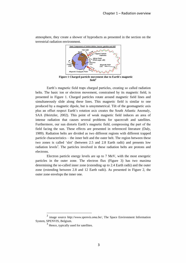
Figure 1 Charged particle movement due to Earth's magnetic
field2
Earth’s magnetic field traps charged particles, creating so called radiation
belts. The basic ion or electron movement, constrained by its magnetic field, is
presented in Figure 1. Charged particles rotate around magnetic field lines and
simultaneously slide along these lines. This magnetic field is similar to one
produced by a magnetic dipole, but is unsymmetrical. Tilt of the geomagnetic axis
plus an offset respect Earth’s rotation axis creates the South Atlantic Anomaly,
SAA (Heirtzler, 2002). This point of weak magnetic field induces an area of
intense radiation that causes several problems for spacecraft and satellites.
Furthermore, our sun distorts Earth’s magnetic field, compressing the part of the
field facing the sun. These effects are presented in referenced literature (Daly,
1989). Radiation belts are divided as two different regions with different trapped
particle characteristics – the inner belt and the outer belt. The region between these
two zones is called ‘slot’ (between 2.5 and 2.8 Earth radii) and presents low
radiation levels3. The particles involved in these radiation belts are protons and
electrons.
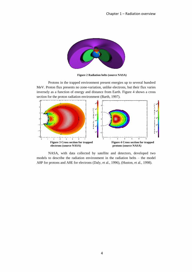
Electron particle energy levels are up to 7 MeV, with the most energetic
particles in the outer zone. The electron flux (Figure 3) has two maxima
determining the so-called inner zone (extending up to 2.4 Earth radii) and the outer
zone (extending between 2.8 and 12 Earth radii). As presented in Figure 2, the
outer zone envelops the inner one.
2 image source http://www.spenvis.oma.be/, The Space Environment Information
System, SPENVIS, Belgium. 3 Hence, typically used for satellites.
Chapter 1 – Radiation overview
4
Figure 2 Radiation belts (source NASA)
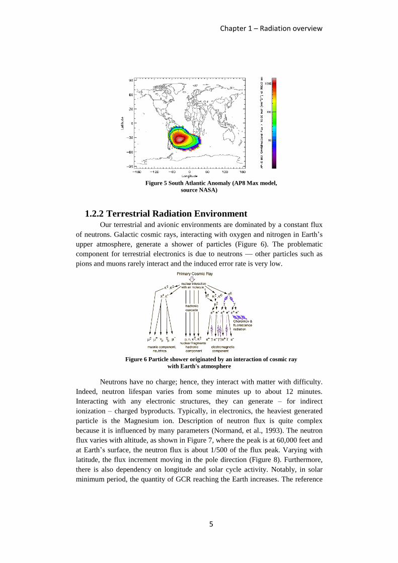
Protons in the trapped environment present energies up to several hundred
MeV. Proton flux presents no zone-variation, unlike electrons, but their flux varies
inversely as a function of energy and distance from Earth. Figure 4 shows a cross
section for the proton radiation environment (Barth, 1997).
Figure 3 Cross section for trapped
electrons (source NASA)
Figure 4 Cross section for trapped
protons (source NASA)
NASA, with data collected by satellite and detectors, developed two
models to describe the radiation environment in the radiation belts – the model
A8P for protons and A8E for electrons (Daly, et al., 1996), (Huston, et al., 1998).
Chapter 1 – Radiation overview
5
Figure 5 South Atlantic Anomaly (AP8 Max model,
source NASA)
1.2.2 Terrestrial Radiation Environment Our terrestrial and avionic environments are dominated by a constant flux
of neutrons. Galactic cosmic rays, interacting with oxygen and nitrogen in Earth’s
upper atmosphere, generate a shower of particles (Figure 6). The problematic
component for terrestrial electronics is due to neutrons — other particles such as
pions and muons rarely interact and the induced error rate is very low.
Figure 6 Particle shower originated by an interaction of cosmic ray
with Earth's atmosphere
Neutrons have no charge; hence, they interact with matter with difficulty.
Indeed, neutron lifespan varies from some minutes up to about 12 minutes.
Interacting with any electronic structures, they can generate – for indirect
ionization – charged byproducts. Typically, in electronics, the heaviest generated
particle is the Magnesium ion. Description of neutron flux is quite complex
because it is influenced by many parameters (Normand, et al., 1993). The neutron
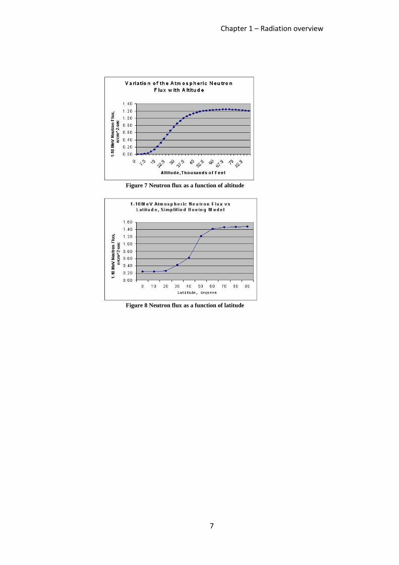
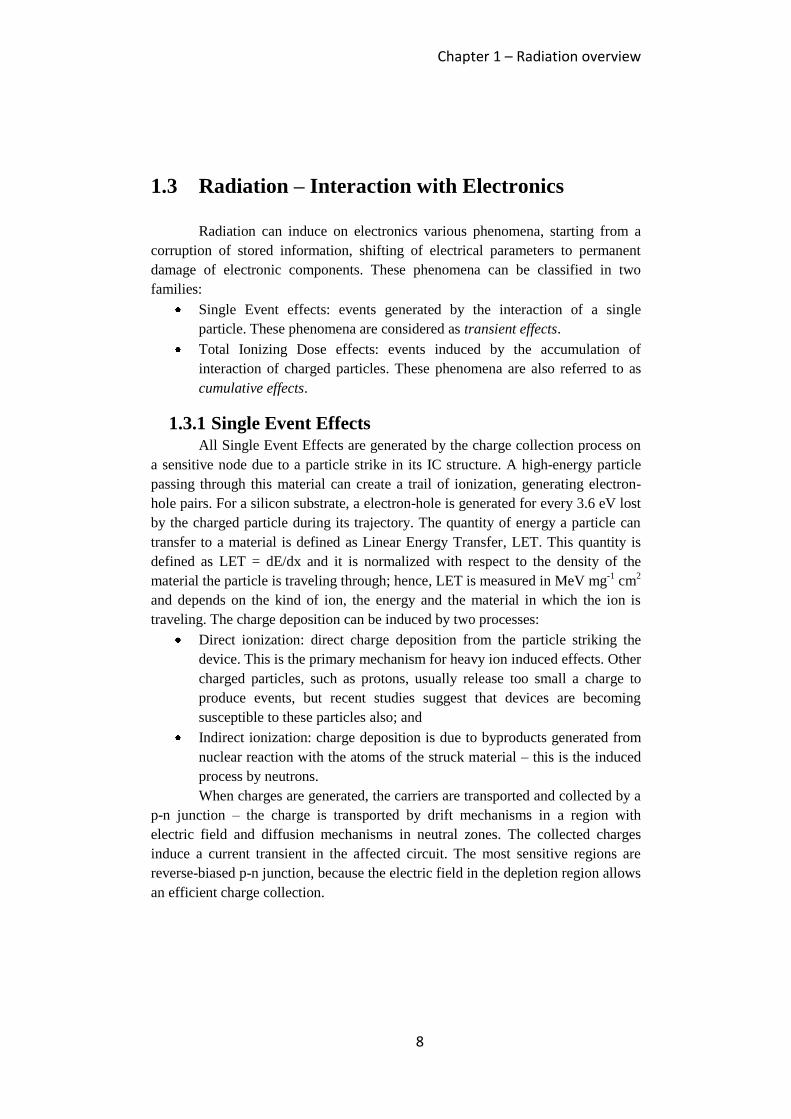
flux varies with altitude, as shown in Figure 7, where the peak is at 60,000 feet and
at Earth’s surface, the neutron flux is about 1/500 of the flux peak. Varying with
latitude, the flux increment moving in the pole direction (Figure 8). Furthermore,
there is also dependency on longitude and solar cycle activity. Notably, in solar
minimum period, the quantity of GCR reaching the Earth increases. The reference
Chapter 1 – Radiation overview
6
neutron flux is considered the flux in New York City, where on average there are
13 neutrons per square centimeter per hour (JEDEC, 2006). Recent measurements
of neutron flux at ground level are presented in literature (Gordon, et al., 2004) and
the results are compared with the JEDEC model.
Neutrons are classified by their energy:
Thermal neutrons have energy levels less than 1eV; and
Fast neutrons have energy levels above 100 keV.
Generally, thermal neutrons induce no problems in electronic devices, but
if the integrated circuit has 10
Boron4 the sensitivity to this low energy particle
increases. Problems arise from 10
B that is unstable when exposed to neutrons,
breaking into ionizing fragments shortly after absorbing a neutron. The thermal
neutron capture cross-section of 10
B is extremely high in comparison to most other
isotopes present in semiconductor materials – by three to seven orders of
magnitude (Baumann, et al., 2000). The capture of a neutron produces a 7Li recoil
nucleus and an alpha particle and these particles are capable of inducing errors in
electronic devices.
Another problem for terrestrial electronics comes from impurities in
packaging materials (Baumann, 2005). Indeed, manufacturing materials (also
material involved in silicon use) can present radioactive impurities, providing a
source for alpha particles. Accurate screening can reduce this problem, but no
methodologies to eliminate impurities exist. In addition, sensitivity of electronics to
alpha particles is increasing with technological evolution.
4 Typically, Boron 10 was used as a p-dopant in Silicon.
Chapter 1 – Radiation overview
7
Figure 7 Neutron flux as a function of altitude
Figure 8 Neutron flux as a function of latitude
Chapter 1 – Radiation overview
8
1.3 Radiation – Interaction with Electronics
Radiation can induce on electronics various phenomena, starting from a
corruption of stored information, shifting of electrical parameters to permanent
damage of electronic components. These phenomena can be classified in two
families:
Single Event effects: events generated by the interaction of a single
particle. These phenomena are considered as transient effects.
Total Ionizing Dose effects: events induced by the accumulation of
interaction of charged particles. These phenomena are also referred to as
cumulative effects.
1.3.1 Single Event Effects All Single Event Effects are generated by the charge collection process on
a sensitive node due to a particle strike in its IC structure. A high-energy particle
passing through this material can create a trail of ionization, generating electron-
hole pairs. For a silicon substrate, a electron-hole is generated for every 3.6 eV lost
by the charged particle during its trajectory. The quantity of energy a particle can
transfer to a material is defined as Linear Energy Transfer, LET. This quantity is
defined as LET = dE/dx and it is normalized with respect to the density of the
material the particle is traveling through; hence, LET is measured in MeV mg-1
cm2
and depends on the kind of ion, the energy and the material in which the ion is
traveling. The charge deposition can be induced by two processes:
Direct ionization: direct charge deposition from the particle striking the
device. This is the primary mechanism for heavy ion induced effects. Other
charged particles, such as protons, usually release too small a charge to
produce events, but recent studies suggest that devices are becoming
susceptible to these particles also; and
Indirect ionization: charge deposition is due to byproducts generated from
nuclear reaction with the atoms of the struck material – this is the induced
process by neutrons.
When charges are generated, the carriers are transported and collected by a
p-n junction – the charge is transported by drift mechanisms in a region with
electric field and diffusion mechanisms in neutral zones. The collected charges
induce a current transient in the affected circuit. The most sensitive regions are
reverse-biased p-n junction, because the electric field in the depletion region allows
an efficient charge collection.
Chapter 1 – Radiation overview
9
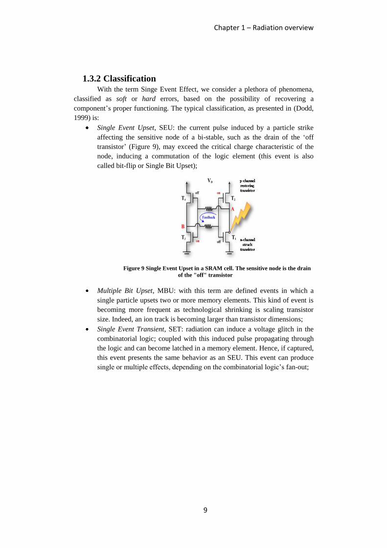
1.3.2 Classification With the term Singe Event Effect, we consider a plethora of phenomena,
classified as soft or hard errors, based on the possibility of recovering a
component’s proper functioning. The typical classification, as presented in (Dodd,
1999) is:
Single Event Upset, SEU: the current pulse induced by a particle strike
affecting the sensitive node of a bi-stable, such as the drain of the ‘off
transistor’ (Figure 9), may exceed the critical charge characteristic of the
node, inducing a commutation of the logic element (this event is also
called bit-flip or Single Bit Upset);
Figure 9 Single Event Upset in a SRAM cell. The sensitive node is the drain
of the "off" transistor
Multiple Bit Upset, MBU: with this term are defined events in which a
single particle upsets two or more memory elements. This kind of event is
becoming more frequent as technological shrinking is scaling transistor
size. Indeed, an ion track is becoming larger than transistor dimensions;
Single Event Transient, SET: radiation can induce a voltage glitch in the
combinatorial logic; coupled with this induced pulse propagating through
the logic and can become latched in a memory element. Hence, if captured,
this event presents the same behavior as an SEU. This event can produce
single or multiple effects, depending on the combinatorial logic’s fan-out;
Chapter 1 – Radiation overview
10
Figure 10 Single Event Transient. A radiation-induced voltage glitch affecting
combinatorial logic, can propagate through the logic and become latched by a memory element
Single Event Latchup, SEL: this event is considered a hard error. The
energy released by a particle strike can activate the parasitic thyristor
embedded in the CMOS architecture. When activated, this structure
presents a positive feedback, causing the involved transistor to start to
drain high current. This event leads to permanent damage; and
Figure 11 Single Event Latchup. Parasitic structure embedded in a CMOS transistor.
Single Event Functional Interrupt, SEFI: this event happens when a
charged particle induces a modification of special registers controlling the
device functionalities, compromising the component’s correct behavior.
1.3.3 Total Ionizing Dose When an MOS structure is exposed to high energy ionizing irradiation,
charges are created in the oxide (Schwank, et al., 2008). A buildup of carriers in
the oxide leads to degradation of transistor behavior (shifting of its electrical
parameters). Recombination after ionization is possible, and any charge escaping
from this process is defined as charge yield. For the hole-electron pairs escaping
from recombination, in a few picoseconds, the majority of electrons drift toward
the gate, while holes drift toward the Si/SiO2 interface. Approaching the Si/SiO2
interface, some holes will be trapped, creating a positive oxide trap charge.
In addition, other insulators – such as buried oxides in SOI structures – can
trap positive charges. This charge trapping can invert the channel interface, causing
leakage currents to flow also when a transistor in the ‘off’ state, hence increasing
the static power consumption. These effects lead to a degradation of that transistor,
modifying the voltage threshold and degrading the timing performance.
Chapter 1 – Radiation overview
11
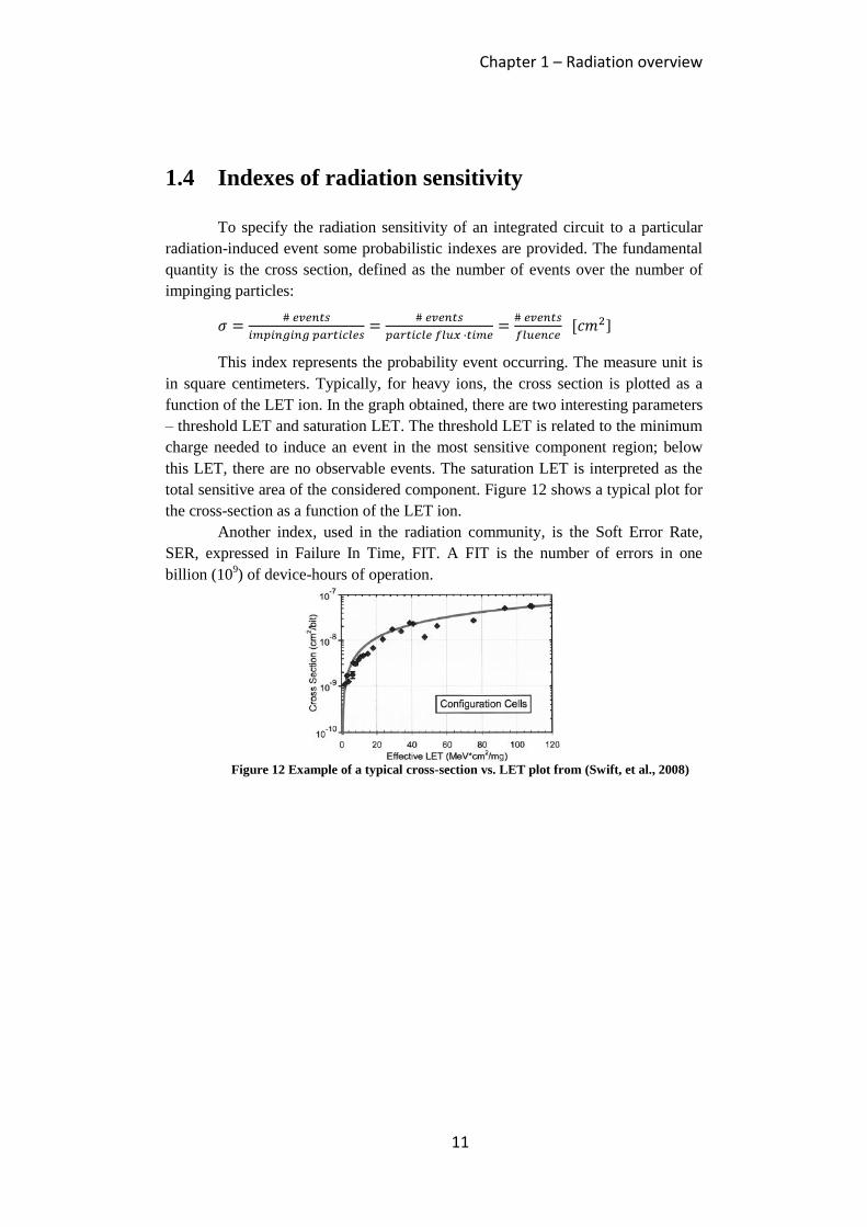
1.4 Indexes of radiation sensitivity
To specify the radiation sensitivity of an integrated circuit to a particular
radiation-induced event some probabilistic indexes are provided. The fundamental
quantity is the cross section, defined as the number of events over the number of
impinging particles:
]
This index represents the probability event occurring. The measure unit is
in square centimeters. Typically, for heavy ions, the cross section is plotted as a
function of the LET ion. In the graph obtained, there are two interesting parameters
– threshold LET and saturation LET. The threshold LET is related to the minimum
charge needed to induce an event in the most sensitive component region; below
this LET, there are no observable events. The saturation LET is interpreted as the
total sensitive area of the considered component. Figure 12 shows a typical plot for
the cross-section as a function of the LET ion.
Another index, used in the radiation community, is the Soft Error Rate,
SER, expressed in Failure In Time, FIT. A FIT is the number of errors in one
billion (109) of device-hours of operation.
Figure 12 Example of a typical cross-section vs. LET plot from (Swift, et al., 2008)

13
Chapter 2
Radiation Effects on SRAM-based
FPGAs
Field Programmable Gate Arrays, FPGAs, are integrated circuits offering
reconfiguration capabilities. Classification of these kinds of devices is based on the
technology used to maintain the information regarding the device configuration. In
this chapter, we focus on FPGA produced by Xilinx, based on Static Random
Access Memory, SRAM. SRAM-based FPGAs are an attractive solution for many
applications where short development time, low-cost for low-production volumes,
and in-the-field-programming ability are important issues. The versatility SRAM-
based FPGAs offer comes from the adoption of a configuration memory whose
content defines the operations of the circuit these FPGA implement. It is therefore
fundamental that the content of the configuration memory maintains the desired
values during the FPGA operation. One of the few major disadvantages of SRAM-
based FPGAs is their sensitivity to ionizing radiation. A change in configuration
memory due to radiation can modify the implemented circuit, possibly leading to
Single Event Functional Interruptions, SEFI. The technological evolution is
exacerbating radiation issues, since more scaled devices are usually more sensitive
to ionizing particles. In particular, technology shrinking is leading to an increasing
occurrence of Multiple Bit Upsets, MBU, which may defy many hardening-by-
design solutions. Our work has focused on Xilinx FPGAs and the results presented
herein come from collaboration with Politecnico di Torino. Analysis of the effects
of neutrons and heavy-ions are reported for Xilinx Spartan-3 devices.
2.1 FPGA Architecture
Basic FPGA structure is composed of an array of Logic Blocks, I/O pads
and configurable interconnections. Logic Blocks can be configured to perform a
combinatorial or sequential logic function. With technology evolution, these logic
blocks are becoming more complex and capable of performing functions that are
Chapter 2 – Radiation Effects on SRAM-Based FPGAs
14
more sophisticated. For example, Figure 13 shows the architecture of a
Configurable Logic Block, CLB in Xilinx Spartan-3 devices. In Xilinx
terminology, this CLB is composed of four slices. A slice is the basic configurable
logic element and each one contains two Look-Up Tables,5 LUTs, to implement
logic and two storage elements that can be used as latches or flip-flop. A LUT can
be used to implement a 16x1 RAM memory element as well as a 16-bit shift
register. Additionally, carry logic and multiplexer are present to optimize the
implementation of arithmetic functions. These four slices are grouped in pairs and
each pair is organized as a column. For example, in the Spartan-3 architecture,
there is a diversification in the columns capabilities – right pairs support only logic,
while left pairs can also implement memory (shift register and RAM).
Interface with the external world is obtained by means of input/output
configurable blocks. I/Os can be configured to comply with different standards,
current values, voltages, buffering or terminations. In these blocks, Double Data
Rate, DDR, registers and input delay lines are also included to allow memory
interfacing and to provide functionalities that are more complex.
5 Every LUT in a Xilinx Spartan-3 device can provide a 4-inputs 1-output logic
function and can be combined to provide more complex functions.
Figure 13 Xilinx Spartan-3
Configurable Logic Block (source Xilinx
Spartan-3 User Guide)
Chapter 2 – Radiation Effects on SRAM-Based FPGAs
15
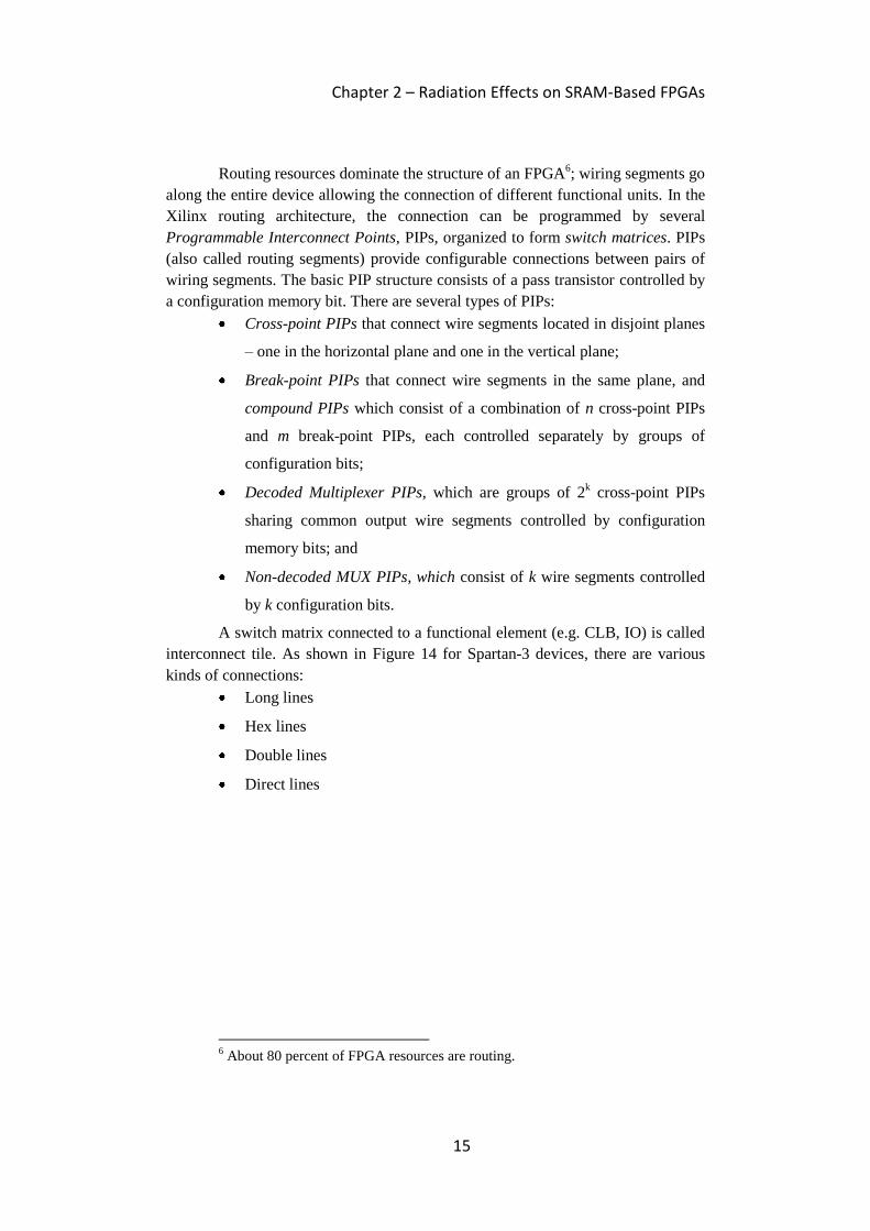
Routing resources dominate the structure of an FPGA6; wiring segments go
along the entire device allowing the connection of different functional units. In the
Xilinx routing architecture, the connection can be programmed by several
Programmable Interconnect Points, PIPs, organized to form switch matrices. PIPs
(also called routing segments) provide configurable connections between pairs of
wiring segments. The basic PIP structure consists of a pass transistor controlled by
a configuration memory bit. There are several types of PIPs:
Cross-point PIPs that connect wire segments located in disjoint planes
– one in the horizontal plane and one in the vertical plane;
Break-point PIPs that connect wire segments in the same plane, and
compound PIPs which consist of a combination of n cross-point PIPs
and m break-point PIPs, each controlled separately by groups of
configuration bits;
Decoded Multiplexer PIPs, which are groups of 2k cross-point PIPs
sharing common output wire segments controlled by configuration
memory bits; and
Non-decoded MUX PIPs, which consist of k wire segments controlled
by k configuration bits.
A switch matrix connected to a functional element (e.g. CLB, IO) is called
interconnect tile. As shown in Figure 14 for Spartan-3 devices, there are various
kinds of connections:
Long lines
Hex lines
Double lines
Direct lines
6 About 80 percent of FPGA resources are routing.
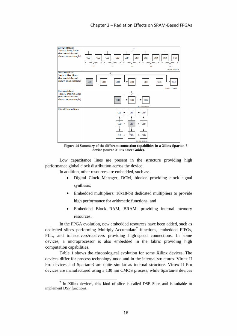
Chapter 2 – Radiation Effects on SRAM-Based FPGAs
16
Figure 14 Summary of the different connection capabilities in a Xilinx Spartan-3
device (source Xilinx User Guide).
Low capacitance lines are present in the structure providing high
performance global clock distribution across the device.
In addition, other resources are embedded, such as:
Digital Clock Manager, DCM, blocks: providing clock signal
synthesis;
Embedded multipliers: 18x18-bit dedicated multipliers to provide
high performance for arithmetic functions; and
Embedded Block RAM, BRAM: providing internal memory
resources.
In the FPGA evolution, new embedded resources have been added, such as
dedicated slices performing Multiply-Accumulate7 functions, embedded FIFOs,
PLL, and transceivers/receivers providing high-speed connections. In some
devices, a microprocessor is also embedded in the fabric providing high
computation capabilities.
Table 1 shows the chronological evolution for some Xilinx devices. The
devices differ for process technology node and in the internal structures. Virtex II
Pro devices and Spartan-3 are quite similar as internal structure. Virtex II Pro
devices are manufactured using a 130 nm CMOS process, while Spartan-3 devices
7 In Xilinx devices, this kind of slice is called DSP Slice and is suitable to
implement DSP functions.
Chapter 2 – Radiation Effects on SRAM-Based FPGAs
17
require a 90 nm process. With the introduction of Virtex-4 devices, Xilinx added
the DSP slices. This kind of slice provides 18x18 bit dedicated multipliers, adder
and 48 bit accumulator to optimize signal processing function implementation. In
addition, their embedded block RAM has been improved to implement high
performance FIFOs with different read/write clocks, along with implementation of
architecture evolution improvements in their routing structures as well as in clock
distribution.
Virtex-5 devices have introduced new LUT structures providing 6 inputs 1
output. In addition, their CLB organization has changed. In these devices, a logic
block is composed of two slices, and every slice has four LUTs, four memory
elements, multiplexers and carry logic.
Device Family
Manufacturing
Technology
[nm]
CFM Technology
[nm]
Virtex-II Pro 130 130
Spartan-3 90 90
Virtex-4 90 130
Virtex-5 65 90
Table 1 Xilinx architecture improvements. Technology process employed by some
different Xilinx FPGAs. In particular, in some families, the process used for the configuration
memory, CFM, differs from that used for logic.
2.2 FPGA Configuration
High-level description languages8 are used to describe the circuit the
FPGA has to implement. A vendor’s tools will produce at the end of their
development process a configuration file for their device. All internal resources are
configured downloading the content of this file into the configuration memory.
This process is called ‘configuration’ and the configuration file is called bitstream.
A state machine, embedded in the device, will take care of its configuration
memory operations. A reverse process, the reading of the configuration memory, is
called readback. The Xilinx FPGAs present various protocols to handle the
configuration memory (Xilinx, UG332). In particular, in our work, we used the
Join Test Action Group, JTAG, standard IEEE 1149.1. Due to the nature of the
configuration memory, at power-up, the device is unconfigured and a non-volatile
memory has to provide its configuration bitstream. In the development process, the
bitstream can be downloaded with a dedicated programming device.
8 Such as VHDL, Verilog, SystemC, and similar.
Chapter 2 – Radiation Effects on SRAM-Based FPGAs
18
2.3 SEE in SRAM-based FPGA
Unfortunately, the SRAM technology, in which the configuration memory
is based, has proved to be quite sensitive to radiation-induced effects. All the
above-mentioned resources are controlled by the configuration memory, which is a
set of storage elements – implemented using SRAM technology9 – placed inside
the FPGA device. Configuration memory content defines how wiring segments,
logic blocks, and switch boxes are used for implementing a given circuit. A soft
error affecting such a memory may have a dramatic impact, since it may change a
circuit’s operating. Although they induce no permanent modifications to the
hardware, when soft errors occur in the FPGA configuration memory they may
alter the implemented circuit, until new configuration data is written. Errors
produced by soft errors in an FPGA configuration memory – Single Event Upset,
SEU – can be classified in two different categories – errors affecting logic blocks
and errors affecting routing resources (Sterpone, et al., 2006).
As far as logic-block errors are concerned, several different phenomena
may be observed, depending on which logic block resource was modified by a
SEU:
1. LUT error: the SEU modified one bit of a LUT, thus changing the
combinational function it implements.
2. MUX error: the SEU modified the configuration of a MUX in the
logic block; as a result, signals are incorrectly forwarded inside the
logic block.
3. FF error: the SEU modified the configuration of a FF, for example
changing the polarity of the reset line, or that of the clock line.
As far as switch boxes are concerned, different phenomena are possible.
Although a SEU affecting a switch box modifies the configuration of only one PIP,
both single and multiple effects can be originated.
Single effects happen when any modifications induced by an SEU only
alter the affected PIP. In this case, one situation may happen, which we call open –
the SEU changes the configuration of the affected PIP in such a way that the
existing connection between two routing segments is opened.
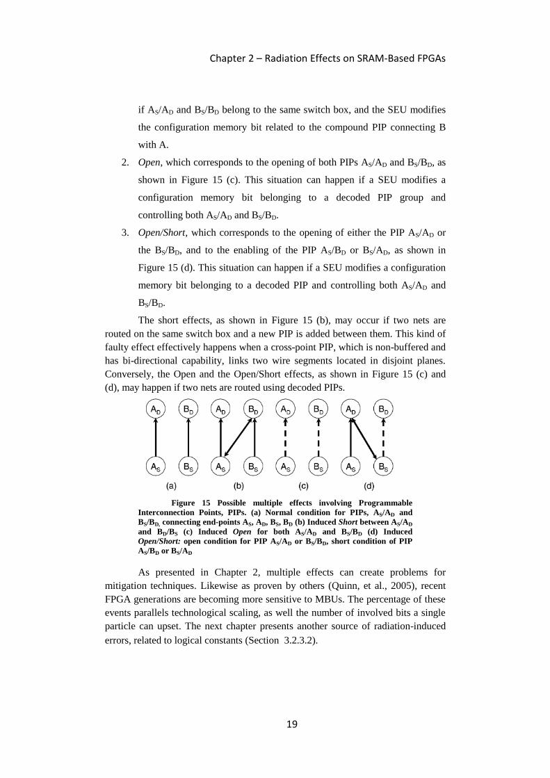
In order to describe the multiple effects, let us consider two PIPs AS/AD
and BS/BD connecting the end-points AS, AD, BS, BD as shown in Figure 15 (a). We
identified the following modifications that could be introduced by a SEU.
1. Short between AS/AD and BD/BS. As shown in Figure 15 (b), a third PIP
connecting either one end of A to one end of B is enabled. This can happen
9 Xilinx for the configuration memory implements a 5-transistor cell.
Chapter 2 – Radiation Effects on SRAM-Based FPGAs
19
if AS/AD and BS/BD belong to the same switch box, and the SEU modifies
the configuration memory bit related to the compound PIP connecting B
with A.
2. Open, which corresponds to the opening of both PIPs AS/AD and BS/BD, as
shown in Figure 15 (c). This situation can happen if a SEU modifies a
configuration memory bit belonging to a decoded PIP group and
controlling both AS/AD and BS/BD.
3. Open/Short, which corresponds to the opening of either the PIP AS/AD or
the BS/BD, and to the enabling of the PIP AS/BD or BS/AD, as shown in
Figure 15 (d). This situation can happen if a SEU modifies a configuration
memory bit belonging to a decoded PIP and controlling both AS/AD and
BS/BD.
The short effects, as shown in Figure 15 (b), may occur if two nets are
routed on the same switch box and a new PIP is added between them. This kind of
faulty effect effectively happens when a cross-point PIP, which is non-buffered and
has bi-directional capability, links two wire segments located in disjoint planes.
Conversely, the Open and the Open/Short effects, as shown in Figure 15 (c) and
(d), may happen if two nets are routed using decoded PIPs.
Figure 15 Possible multiple effects involving Programmable
Interconnection Points, PIPs. (a) Normal condition for PIPs, AS/AD and
BS/BD, connecting end-points AS, AD, BS, BD (b) Induced Short between AS/AD
and BD/BS (c) Induced Open for both AS/AD and BS/BD (d) Induced
Open/Short: open condition for PIP AS/AD or BS/BD, short condition of PIP
AS/BD or BS/AD
As presented in Chapter 2, multiple effects can create problems for
mitigation techniques. Likewise as proven by others (Quinn, et al., 2005), recent
FPGA generations are becoming more sensitive to MBUs. The percentage of these
events parallels technological scaling, as well the number of involved bits a single
particle can upset. The next chapter presents another source of radiation-induced
errors, related to logical constants (Section 3.2.3.2).
Chapter 2 – Radiation Effects on SRAM-Based FPGAs
20
Radiation effects involving configuration circuitry can also lead to SEFI.
Typical SEFI conditions for a FPGA are as found in literature (Yui, et al., 2003):
Power on Reset, POR, SEFI: this event induces a reset of the FPGA, losing
configuration memory content and the device’s state. In this case, that
device has to be reconfigured. This condition can be detected as a drop in
the device’s power consumption and a variation of the Done pin; and
SelectMap/JTAG SEFI: this event leads to problems in the configuration
interface. A device is unresponsive to configuration commands such as
readback. JTAG interface sensitivity typically is very low (Swift, 2004).
2.4 Radiation sensitivity: test methodologies
Different methods exist to assess the radiation sensitivity of a device (or a
particular implemented design) to radiation effects. Radiation effects can be
studied (for the terrestrial environment) with life testing. An example of this
methodology is represented by the Xilinx Rosetta Experiment (Lesea, et al., 2005).
Large arrays of FPGAs were placed in different locations at different altitudes10
.
This testing technique provides sensitivity data in the real environment, but
unfortunately, it needs a long time to collect statistical data – months to years – and
involves a large number of devices11
. Another approach is accelerated testing,
where, particle accelerators or radiation sources are used to simulate the device’s
final radiation-environment, but with an accelerated factor. In this way, a short
time is required to collect data and experiments are easily repeatable. In addition,
this approach presents some drawbacks. For example, irradiation is anisotropic, as
in the real case, and for outer space environment; and it is impossible to reproduce
the high energy of some particles.
At design level, an interesting technique for analyzing induced error
impacts in an FPGA implemented circuit is the fault injection method (Alderighi,
et al., 2003), (Lima, et al., 2001). The basic principle of this method is configuring
an FPGA with a corrupted bitstream, emulating a radiation-induced error. This
methodology has the advantage that it needs no radiation source to analyze the
consequence of errors in the configuration memory on the design’s operation. Fault
injection discovers the sensitive configuration bit for a design and can verify the
effectiveness of implemented hardening techniques.
10
Altitude is the only accelerator factor for these kinds of tests. 11
Furthermore, devices need to be in production, and the required time to obtain
data in the developing process is incompatible with the market time demand.

Chapter 2 – Radiation Effects on SRAM-Based FPGAs
21
2.5 Radiation Tests
In the following sections, radiation tests are presented. Throughout the
experiments, we used commercial SRAM-based FPGAs manufactured by Xilinx.
In particular, we irradiated and studied Xilinx Spartan-3 XC3S200. (Xilinx,
UG331) This device is manufactured using a 90 nm CMOS technology and
features 4,320 logic cells, 141 user I/Os and a bitstream size of 1,043,040 bits. We
irradiated with a variety radiation sources:
Neutrons
Alpha particles
Heavy-ions
X-rays
Before heavy-ion, alpha, and X-ray irradiation, the plastic package was
etched with a nitric acid attack to expose completely the component die to radiation
sources (Figure 16).
2.5.1 Neutron Experiment We performed a set of radiation testing experiments at the ISIS neutron
facility12
, using the VESUVIO instrument. We created a test platform to control
these experiments and to analyze any detected events. This methodology once
adopted can be used to assess radiation sensitivity of a device as well the sensitivity
of an implemented design. Our samples had no need for special preparation
because the plastic packaging presents no problems for neutrons to reach the device
active area. Indeed, a concrete wall two meters thick is needed to stop high-energy
neutrons.
12
ISIS website: http://www.isis.rl.ac.uk
Figure 16 Device Under Test:
decapsulated Xilinx Spartan-3 XC3S200

Chapter 2 – Radiation Effects on SRAM-Based FPGAs
22
2.5.1.1 ISIS Neutron source
The ISIS neutron source is located at the CCLRC Rutherford Appleton
Laboratory, Didcot, U.K., and has been used so far for condensed matter studies.
Neutrons are produced at ISIS by the spallation process (Watanabe, 2003): a
heavy-metal target (tungsten) is bombarded with pulses of highly energetic
protons, generating neutrons from the nuclei of the target atoms. The acceleration
process is composed of two steps – first, ions are injected into a linear accelerator,
LINAC. The beam is converted to protons by a 0.3 µm thick aluminum oxide
stripping foil and then accelerated in a synchrotron. High-energy proton pulses
finally strike the tungsten target and corresponding pulses of neutrons are freed by
spallation. The energy of the produced neutrons is reduced through a moderator,
which can be of different types. The resulting neutron beam reaches 26 different
lines (Figure 18), including the VESUVIO line where our experiments were
performed. VESUVIO is commonly employed for condensed matter studies,
exploiting neutrons above 1 eV, the so-called epithermal neutrons. The sample S is
located at a distance L0=11,055 m from the water moderator. The aluminum sample
tank is of cylindrical form, with an internal diameter of 50 cm (Figure 19). The
height is 65 cm and the beam center is located at about 30 cm from the top. The
spectrum in the high-energy region has been measured through the threshold
activation target technique (Peurrung, 2000). The ISIS spectrum is illustrated in
Figure 17, where it is compared with two of the most widely used neutron sources
(LANSCE and TRIUMF) and with the terrestrial flux multiplied by a factor of 107
and 108. As seen, the ISIS spectrum features a 1/E
α characteristic, with α larger
than one, and provides a flux similar to the terrestrial one with acceleration
Figure 17 ISIS Differential spectrum. Showing
differential neutron flux [n/cm2/s/MeV] as a function of
energy [MeV]. This plot represents data for ISIS and
another two neutron facilities – LANSCE and TRIUF. The
dotted line represents neutron flux at sea level multiplied by
108.
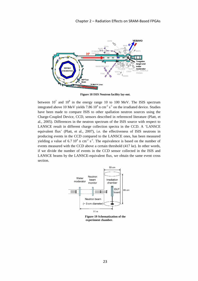
Chapter 2 – Radiation Effects on SRAM-Based FPGAs
23
between 107 and 10
8 in the energy range 10 to 100 MeV. The ISIS spectrum
integrated above 10 MeV yields 7.86 104 n cm
-2 s
-1 on the irradiated device. Studies
have been made to compare ISIS to other spallation neutron sources using the
Charge-Coupled Device, CCD, sensors described in referenced literature (Platt, et
al., 2005). Differences in the neutron spectrum of the ISIS source with respect to
LANSCE result in different charge collection spectra in the CCD. A ‘LANSCE
equivalent flux’ (Platt, et al., 2007), i.e. the effectiveness of ISIS neutrons in
producing events in the CCD compared to the LANSCE ones, has been measured
yielding a value of 6.7 104 n cm
-2 s
-1. The equivalence is based on the number of
events measured with the CCD above a certain threshold (417 ke). In other words,
if we divide the number of events in the CCD sensor collected in the ISIS and
LANSCE beams by the LANSCE-equivalent flux, we obtain the same event cross
section.
Figure 18 ISIS Neutron facility lay-out.
Figure 19 Schematization of the
experiment chamber.
Chapter 2 – Radiation Effects on SRAM-Based FPGAs
24
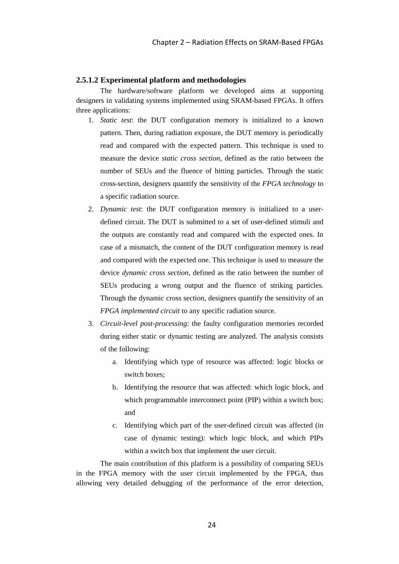
2.5.1.2 Experimental platform and methodologies
The hardware/software platform we developed aims at supporting
designers in validating systems implemented using SRAM-based FPGAs. It offers
three applications:
1. Static test: the DUT configuration memory is initialized to a known
pattern. Then, during radiation exposure, the DUT memory is periodically
read and compared with the expected pattern. This technique is used to
measure the device static cross section, defined as the ratio between the
number of SEUs and the fluence of hitting particles. Through the static
cross-section, designers quantify the sensitivity of the FPGA technology to
a specific radiation source.
2. Dynamic test: the DUT configuration memory is initialized to a user-
defined circuit. The DUT is submitted to a set of user-defined stimuli and
the outputs are constantly read and compared with the expected ones. In
case of a mismatch, the content of the DUT configuration memory is read
and compared with the expected one. This technique is used to measure the
device dynamic cross section, defined as the ratio between the number of
SEUs producing a wrong output and the fluence of striking particles.
Through the dynamic cross section, designers quantify the sensitivity of an
FPGA implemented circuit to any specific radiation source.
3. Circuit-level post-processing: the faulty configuration memories recorded
during either static or dynamic testing are analyzed. The analysis consists
of the following:
a. Identifying which type of resource was affected: logic blocks or
switch boxes;
b. Identifying the resource that was affected: which logic block, and
which programmable interconnect point (PIP) within a switch box;
and
c. Identifying which part of the user-defined circuit was affected (in
case of dynamic testing): which logic block, and which PIPs
within a switch box that implement the user circuit.
The main contribution of this platform is a possibility of comparing SEUs
in the FPGA memory with the user circuit implemented by the FPGA, thus
allowing very detailed debugging of the performance of the error detection,
Chapter 2 – Radiation Effects on SRAM-Based FPGAs
25
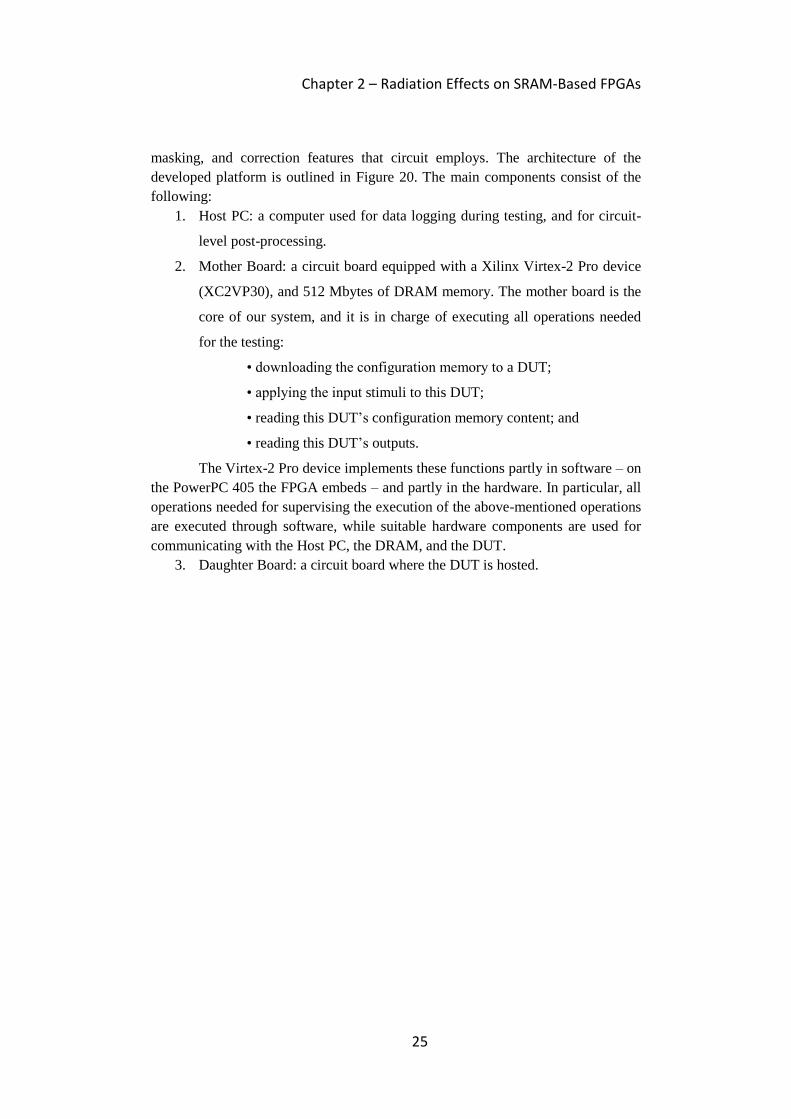
masking, and correction features that circuit employs. The architecture of the
developed platform is outlined in Figure 20. The main components consist of the
following:
1. Host PC: a computer used for data logging during testing, and for circuit-
level post-processing.
2. Mother Board: a circuit board equipped with a Xilinx Virtex-2 Pro device
(XC2VP30), and 512 Mbytes of DRAM memory. The mother board is the
core of our system, and it is in charge of executing all operations needed
for the testing:
• downloading the configuration memory to a DUT;
• applying the input stimuli to this DUT;
• reading this DUT’s configuration memory content; and
• reading this DUT’s outputs.
The Virtex-2 Pro device implements these functions partly in software – on
the PowerPC 405 the FPGA embeds – and partly in the hardware. In particular, all
operations needed for supervising the execution of the above-mentioned operations
are executed through software, while suitable hardware components are used for
communicating with the Host PC, the DRAM, and the DUT.
3. Daughter Board: a circuit board where the DUT is hosted.

Chapter 2 – Radiation Effects on SRAM-Based FPGAs
26
2.5.1.3 Test procedures
Figure 21 resumes the experimental steps for the static test. The Mother
Board configured the DUT, and then we started its neutron irradiation. After
irradiating for a certain amount of time, we stopped the beam and we issued a
readback command to the control platform. Then, we reconfigured the FPGA under
test, and we repeated the experiment’s steps. All the gathered readback bitstreams
were stored in the Host PC for post processing.
FPGA
configuration
Start irradiation –
Neutron beam on
Stop irradiation –
Neutron beam off
FPGA readback
Irradiation
Figure 21 Procedure for the static test for neutron irradiation experiments.
Figure 20 Developed neutron test platform
schematic.

Chapter 2 – Radiation Effects on SRAM-Based FPGAs
27
For the dynamic test, we configured the FPGA under test before starting
irradiation. The readback process was triggered by both a mismatch in the expected
outputs and the expiration of a programmed time. In case of a mismatch between
the golden unit and the actual DUT’s outputs, a reconfiguration operation followed
by a circuit reset was planned. The readback operations at fixed interval times have
been used to analyze, with post-processing, the build-up of faulty conditions in the
tested circuit. The flow chart in Figure 22 summarizes the dynamic test procedure.
FPGA
configuration &
design reset
Beam On
Output
mismatch?Yes FPGA readback
FPGA
reconfiguration
and design reset
Is the interval
time elapsed?
No
Neutron Irradiation
Yes
No
Figure 22 Procedure for the dynamic test for neutron irradiation experiments.
2.5.1.4 CILANTO – circuit post processing
Circuit-level post-processing consists in analyzing the content of the FPGA
configuration memory collected during radiation testing and in identifying the
modifications induced by SEUs to the resources of the FPGA. These analyses are
performed through the CIrcuit-Level ANalysis TOol, CILANTO (Bellato, et al.,
2006), which exploits a database where the relationship between the FPGA
resources and the configuration memory bits is described.
Decoding of the configuration memory has been obtained considering for
every resource their related configuration bits, modifying the resource
configuration and recording the introduced bitstream modification. In Xilinx
devices, the entire FPGA configuration description is stored in a proprietary Native
Circuit Description file, NCD. This file is in a closed format and it is neither
editable nor readable, but it is possible to convert this file into a XDL file. This file
is a text representation in a human readable language of the configuration
information coded in the NCD file. This file reports the FPGA internal
Chapter 2 – Radiation Effects on SRAM-Based FPGAs
28
configuration at a very low-level; it can be edited and further reconverted into a
NCD file. The Xilinx tools operating with the circuit description files are:
a NCD2XDL generates a low-level description of the circuit mapped onto a
device and allows the modification of its internal resources’ configuration;
an XDL2NCD executes the inverse operation, generating a NCD file starting
from a XDL file; and
a BITGEN tool converts a NCD file into a configuration bitstream.
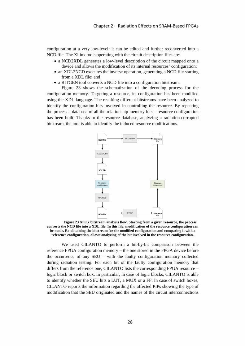
Figure 23 shows the schematization of the decoding process for the
configuration memory. Targeting a resource, its configuration has been modified
using the XDL language. The resulting different bitstreams have been analyzed to
identify the configuration bits involved in controlling the resource. By repeating
the process a database of all the relationship memory bits – resource configuration
has been built. Thanks to the resource database, analyzing a radiation-corrupted
bitstream, the tool is able to identify the induced resource modifications.
BITGEN tool
NCD2XDL tool
Resource
modification
XDL2NCD
BITGEN
Bitstream
comparison
NCD fileBitstream
file
XDL file
NCD fileBitstream
file
Figure 23 Xilinx bitstream analysis flow. Starting from a given resource, the process
converts the NCD file into a XDL file. In this file, modification of the resource configuration can
be made. Re-obtaining the bitstream for the modified configuration and comparing it with a
reference configuration, allows analyzing of the bit involved in the resource configuration.
We used CILANTO to perform a bit-by-bit comparison between the
reference FPGA configuration memory – the one stored in the FPGA device before
the occurrence of any SEU – with the faulty configuration memory collected
during radiation testing. For each bit of the faulty configuration memory that
differs from the reference one, CILANTO lists the corresponding FPGA resource –
logic block or switch box. In particular, in case of logic blocks, CILANTO is able
to identify whether the SEU hits a LUT, a MUX or a FF. In case of switch boxes,
CILANTO reports the information regarding the affected PIPs showing the type of
modification that the SEU originated and the names of the circuit interconnections
Chapter 2 – Radiation Effects on SRAM-Based FPGAs
29
that use the PIPs involved in the modification. CILANTO implements an important
feature that consists of identifying those bits of the FPGA configuration memory
that are sensitive for a given user-circuit the FPGA implements. They include those
bits whose value must be defined for configuring the FPGA resources in such a
way that the FPGA implements the user circuit, and those bits that are unused by
the user circuit, but that may have side effects on the user circuit when altered by
SEUs.
2.5.1.5 Neutron irradiation data
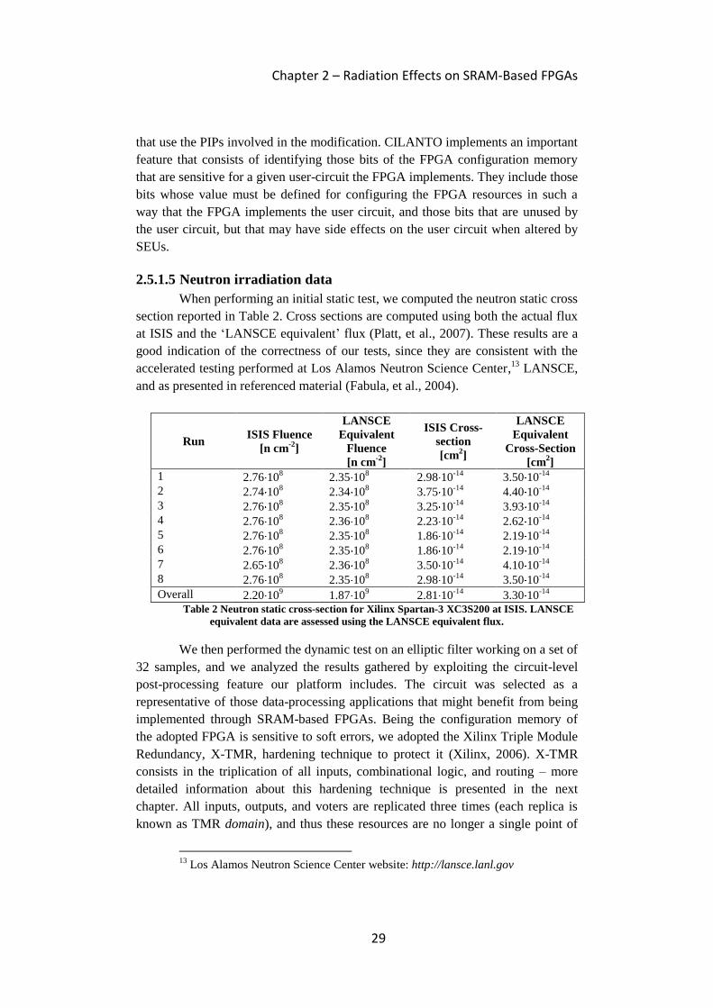
When performing an initial static test, we computed the neutron static cross
section reported in Table 2. Cross sections are computed using both the actual flux
at ISIS and the ‘LANSCE equivalent’ flux (Platt, et al., 2007). These results are a
good indication of the correctness of our tests, since they are consistent with the
accelerated testing performed at Los Alamos Neutron Science Center,13
LANSCE,
and as presented in referenced material (Fabula, et al., 2004).
Run ISIS Fluence
[n cm-2
]
LANSCE
Equivalent
Fluence
[n cm-2
]
ISIS Cross-
section
[cm2]
LANSCE
Equivalent
Cross-Section
[cm2]
1 2.76 108 2.35 10
8 2.98 10
-14 3.50 10
-14
2 2.74 108 2.34 10
8 3.75 10
-14 4.40 10
-14
3 2.76 108 2.35 10
8 3.25 10
-14 3.93 10
-14
4 2.76 108 2.36 10
8 2.23 10
-14 2.62 10
-14
5 2.76 108 2.35 10
8 1.86 10
-14 2.19 10
-14
6 2.76 108 2.35 10
8 1.86 10
-14 2.19 10
-14
7 2.65 108 2.36 10
8 3.50 10
-14 4.10 10
-14
8 2.76 108 2.35 10
8 2.98 10
-14 3.50 10
-14
Overall 2.20 109 1.87 10
9 2.81 10
-14 3.30 10
-14
Table 2 Neutron static cross-section for Xilinx Spartan-3 XC3S200 at ISIS. LANSCE
equivalent data are assessed using the LANSCE equivalent flux.
We then performed the dynamic test on an elliptic filter working on a set of
32 samples, and we analyzed the results gathered by exploiting the circuit-level
post-processing feature our platform includes. The circuit was selected as a
representative of those data-processing applications that might benefit from being
implemented through SRAM-based FPGAs. Being the configuration memory of
the adopted FPGA is sensitive to soft errors, we adopted the Xilinx Triple Module
Redundancy, X-TMR, hardening technique to protect it (Xilinx, 2006). X-TMR
consists in the triplication of all inputs, combinational logic, and routing – more
detailed information about this hardening technique is presented in the next
chapter. All inputs, outputs, and voters are replicated three times (each replica is
known as TMR domain), and thus these resources are no longer a single point of
13
Los Alamos Neutron Science Center website: http://lansce.lanl.gov
Chapter 2 – Radiation Effects on SRAM-Based FPGAs
30
failure, and the result is potentially immune from upsets provoking a single effect
in the voting circuitry. To ensure constant synchronization between redundant state
machines, X-TMR inserts majority voters on all feedback paths. As a result, the
feedback logic for each state machine is a function of the current state of all three
state machines. If a single error induced by a SEU occurs in combinational logic or
in a state machine, one of the replicas of the circuit behaves differently from the
others. For this reason, in absence of radiation-hardened voting circuits (as in the
case of Virtex or Spartan-3 Xilinx families) X-TMR protects voting logic from
SEUs by replicating three times the voters and by adding circuitry that detects the
replica that is behaving differently and disables it by placing its pin in a high-
impedance state while the other two replicas continue to operate correctly and drive
the correct outputs.
We applied CILANTO to the FPGA configuration memory of the elliptic
filter design hardened by the X-TMR tool and it identified 75,016 configuration
memory bits used by the implemented elliptic filter. Secondly, we used CILANTO
on the several faulty FPGA configuration data memory results recorded during the
radiation experiment. For this analysis, CILANTO identified only 19 configuration
memory bits that have been upset during the entire dynamic test and none of these
bit-flips affects the correct functionality of the implemented elliptic filter. In
particular, we observed that among the 19 bit-flips, 17 are related to configuration
memory bits that control resources unused by the implemented circuit, while only
two bit-flips are related to resources that effectively map the elliptic filter
functionality. The report produced by CILANTO identifies that the effects are
related to interconnection PIPs of a unique TMR domain. In particular, CILANTO
identifies two short effects related to elliptic filter nets belonging only to the
second domain of the TMR; thus they cause no corruption of the TMR circuit
functioning.
2.5.1 Heavy-ion irradiation Heavy-ion irradiation was performed with LET ranging from 3.67 to 61.8
MeV mg-1
cm-2
at the SIRAD14
Facility at the INFN National Laboratory of
Legnaro, Italy. Alpha particles were obtained from a portable americium (241
Am)
source. Our experimental setup consists of a DUT board and a control board. The
control board monitors the FPGA under test, performing readback and
configuration at high speed through the JTAG interface (IEEE Standard 1149.1).
Different configuration bitstreams, corresponding to actual designs, and an empty
bitstream were used during irradiation, to evaluate the dependence on the loaded
pattern.
At first, we analyzed the irradiation results of the XC3S200. The bitstream
has been fully decoded as far as CLBs are concerned, and a mask mapping the
14
Silicon Detector Laboratory, SIRAD, website: http://sirad.pd.infmn.it
Chapter 2 – Radiation Effects on SRAM-Based FPGAs
31
configuration bits to the controlled resources has been obtained by analyzing the
bitstream. Therefore, we can map the radiation-induced bit-flip to the controlled
resource.
2.5.1.1 Static cross-section
The heavy ion cross-section (σ static) for the configuration memory bits
controlling the CLBs is reported in Figure 24 as a function of the ion LET. These
numbers average the contributions of the different CLB resources: Configuration
bits, CONF, Look-up tables, LUT, Multiplexers, MUX, Programmable
Interconnection Points, PIP; which can be both decoded, DPIP and non-decoded,
NPIP.
By analyzing the bitstreams corrupted by the radiation, we can report the
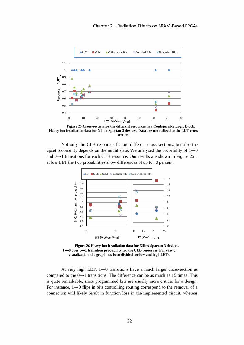
sensitivity of each resource normalized to the LUT cross section Figure 25.
Interestingly enough, each resource has a different cross section, bits controlling
LUTs being the most sensitive ones. MUX, PIPs, CONF bits have a cross-section,
which is about 20 percent smaller than LUTs, and this difference tends to increase
at high LET, greater than 50 MeV cm-2
mg-1
.
1.00E-11
1.00E-10
1.00E-09
1.00E-08
1.00E-07
0 20 40 60 80
Cro
ss-s
ecti
on
per
bit
[cm
2/b
it]
LET [MeV·cm²/mg]
Figure 24 Configurable Logic Block, CLB, cross-section per bit
vs. LET. Heavy-ion irradiation data for Xilinx Spartan-3 devices. The
lower LET point is obtained with alpha particle irradiation. These data
average the contribution of all the CLB resources.
Chapter 2 – Radiation Effects on SRAM-Based FPGAs
32
Figure 25 Cross-section for the different resources in a Configurable Logic Block.
Heavy-ion irradiation data for Xilinx Spartan-3 devices. Data are normalized to the LUT cross
section.
Not only the CLB resources feature different cross sections, but also the
upset probability depends on the initial state. We analyzed the probability of 1→0
and 0→1 transitions for each CLB resource. Our results are shown in Figure 26 –
at low LET the two probabilities show differences of up to 40 percent.
At very high LET, 1→0 transitions have a much larger cross-section as
compared to the 0→1 transitions. The difference can be as much as 15 times. This
is quite remarkable, since programmed bits are usually more critical for a design.
For instance, 1→0 flips in bits controlling routing correspond to the removal of a
connection will likely result in function loss in the implemented circuit, whereas
0.4
0.5
0.6
0.7
0.8
0.9
1
1.1
0 10 20 30 40 50 60 70 80
Re
sou
rce
/
LUT
LET [MeV·cm²/mg]
LUT MUX Cofiguration Bits Decoded PIPs Ndecoded PIPs
0.5
0.6
0.7
0.8
0.9
1
1.1
1.2
1.3
1.4
1.5
3 8
1->0
/ 0-
>1 t
ran
siti
on
pro
bab
ility
LET [MeV·cm²/mg]
0
2
4
6
8
10
12
14
16
60 65 70 75
LET [MeV·cm²/mg]
3 5 7 9
1->0
/ 0-
>1 tr
ansi
tion
prob
abili
ty
LET [MeV·cm²/mg]
LUT MUX CONF. Decoded PIPs Non-Decoded PIPs
Figure 26 Heavy-ion irradiation data for Xilinx Spartan-3 devices.
1 0 over 0 1 transition probability for the CLB resources. For ease of
visualization, the graph has been divided for low and high LETs.
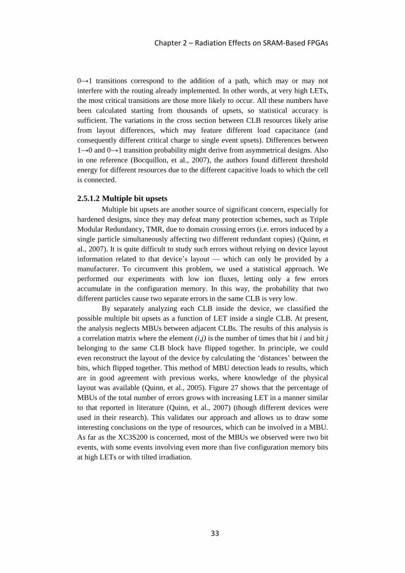
Chapter 2 – Radiation Effects on SRAM-Based FPGAs
33
0→1 transitions correspond to the addition of a path, which may or may not
interfere with the routing already implemented. In other words, at very high LETs,
the most critical transitions are those more likely to occur. All these numbers have
been calculated starting from thousands of upsets, so statistical accuracy is
sufficient. The variations in the cross section between CLB resources likely arise
from layout differences, which may feature different load capacitance (and
consequently different critical charge to single event upsets). Differences between
1→0 and 0→1 transition probability might derive from asymmetrical designs. Also
in one reference (Bocquillon, et al., 2007), the authors found different threshold
energy for different resources due to the different capacitive loads to which the cell
is connected.
2.5.1.2 Multiple bit upsets
Multiple bit upsets are another source of significant concern, especially for
hardened designs, since they may defeat many protection schemes, such as Triple
Modular Redundancy, TMR, due to domain crossing errors (i.e. errors induced by a
single particle simultaneously affecting two different redundant copies) (Quinn, et
al., 2007). It is quite difficult to study such errors without relying on device layout
information related to that device’s layout — which can only be provided by a
manufacturer. To circumvent this problem, we used a statistical approach. We
performed our experiments with low ion fluxes, letting only a few errors
accumulate in the configuration memory. In this way, the probability that two
different particles cause two separate errors in the same CLB is very low.
By separately analyzing each CLB inside the device, we classified the
possible multiple bit upsets as a function of LET inside a single CLB. At present,
the analysis neglects MBUs between adjacent CLBs. The results of this analysis is
a correlation matrix where the element (i,j) is the number of times that bit i and bit j
belonging to the same CLB block have flipped together. In principle, we could
even reconstruct the layout of the device by calculating the ‘distances’ between the
bits, which flipped together. This method of MBU detection leads to results, which
are in good agreement with previous works, where knowledge of the physical
layout was available (Quinn, et al., 2005). Figure 27 shows that the percentage of
MBUs of the total number of errors grows with increasing LET in a manner similar
to that reported in literature (Quinn, et al., 2007) (though different devices were
used in their research). This validates our approach and allows us to draw some
interesting conclusions on the type of resources, which can be involved in a MBU.
As far as the XC3S200 is concerned, most of the MBUs we observed were two bit
events, with some events involving even more than five configuration memory bits
at high LETs or with tilted irradiation.
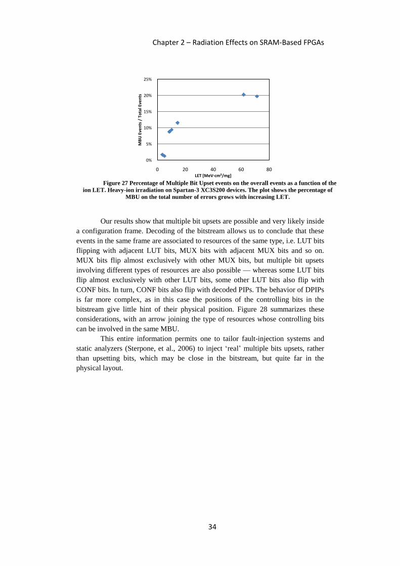
Chapter 2 – Radiation Effects on SRAM-Based FPGAs
34
Figure 27 Percentage of Multiple Bit Upset events on the overall events as a function of the
ion LET. Heavy-ion irradiation on Spartan-3 XC3S200 devices. The plot shows the percentage of
MBU on the total number of errors grows with increasing LET.
Our results show that multiple bit upsets are possible and very likely inside
a configuration frame. Decoding of the bitstream allows us to conclude that these
events in the same frame are associated to resources of the same type, i.e. LUT bits
flipping with adjacent LUT bits, MUX bits with adjacent MUX bits and so on.
MUX bits flip almost exclusively with other MUX bits, but multiple bit upsets
involving different types of resources are also possible — whereas some LUT bits
flip almost exclusively with other LUT bits, some other LUT bits also flip with
CONF bits. In turn, CONF bits also flip with decoded PIPs. The behavior of DPIPs
is far more complex, as in this case the positions of the controlling bits in the
bitstream give little hint of their physical position. Figure 28 summarizes these
considerations, with an arrow joining the type of resources whose controlling bits
can be involved in the same MBU.
This entire information permits one to tailor fault-injection systems and
static analyzers (Sterpone, et al., 2006) to inject ‘real’ multiple bits upsets, rather
than upsetting bits, which may be close in the bitstream, but quite far in the
physical layout.
0%
5%
10%
15%
20%
25%
0 20 40 60 80
MB
U E
ven
ts /
To
tal E
ven
ts
LET [MeV·cm²/mg]

Chapter 2 – Radiation Effects on SRAM-Based FPGAs
35
Figure 28 Possible Multiple Bit Upset events in a configuration memory. An arrow,
between resources A and B means we observed an MBU involving the two resources. The
relationships reflect the resource physical adjacency.
2.5.2 Total Dose and Soft Error Rate To study interactions between Total Ionizing Dose, TID, effects and SEU,
some devices were exposed to X-rays and then the SEU rate was measured with
alpha particles. The accumulated total dose may influence the device error rate.
This was reported in the case of SRAMs (Schwank, et al., 2006), but has never
been studied for FPGAs. To verify this, we exposed our devices to X-rays,
performing a characterization of the SEU rate with alpha particles before and after
each TID exposure. The performed test is static, i.e. no circuit was running; we
loaded the device with an ad hoc bitstream. The results are shown in Figure 29,
where the configuration memory errors – normalized to 0 rad – are plotted as a
function of the X-ray dose.
Figure 29 Configuration Memory, CFM, error rate as a function of the accumulated
total ionizing dose. X-ray irradiation data on Spartan-3 device. Data are normalized to the
configuration memory error rate at zero doses. As shown, there is no significant variation in the
error rate.
We found no significant variation up to 180 krad – the configuration
memory error rate is practically constant, even though the supply current
LUT
MUX
CONF.
DecodedPips
Non-DecodedPips
0
2
4
6
8
10
12
14
16
60 65 70 75
LET [MeV·cm²/mg]
0.5
0.6
0.7
0.8
0.9
1
1.1
1.2
1.3
1.4
1.5
3 8
1->
0/
0->
1 t
ran
siti
on
pro
bab
ility
LET [MeV·cm²/mg]
3 5 7 9
1->0
/ 0-
>1 tr
ansi
tion
prob
abili
ty
LET [MeV·cm²/mg]
LUT MUX CONF. Decoded PIPs Non-Decoded PIPs
0.7
0.8
0.9
1
1.1
0 50 100 150
CFM
err
ors
/CFM
err
ors
@ 0
rad
Dose [krad]

Chapter 2 – Radiation Effects on SRAM-Based FPGAs
36
(especially the I/O) increased considerably with dose. Given the behavior of the
I/O supply current, we separately looked at the I/O blocks, to see if there was any
increase in the sensitivity of the controlling bits, but we found no evidence of
increase.
37
Chapter 3
Hardening-by-design techniques for
SRAM-based FPGAs
Today’s trend in system development is to use Commercial, off-the-shelf,
COTS, components; also in radiation harsh environments and in safety critical
applications. Indeed, the market price of radiation-hardened devices is very high
and the adoption of commercial components makes it easier to comply with budget
constraints. Likewise, electronic rad-hard counterparts seldom present such high
performance as commercial ones. Hence, a need to provide strategies for mitigating
the impact of radiation-induced effects upon commercial components. In this case,
techniques to meet radiation performance criteria have to be applied during the
design stage. These methodologies are called hardening-by-design techniques and
we have focused on the implementation of these mitigation schemes in SRAM-
based FPGAs.
In this chapter, we consider:
the impact of error accumulation in different Triple Modular
Redundancy, TMR, schemes — in collaboration with Politecnico
di Torino. Data are presented using an 8-bit soft microprocessor, a
Xilinx PicoBlaze, as our test vehicle; and
the use of Redundant Residue Number Systems, RRNS, to
implement a fault-tolerant FIR filter — in collaboration with
Università Tor Vergata.
This chapter’s last section proposes a methodology for analyzing the
impact of MBU on hardened designs. MBU events are becoming a big concern for
hardening techniques because they can defeat the protection’s effectiveness. This
work is the result of a collaboration involving Politecnico di Torino and EADS.

Chapter 3 – Hardening-by-design techniques for SRAM-Based FPGAs
38
3.1 Hardening Techniques
Hardening-by-design techniques are strategies to improve the reliability of
a system. Reliability concerns for a digital circuit can vary, starting from a problem
arising from an operating environment to component malfunctions. We focus on
the implementation of hardening-by-design techniques in order to mitigate any
radiation-induced phenomena; in particular, we studied the application on SRAM-
based FPGAs. In these components, radiation can induce a corruption of a memory
element, as well as, a corruption of the implemented circuit. Hence, in an FPGA as
well, the structures added to protect circuit functionalities can be affected by
radiation-induced corruption.
The aim of a hardening-by-design technique is to detect and mask a faulty
condition to the external world, preserving the correctness of a circuit’s behavior.
These methodologies involve a form of redundancy, using additional information
to detect and correct a fault. We can identify:
Temporal redundancy; and
Spatial or modular redundancy.
In temporal redundancy, the same hardware components or software
elements are used to perform the same operation at various moments, creating
diversity in time. Such results, produced at varying times, will be compared to
detect/correct faulty conditions. Using only a temporal technique is insufficient in
mitigating errors in FPGA implemented circuits. Indeed, a configuration memory
bit-flip can alter a circuit — hence, repeating the process in a corrupted circuit adds
no additional information with respect to computational correctness. Whereas,
temporal redundancy can effectively mitigate errors in microprocessor and ASIC.
In particular, it can protect against transient events. It is worth considering the great
performance penalty introduced when a data process has to be repeated or delayed.
In spatial redundancy, the additional information to detect and mask a fault
is obtained with spatial diversity. A commonly used spatial technique is the Triple
Modular Redundancy, TMR, where the same process is performed in a parallel
fashion by different modules and an arbiter, called a voter, which compares the
results.
It is fundamental to point out that in SRAM-based FPGAs the applications
of a hardening-by design technique is insufficient for protecting a design. In fact, if
a bit-flip in the configuration memory induces a faulty condition, this will persist
until a refresh of the correct configuration memory information is performed.
Hence, any mitigation strategy has to include a configuration memory scrubbing
technique, i.e. restoring the correct content of the configuration memory. Another
consideration is that hardening-by-design strategies cannot protect a device from
SEFI conditions — the only way to mitigate these events can be obtained through a
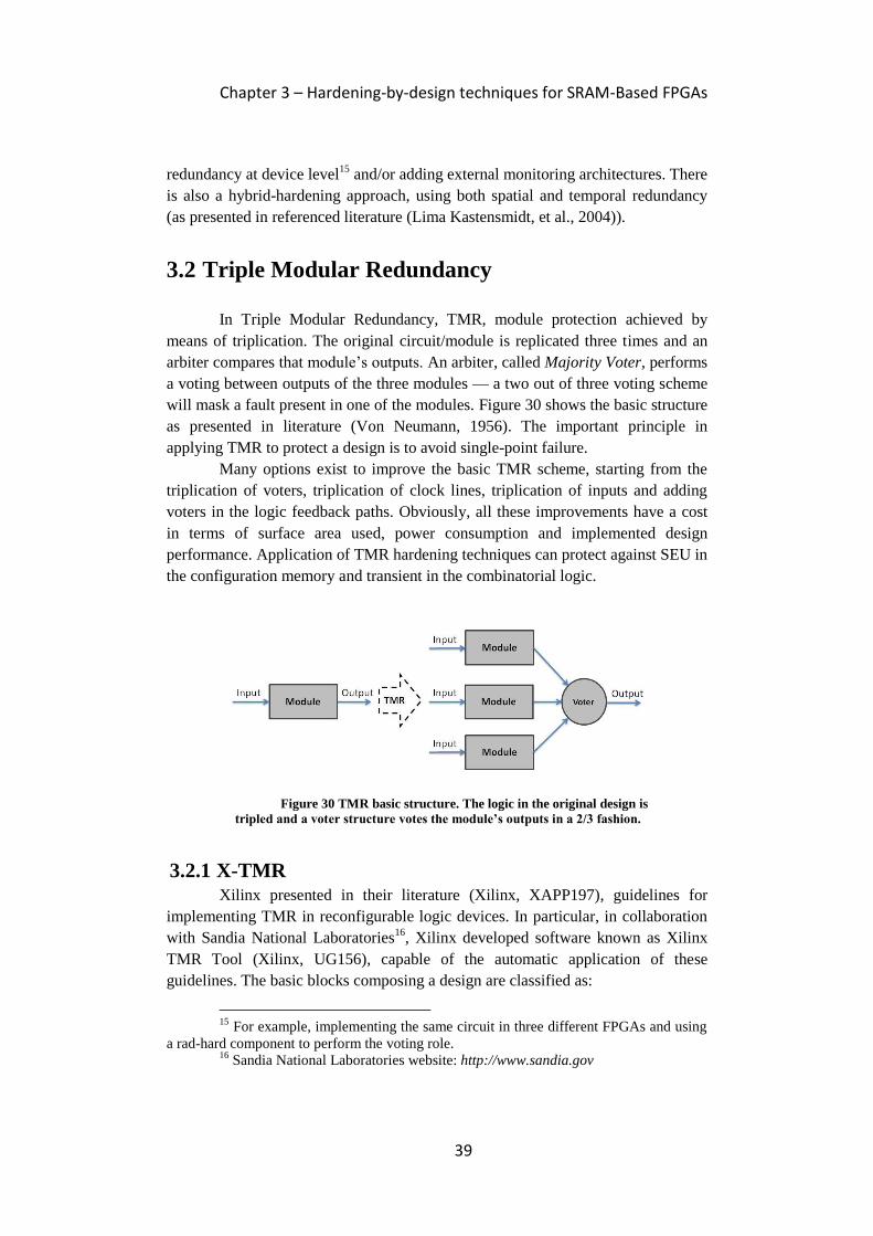
Chapter 3 – Hardening-by-design techniques for SRAM-Based FPGAs
39
redundancy at device level15
and/or adding external monitoring architectures. There
is also a hybrid-hardening approach, using both spatial and temporal redundancy
(as presented in referenced literature (Lima Kastensmidt, et al., 2004)).
3.2 Triple Modular Redundancy
In Triple Modular Redundancy, TMR, module protection achieved by
means of triplication. The original circuit/module is replicated three times and an
arbiter compares that module’s outputs. An arbiter, called Majority Voter, performs
a voting between outputs of the three modules — a two out of three voting scheme
will mask a fault present in one of the modules. Figure 30 shows the basic structure
as presented in literature (Von Neumann, 1956). The important principle in
applying TMR to protect a design is to avoid single-point failure.
Many options exist to improve the basic TMR scheme, starting from the
triplication of voters, triplication of clock lines, triplication of inputs and adding
voters in the logic feedback paths. Obviously, all these improvements have a cost
in terms of surface area used, power consumption and implemented design
performance. Application of TMR hardening techniques can protect against SEU in
the configuration memory and transient in the combinatorial logic.
3.2.1 X-TMR Xilinx presented in their literature (Xilinx, XAPP197), guidelines for
implementing TMR in reconfigurable logic devices. In particular, in collaboration
with Sandia National Laboratories16
, Xilinx developed software known as Xilinx
TMR Tool (Xilinx, UG156), capable of the automatic application of these
guidelines. The basic blocks composing a design are classified as:
15 For example, implementing the same circuit in three different FPGAs and using
a rad-hard component to perform the voting role. 16
Sandia National Laboratories website: http://www.sandia.gov
Figure 30 TMR basic structure. The logic in the original design is
tripled and a voter structure votes the module’s outputs in a 2/3 fashion.

Chapter 3 – Hardening-by-design techniques for SRAM-Based FPGAs
40
Inputs: circuit logic for inputs;
Throughput logic: logic modules in which all the logic paths traverse the
module without forming logical loops, i.e. without feedback paths;
Feedback logic: logic in which feedback paths are present; and
Outputs: logic for circuit outputs.
To protect voter circuitry from SET and SEU, a triplication is needed. To
prevent common failures mode affecting input logics, all inputs must be tripled
outside the device, in the PCB board layout. To further improve mitigation
effectiveness, the clock and reset must be separated for each TMR domain.
This replication prevents a problem arising from SETs in the global signal
lines — in this way, the domains are separated and can operate independently.
Another single point of failure could be the re-convergence of outputs to the
external world — Xilinx’s approach resolves the problem inserting Minority
Voters, as shown in Figure 31. This structure controls the re-convergence of the
signals in the PCB trace. If a SEU affects the output circuit of a domain, the related
Minority Voter will detect this condition and it will place the related output pin in a
high impedance state. These output voters yield no single-point failures, because in
the worst case, if affected by SEU, they will disable a domain output, while the
others will still drive the correct signals. Another characteristic to improve design
reliability is the insertion of Majority Voters in feedback paths. These voters ensure
constant synchronization between redundant state machines. Figure 32 represents
the schematization of the complete application of the X-TMR approach.
Figure 31 Minority Voter structure used to control a circuit’s outputs at PCB level
(source Xilinx User Guide). If an error affects an output domain, a Minority Voter will place
that domain’s output into a high impedance state. Hence, output will be driven by the other two
domains

Chapter 3 – Hardening-by-design techniques for SRAM-Based FPGAs
41
Figure 32 X-TMR application schematic (from Xilinx X-TMR documentation): all the
circuit’s inputs are replicated, as well as the global signals; Majority Voters are inserted in the
feedback paths and their outputs are protected by the Minority Voters.
3.2.2 Partial TMR The application of a full TMR approach can be very expensive in terms of
surface area and device resources. Typically, the resources used for a full TMR are
more than three times the used ones in the original design. This add-on is due to
voter implementation and an increase of routing resources demanded. In some
cases, a simple triplication of all input and outputs would be unfeasible for the
device-limited pin numbers. An alternative approach is the Partial (or Selective)
TMR. This strategy selectively protects parts of a design that are considered more
sensitive to induced faults. An example of the application of this strategy is
implemented by the software BYU-LANL Triple Modular Redundancy, BLTmr17
.
This set of tools, developed through collaboration between Brigham Young
University and Los Alamos National Laboratory (Pratt, et al., 2006), performs the
mitigation of a design using the partial TMR approach. They identify two kinds of
configuration upsets:
Non-persistent configuration upsets: configuration bits that if corrupted
can lead to a fault. When a configuration scrubbing process restores
the correct value, the circuit recovers its correct behavior; and
Persistent configuration upsets: upsets involving configuration
sensitive bits having a persistent repercussion on a circuit’s behavior.
After a configuration scrubbing, also if the involved bit recovers its
correct value, a circuit fails to recover the normal operation condition.
Hence, the upsets in these configuration bits persist after configuration
memory correction, also.
Upsets in persistent configuration bits corrupt the circuit state — a circuit
re-initialization – global reset – is needed to recover from this erroneous condition.
17
BYU’s tools website: http://sourceforge.net/projects/byuediftools/
Chapter 3 – Hardening-by-design techniques for SRAM-Based FPGAs
42
The adopted strategy targets a design’s feedback structure, because these blocks
contribute to persistent errors — upsets can propagate through the feedback logic
corrupting the circuit state. The tool analyzes the circuit design, identifying
feedback structures and input/output blocks of the identified sensitive structures. A
user can selectively mitigate the design blocks. A partial TMR approach can
effectively improve design reliability at a lower cost than a full TMR application.
Obviously, the mitigation approach creates tradeoffs between reliability criteria
requested for the application, performance constraints and available resources.
3.2.3 Problems for TMR implementation Some characteristics of development environment and device architecture
can present some problems for TMR implementation effectiveness.
3.2.3.1 Implementation issues
Implementing a hardening-by-design strategy manually could be quite
complex and difficult. The vendor’s tool tries to simplify the added redundant
structures, and hence, a designer must specify special directive optimizations to be
performed in the synthesis. Optimization could also drop off redundant structures
during the mapping and place and route phases. For this reason, verification of the
mitigated design is a tedious process. A designer has to check for low-level
implementation of a circuit to verify correct employment of the desired redundant
structures.
3.2.3.2 Half Latches
In the Xilinx FPGA architecture, there are components providing logic
constant values (Xilinx, XAPP197). Errors affecting these resources remain
undetected in the bitstream — the circuit behavior can present a faulty behavior
while the configuration memory yields no bit-flips. The constant logic values are
provided using ‘keeper circuits’ present at the input pins of all Configurable Logic
Blocks, CLBs, and I/O blocks. When a logic element needs a logic constant, an
unused routing resource can obtain this constant from the half latch. The polarity of
the signal (i.e. VCC or GND) can be changed inside a CLB or I/O block by means
of a programmable inverter. The half latch is placed in series with the routing wire
and the input pins of the logic block. The half latch is transparent when the routing
connection is carrying an active signal, while it keeps its most recent value when
the routing connection is unused. The last known value is determined at the device
power-up or after a re-initialization by means of the assertion of the FPGA PROG
signal. A particle strike can temporally alter the connection of the half latch,
connecting an active routing channel to the input of this keeper component. This
kind of fault condition remains undetected by the readback process, in particular in
the Virtex family; and persists until a full device re-initialization — whereas, in
Chapter 3 – Hardening-by-design techniques for SRAM-Based FPGAs
43
Xilinx’s newer FPGAs family, the half latch can recover by leaking off (Quinn, et
al., 2008).
The half latch sensitivity can be eliminated by removing the functional
dependencies on the logic constants – VCCs and GNDs – from the user’s design, i.e.
providing external sources for the values. These external sources, in a TMR
approach, have to be tripled for different domains. In literature (Graham, et al.,
2003), the half latch problem is analyzed in detail and extraction techniques, to
remove this source of errors, are presented. In addition, the Xilinx X-TMR tool
provides an automated process to extract the half latches.
3.2.3.3 Multiple Bit Upsets and Domain Cross-Errors
One of the most problematic events that can defeat hardening techniques,
such as TMR, is the Multiple Bit Upset, MBU, phenomenon (Quinn, et al., 2005).
Theoretically, a full TMR hardening design is protected against all single
occurrences of a single error — excluding SEFI problems. An MBU can lead to the
simultaneous corruption of two18
redundant domains. This event is called Domain
Crossing Errors (Quinn, et al., 2007). In presence of two corrupted domains, the
voter structures operate incorrectly and are unable to mask the fault.
3.2.3.4 Single Bit Upsets leading Multiple Effects
Another problem, intrinsic in the Xilinx architecture, is related to single bit
controlling multiple resources. Indeed, as presented in one source (Sterpone, et al.,
2005), there are bits in the configuration memory controlling two or more routing
segments (a description of such possible faults is presented in Chapter 2). Thus, an
SEU affecting one of these bits can modify two or more routing connections,
leading to multiple effects, and possibly corrupting simultaneously two individual
TMR domains. The same authors have proposed (Sonza Reorda, et al., 2005) a
Reliability-Oriented Place and Route Algorithm, RoRA; this placement strategy
guarantees that a single error is incapable of simultaneously corrupting two
separate TMR domains.
3.2.3.5 Domain synchronization and active partial reconfiguration
To refresh the correct configuration memory content, there are two
scrubbing options:
Complete memory re-configuration: all the memory configuration
is re-written and the device functionalities are stopped during the
configuration process; or
Active partial reconfiguration: only a part of the configuration
memory is re-written while implemented circuit functionalities
continue during this process.
18
Or even all the three TMR domains.
Chapter 3 – Hardening-by-design techniques for SRAM-Based FPGAs
44
As FPGAs are evolving, their configuration memory is increasing in
capacity. Hence, a complete reconfiguration process can present a noticeable
downtime for the service a circuit offers. In Xilinx devices, a more sophisticated
approach is exploiting the active partial reconfiguration (Xilinx, XAPP216). If the
domains are properly partitioned, an error detected in a domain could trigger the
reconfiguration of only that domain, keeping the circuit operations running. This
problem arises in re-synchronizing the reconfigured domain with others. Indeed,
the reconfiguration process can refresh the correct circuit’s structure, but it fails to
restore the circuit status (flip-flop contents, state machine status, etc.). In literature
(Azambuja, et al., 2009), a structure to re-synchronize the reconfigured domain is
presented. In addition, feedback voters inserted by the X-TMR tool aim to keep the
three redundant domains synchronized.
3.3 Experimental study of TMR in presence of error
accumulation
We studied the impact of error accumulation on the memory configuration
for hardened designs. In particular, we tested various TMR schemes, analyzing
accumulation error impact on circuit behaviors. We studied the correctness in the
operation of hardened circuits as a function of errors in the configuration memory.
TMR aims to preserve the correct circuit behavior for only one error in the
configuration memory, but this kind of study is useful for the calibration of the
memory-scrubbing rate.
3.3.1 Experimental Setup and Devices For our experiments, we used as our test vehicle, a Spartan-3 XC3S200
FPGA, designed by Xilinx, in a 90 nm CMOS technology. The combination of
low-cost and resource availability makes it suitable for many mainstream
applications, such as the automotive industry, where it is used to implement a
variety of functions spanning from concentrating glue-logic on a single device to
more complex data processing algorithms (e.g. digital audio filtering). In cases
where such devices are used in Electronic Control Units, ECU, managing critical
vehicle functions – steering, braking – it is mandatory to mitigate any effect that
might prevent an FPGA from performing correctly. Conversely, in cases where
such devices are used in non-safety-critical functions, for example in entertainment
control units, ECU; any effect that might prevent that FPGA from working
correctly can reduce, even drastically, the service quality that ECU provides, and
therefore it may have a dramatic impact on end-user perception of product quality.
As a result, in both application scenarios, faults affecting the FPGA must be
properly mitigated.
Chapter 3 – Hardening-by-design techniques for SRAM-Based FPGAs
45
Our test-setup comprises a Device Under Test, DUT, board and a control
board. The control board is equipped with a Xilinx Virtex-2 Pro XC2VP30, whose
embedded PowerPC is used to manage all operations needed for performing both
static and dynamic tests. It can configure and readback the DUT via JTAG,
stimulate the DUT, and monitor resulting output. Radiation testing was performed
in air using an americium source emitting alpha particles with energy of about 5.4
MeV and flux of 1.543 104 alphas s
-1 within a solid angle of 2π sr. The half-life of
241Am is relatively long, 433 years, so the source can be modeled as a constant flux
emitter. The distance between our FPGA and its respective alpha source was
constant throughout our experiments and the component die was completely
exposed using a nitric acid delidding process.
3.3.2 Tested Configurations and Circuits Initially, we performed static tests to estimate the alpha-induced error rate
of the DUT configuration memory controlling the various resources inside the
FPGA. The DUT was loaded with ad-hoc configurations and the americium source
was placed above the exposed die. The control board periodically scanned the DUT
configuration memory searching for bit-flips. Periodically, we also performed a
reconfiguration to prevent excessively large error accumulation. Afterwards,
dynamic tests were carried out, comparing the DUT outputs with those coming
from a golden unit not exposed to radiation. In this context, we use the term SEFI
to identify an error condition at the hardened design outputs. Readback and
reconfiguration were performed either following a SEFI or after a given time
elapsed from the previous readback. The corrupted bitstreams were post-processed
using CILANTO (Bellato, et al., 2006), to trace the bit-flips in the configuration
memory back to the controlled resources inside the FPGA.
One of the applications chosen for the dynamic tests was PicoBlaze, a soft
microcontroller (i.e. a microprocessor implemented using the FPGA fabric) freely
available from Xilinx (Xilinx, UG129). A PicoBlaze consists of 16 8-bit registers,
a 64-byte scratchpad RAM, a 1k-byte instruction ROM, and an 8-bit ALU. It
occupies about 5 percent of XC3S200 resources, performing 44 MIPS with a clock
of 50 MHz. PicoBlaze was loaded with an assembly code implementing the
functionality of an average moving filter. To maximize resource usage and create
an easy-to-partition design to apply hardening techniques, we linked four
individual PicoBlaze units as shown in Figure 33a. All the PicoBlaze instances
perform the same task (a simple averaging filter). Outputs of a chain element are
connected to the inputs of the subsequent stage. After assessing the sensitivity of
the unhardened circuit to alpha particles, we applied different mitigation schemes
based on TMR. In particular, we adopted the following three solutions:
One-voter TMR: the design is replicated three times and a majority
voter is placed at the circuit output performing a bit-by-bit voting
(Figure 33b);
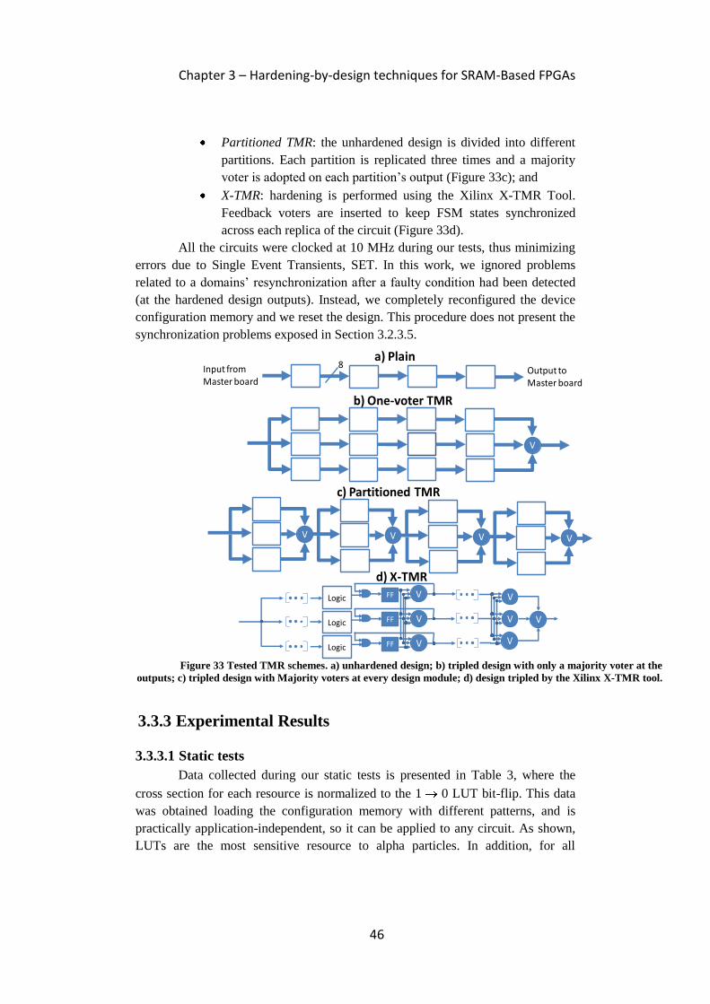
Chapter 3 – Hardening-by-design techniques for SRAM-Based FPGAs
46
Partitioned TMR: the unhardened design is divided into different
partitions. Each partition is replicated three times and a majority
voter is adopted on each partition’s output (Figure 33c); and
X-TMR: hardening is performed using the Xilinx X-TMR Tool.
Feedback voters are inserted to keep FSM states synchronized
across each replica of the circuit (Figure 33d).
All the circuits were clocked at 10 MHz during our tests, thus minimizing
errors due to Single Event Transients, SET. In this work, we ignored problems
related to a domains’ resynchronization after a faulty condition had been detected
(at the hardened design outputs). Instead, we completely reconfigured the device
configuration memory and we reset the design. This procedure does not present the
synchronization problems exposed in Section 3.2.3.5.
Figure 33 Tested TMR schemes. a) unhardened design; b) tripled design with only a majority voter at the
outputs; c) tripled design with Majority voters at every design module; d) design tripled by the Xilinx X-TMR tool.
3.3.3 Experimental Results
3.3.3.1 Static tests
Data collected during our static tests is presented in Table 3, where the
cross section for each resource is normalized to the 1 0 LUT bit-flip. This data
was obtained loading the configuration memory with different patterns, and is
practically application-independent, so it can be applied to any circuit. As shown,
LUTs are the most sensitive resource to alpha particles. In addition, for all
8Input fromMaster board
Output toMaster board
V
V V V V
Logic VFF
Logic VFF
Logic VFF
V
V
V
a) Plain
b) One-voter TMR
c) Partitioned TMR
d) X-TMR
V
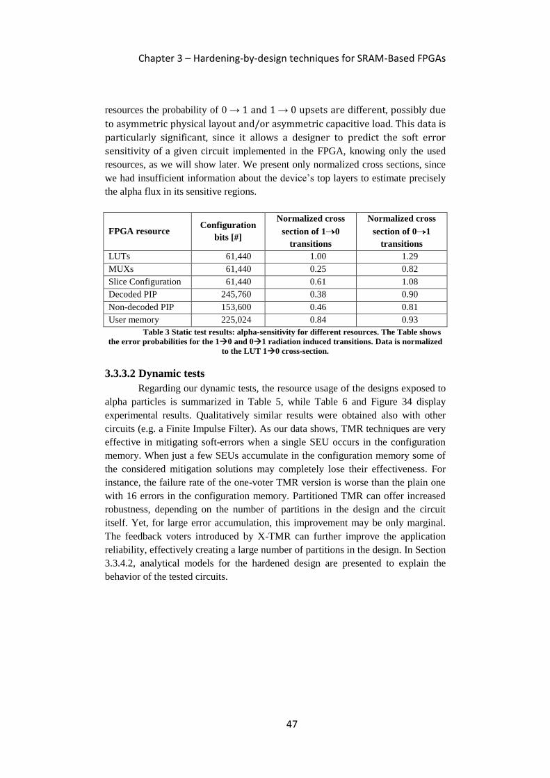
Chapter 3 – Hardening-by-design techniques for SRAM-Based FPGAs
47
resources the probability of 0 → 1 and 1 → 0 upsets are different, possibly due
to asymmetric physical layout and/or asymmetric capacitive load. This data is
particularly significant, since it allows a designer to predict the soft error
sensitivity of a given circuit implemented in the FPGA, knowing only the used
resources, as we will show later. We present only normalized cross sections, since
we had insufficient information about the device’s top layers to estimate precisely
the alpha flux in its sensitive regions.
FPGA resource Configuration
bits [#]
Normalized cross
section of 1 0
transitions
Normalized cross
section of 0 1
transitions
LUTs 61,440 1.00 1.29
MUXs 61,440 0.25 0.82
Slice Configuration 61,440 0.61 1.08
Decoded PIP 245,760 0.38 0.90
Non-decoded PIP 153,600 0.46 0.81
User memory 225,024 0.84 0.93
Table 3 Static test results: alpha-sensitivity for different resources. The Table shows
the error probabilities for the 10 and 01 radiation induced transitions. Data is normalized
to the LUT 10 cross-section.
3.3.3.2 Dynamic tests
Regarding our dynamic tests, the resource usage of the designs exposed to
alpha particles is summarized in Table 5, while Table 6 and Figure 34 display
experimental results. Qualitatively similar results were obtained also with other
circuits (e.g. a Finite Impulse Filter). As our data shows, TMR techniques are very
effective in mitigating soft-errors when a single SEU occurs in the configuration
memory. When just a few SEUs accumulate in the configuration memory some of
the considered mitigation solutions may completely lose their effectiveness. For
instance, the failure rate of the one-voter TMR version is worse than the plain one
with 16 errors in the configuration memory. Partitioned TMR can offer increased
robustness, depending on the number of partitions in the design and the circuit
itself. Yet, for large error accumulation, this improvement may be only marginal.
The feedback voters introduced by X-TMR can further improve the application
reliability, effectively creating a large number of partitions in the design. In Section
3.3.4.2, analytical models for the hardened design are presented to explain the
behavior of the tested circuits.
Chapter 3 – Hardening-by-design techniques for SRAM-Based FPGAs
48
Design LUT
bits
MUX
bits
CFG
bits
DPIP
bits
NPIP
bits
#
Voters
Resource
overhead
[%]
Unhardened
PicoBlaze chain 9,488 3,276 1,699 8,570 4,759 0 100
One-voter TMR
PicoBlaze chain 29,232 9,878 5,317 27,301 15,428 8 314
Partitioned
TMR PicoBlaze
chain
29,968 10,051 5,584 28,330 16,089 32 324
X-TMR
PicoBlaze chain 34,800 10,643 6,956 36,283 23,292 344 403
Table 4 Resource occupied by the tested designs. The table shows the used CLB
resources and presents the overhead for the hardened solutions with respect to the plain circuit.
Design
SEFI/min,
reconfiguring
after 5 bit-flips
in the CFM
SEFI/min,
reconfiguring
after 10 bit-
flips in the
CFM
SEFI/min,
reconfiguring
after 16 bit-
flips in the
CFM
SEFI/min
reconfiguring
only after a
SEFI
Unhardened PicoBlaze 0.35 0.87 0.88 1.16
One-voter TMR PicoBlaze 0.18 0.65 0.90 1.43
Partitioned TMR PicoBlaze 0.06 0.22 0.36 0.91
X-TMR PicoBlaze 0.03 0.14 0.17 0.51
Table 5 Alpha source experimental results for dynamic circuits. In this case, the term
SEFI refers to errors at the hardened design outputs. Columns present probability of an error
at the circuit outputs as a function of the accumulated errors in the configuration memory. The
last column shows the average number of accumulated errors to defeat the circuit functionality.
3.3.4 Analytical Model
3.3.4.1 Unhardened designs
Previous work (Sterpone, et al., 2005) showed that, assuming only a single
bit-flip in the configuration memory, a worst-case estimation of the sensitivity of a
circuit is given by the number of used bits divided by the total number of
configuration memory bits. From the collected static data and from the analysis of
the used resources, we developed a refined model to predict the failure probability
in presence of multiple SEUs in the configuration memory. This model can be
summarized by Equation 1, where n1,resource (n0,resource) is the number of
configuration memory bits set to 1 (0) relative to a given resource in the slices used
by the circuit, see Table 4; w1,resource (w0,resource) is the probability that a 1 0
(0 1) transition in the configuration memory bits controlling resource leads to a
functional interruption; resource,1 0 ( resource,0 1) is the experimental upset cross
section of the configuration memory bits for 1 0 (0 1) transitions controlling
resource, see Table 3; d1,resource is the density of 1’s and must be included for the

Chapter 3 – Hardening-by-design techniques for SRAM-Based FPGAs
49
routing resources, where the probability an added resource will interfere with
circuit functionality increases with the number of resources of that type already
present. A precise estimation of d1,resource would require the evaluation of each single
switching matrix, whereas a rough estimation can be obtained by averaging over
the whole design.
Concerning wx,esource, bit flips in a LUT used to implement a logic function
inside an FPGA will result in an error at the outputs regardless of being 0 1 or
1 0 transitions — obviously assuming the workload uses that LUT, hence w1,LUT
and w0,LUT are equal to 1. Conversely, bit flips in the configuration memory
controlling non-decoded PIPs will surely impact the application in the case of 1 0
transitions, since those correspond to the removal of existing connections; but they
may or may not have an impact in the case of 0 1 transitions, since those
correspond to the addition of a path which may or may not interfere with existing
connections. Of course, the larger the number of interconnections, the higher the
probability an added interconnection interferes with the application routing. This
turns into the necessity of including d1,non-decoded PIPs in the calculation. Equation 1
states that the dynamic sensitivity of an FPGA is less than its static sensitivity, in
other words, not all the bit-flips in the configuration memory lead to an error at the
outputs, depending on various parameters.
resourcesall
resourceresourceresourceresourceresourceresourceresourcedesign dwnwn ][ ,110,,0,001,,1,1
Equation 1 Analytical model to estimate the sensitivity of unhardened circuits.
Equation 1 can be used to compare the sensitivities of different circuits
implemented in the FPGA. For each different pair of designs we want to compare,
we measure the dynamic cross section in terms of SEFI/min reconfiguring only
after SEFI (see Table 5) and calculate their ratio. This tells us experimentally
which is the more sensitive design and by what amount. Afterwards, we compare
this number with the predicted ratio between the design’s cross sections as
calculated with Equation 1. The coefficients in Equation 1 are obtained as follows:
normalized cross sections for the single resources in Equation 1
are experimental (e.g. Table 3)
number and density of used resources are evaluated analyzing the
bitstreams (e.g. Table 4)
weights are chosen based on simple considerations on the FPGA
structure
We compared a broad range of combinational and sequential designs,
including the PicoBlaze application as noted in this document, both experimentally
and with our analytical model, and found an agreement ranging from 5 to 10
percent between measurements and analytical predictions.
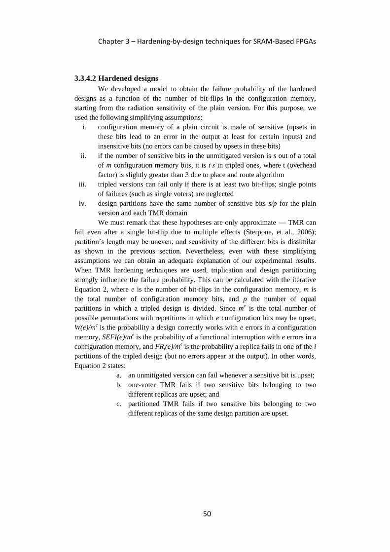
Chapter 3 – Hardening-by-design techniques for SRAM-Based FPGAs
50
3.3.4.2 Hardened designs
We developed a model to obtain the failure probability of the hardened
designs as a function of the number of bit-flips in the configuration memory,
starting from the radiation sensitivity of the plain version. For this purpose, we
used the following simplifying assumptions:
i. configuration memory of a plain circuit is made of sensitive (upsets in
these bits lead to an error in the output at least for certain inputs) and
insensitive bits (no errors can be caused by upsets in these bits)
ii. if the number of sensitive bits in the unmitigated version is s out of a total
of m configuration memory bits, it is t∙s in tripled ones, where t (overhead
factor) is slightly greater than 3 due to place and route algorithm
iii. tripled versions can fail only if there is at least two bit-flips; single points
of failures (such as single voters) are neglected
iv. design partitions have the same number of sensitive bits s/p for the plain
version and each TMR domain
We must remark that these hypotheses are only approximate — TMR can
fail even after a single bit-flip due to multiple effects (Sterpone, et al., 2006);
partition’s length may be uneven; and sensitivity of the different bits is dissimilar
as shown in the previous section. Nevertheless, even with these simplifying
assumptions we can obtain an adequate explanation of our experimental results.
When TMR hardening techniques are used, triplication and design partitioning
strongly influence the failure probability. This can be calculated with the iterative
Equation 2, where e is the number of bit-flips in the configuration memory, m is
the total number of configuration memory bits, and p the number of equal
partitions in which a tripled design is divided. Since me is the total number of
possible permutations with repetitions in which e configuration bits may be upset,
W(e)/me is the probability a design correctly works with e errors in a configuration
memory, SEFI(e)/me is the probability of a functional interruption with e errors in a
configuration memory, and FRi(e)/me is the probability a replica fails in one of the i
partitions of the tripled design (but no errors appear at the output). In other words,
Equation 2 states:
a. an unmitigated version can fail whenever a sensitive bit is upset;
b. one-voter TMR fails if two sensitive bits belonging to two
different replicas are upset; and
c. partitioned TMR fails if two sensitive bits belonging to two
different replicas of the same design partition are upset.
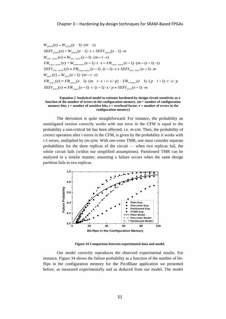
Chapter 3 – Hardening-by-design techniques for SRAM-Based FPGAs
51
meSEFIpstieFReSEFI
pipstipeFRpsistmeFReFR
stmeWeW
meSEFIsteFReSEFI
stmeFRsteWeFR
stmeWeW
meSEFIseWeSEFI
smeWeW
partpartipart
partipartiparti
partpart
voteronevoteronevoterone
voteronevoteronevoterone
voteronevoterone
plainplainplain
plainplain
)1(/)1()1()(
,...2,1/)1()1()/()1()(
)()1()(
)1()1()1()(
))1(()1()1()(
)()1()(
)1()1()(
)()1()(
1
1
11
Equation 2 Analytical model to estimate hardened-by-design circuit sensitivity as a
function of the number of errors in the configuration memory. (m = number of configuration
memory bits, s = number of sensitive bits, t = overhead factor, e = number of errors in the
configuration memory)
The derivation is quite straightforward. For instance, the probability an
unmitigated version correctly works with one error in the CFM is equal to the
probability a non-critical bit has been affected, i.e. m-s/m. Then, the probability of
correct operation after i errors in the CFM, is given by the probability it works with
i-1 errors, multiplied by (m-s)/m. With one-voter TMR, one must consider separate
probabilities for the three replicas of the circuit — when two replicas fail, the
whole circuit fails (within our simplified assumptions). Partitioned TMR can be
analyzed in a similar manner, assuming a failure occurs when the same design
partition fails in two replicas.
Figure 34 Comparison between experimental data and model.
Our model correctly reproduces the observed experimental results. For
instance, Figure 34 shows the failure probability as a function of the number of bit-
flips in the configuration memory for the PicoBlaze application we presented
before, as measured experimentally and as deduced from our model. The model
0 20 40 60 80 1000.0
0.2
0.4
0.6
0.8
1.0
Fa
ilu
re P
rob
ab
ilit
y
Bit-flips in the Configuration Memory
Plain Exp.
One-voter Exp.
Partitioned Exp.
XTMR Exp.
Plain Model
One-voter Model
Partitioned Model
Chapter 3 – Hardening-by-design techniques for SRAM-Based FPGAs
52
parameters were m=1,000,000 (the number of configuration bits in the whole
FPGA under test), s=27,792 the number of sensitive bits (see Table 4), p=4 (the
number of equal design partitions), t=3.23 (the overhead factor for the tripled
versions). At present, a model for the X-TMR version remains undeveloped.
Interestingly enough, for small (the number depends on the implemented
application) accumulations of bit-flips in the configuration memory, triplication
reduces the failure rate of the circuits examined. Yet, as the number of errors which
are permitted to accumulate in the configuration memory grows, one-voter TMR
loses its effectiveness with respect to the unmitigated version. Partitioned TMR
helps to reduce the failure probability also with a larger numbers of bit-flips as
compared to one-voter TMR. The maximum number of errors in the configuration
memory for which triplication is effective depends on the overhead factor, the
number of partitions in the design, and the extent of each partition.

Chapter 3 – Hardening-by-design techniques for SRAM-Based FPGAs
53
3.4 Redundant Residue Number System
We considered another hardening-by-design technique, based on the
Residue Number Systems, RNS, exploiting the properties of the modular
arithmetic. RNS theory was invented around the third century AD by Chinese
mathematician Sun Tzu, and rediscovered in the 1950s for implementing fast
arithmetic and fault tolerant computations. We studied the use of RNS to
implement FIR filters with error correction capabilities. Due to the modular nature
of this arithmetic system, a dedicated module processes each residue digit
separately. This property leads to limited fault propagation and a modular circuit
implementation, which uses fewer resources as compared to TMR-based solutions.
An RNS filter is composed of:
1) B2R: a binary to residue converter;
2) RNSFIR: a set of independent modules performing filtering
operation in the RNS domain; and
3) R2B: a reverse converter performing residue to binary conversion.
Previous works based on RNS exploited the modular arithmetic properties to
achieve error detection and correction capabilities. The so-called Redundant RNS,
RRNS, uses additional modules performing the filtering operation and an error
correction block, ECB.
The RRNS approach can correct errors in hardware performing the binary
to residue conversion, B2R, and the filtering operation in the RNS domain,
RNSFIR, but it gives no guarantee that a fault affecting reverse conversion blocks,
R2B, or affecting error correction blocks, ECB, is corrected.
This work has been carried out in collaboration with Università Tor
Vergata — we validated a new voter implementation to mask faults in these
blocks. This voter can correct errors in all the modules composing the RRNS filter
allowing implementation of a totally fault tolerant FIR filter. The presented voter
requires a very low number of FPGA resources and makes it possible to save more
than 33 percent resource usage with respect to a rough TMR implementation of the
block performing RNS based error correction. We performed radiation tests
implementing the hardened circuit on a Xilinx Spartan-3 FPGA exposed to alpha
particles emitted by an americium alpha source. A monitor board stimulates the
implemented FIR, comparing the DUT outputs with expected ones (coming from a
golden unit). The collected data shows the system can correct faults inside all
RRNS FIR filter blocks.
3.4.1 Residue Number System Background A Residue Number System, RNS, is defined by a set of relatively prime
numbers {m1, m2, …, mp} where the generic mi element is called modulo. The
Chapter 3 – Hardening-by-design techniques for SRAM-Based FPGAs
54
dynamic range of the system M is defined by the product of the modules, i.e.
.
In the RNS system M with modules {m1, m2, …, mp}, we can express the
integer number X with as:
1 2, , ,
p
RNS
m m mX X X X
where . In an RNS domain, operations such as multiplication
and addition can be performed as:
1 11
RNS
mod ( ) mod
X op Y
mod ( ) modp p
m m 1
p m m p
Z m X op Y m
Z
Z m X op Y m
This expression states that an addition or multiplication in the RNS domain can be
performed in a parallel fashion, reducing the original computation in several
modular computation of reduced size. Moreover, the computation in every module
is independent of the other modules, so the computation can be performed
independently for each module. More complete details and proof of the residue
computation can be found in referenced material (Szabó, et al., 1967).
Conversion of a value Z in the RNS domain to the integer domain can be
calculated using the Chinese Remainder Theorem, CRT (Cormen, et al., 2003):
1
1
( ,..., )p i
p
m m m i i
i M
Z CRT Z Z Z k M
where and are obtained by equation: .
A generic Finite Impulse Response, FIR, filter with N tap, can be expressed in the
RNS domain by the equation:
1 111
1
1
01
01
0
( ) ( )
( ) ( )
( ) ( )p pp
p
p
N
m k mmm
k mN
RNS
k
kN
m k mmmk
m
Y n a x n k
y n a x n k
Y n a x n k
Hence, the FIR filter computation in the RNS domain can be performed (Figure
35):
1. Reducing modulo mi the input x(n). The operation provides the residue
digits xmi;

Chapter 3 – Hardening-by-design techniques for SRAM-Based FPGAs
55
2. For each modulo, the modular filter computes the residue Ymi and
every modular filter is independent of the others; and
3. The result y(n) in the integer domain is obtained with the CRT
conversion.
Figure 35 Basic block scheme of a FIR filter implemented using the RRNS technique.
If a circuit performs mainly addition and multiplication, it can take advantage of
the improvement given by the computation in the RNS domain. The conversions
present an overhead, but these operations can be performed efficiently in an FPGA
(Re, et al., 2001).
The capability to detect and correct errors in a residue number system is
had by adding additional modules. In a Redundant Residue Number System, RRNS,
there are k modules and additional r modules; the latter are called redundant
modules. The product of all the modules is defined as the total range of the system:
The total range can be split into two adjacent intervals:
Legitimate range [0, M-1], where is the product of
the non redundant moduli, or
Illegitimate range [M, MT-1] where is the product
of all the modules defining the system.
The mi projection of a number X, in the RNS domain, is defined as the
residue vector ), i.e. representation of the value X
without the ith residue digit. In an RRNS system, with two redundant modules
(r=2), if an error affects the element i, then the Xi projection falls into a legitimate
range, while all other Xj projections (with j≠i), fall into the illegitimate range. The
proof of the RRNS properties is discussed in literature (Barsi, et al., 1973). This
property determines the error detection and correction capabilities in an RRNS:
Detection: there are projections falling in the illegitimate range, the
faulty module is the one with the mi-projection belonging to the
legitimate range; and
Correction: the correct values of X can be obtained by performing
the reverse conversion of the Xi projection.
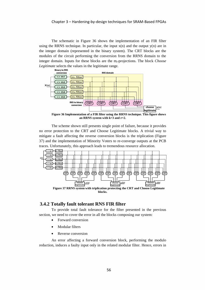
Chapter 3 – Hardening-by-design techniques for SRAM-Based FPGAs
56
The schematic in Figure 36 shows the implementation of an FIR filter
using the RRNS technique. In particular, the input x(n) and the output y(n) are in
the integer domain (represented in the binary system). The CRT blocks are the
modules of the circuit performing the conversion from the RRNS domain to the
integer domain. Inputs for these blocks are the mi-projections. The block Choose
Legitimate selects the values in the legitimate range.
Figure 36 Implementation of a FIR filter using the RRNS technique. This figure shows
an RRNS system with k=3 and r=2.
The scheme shown still presents single point of failure, because it provides
no error protection to the CRT and Choose Legitimate blocks. A trivial way to
mitigate a fault affecting the reverse conversion blocks is the triplication (Figure
37) and the implementation of Minority Voters to re-converge outputs at the PCB
traces. Unfortunately, this approach leads to tremendous resource allocation.
Figure 37 RRNS system with triplication protecting the CRT and Choose Legitimate
blocks.
3.4.2 Totally fault tolerant RNS FIR filter To provide total fault tolerance for the filter presented in the previous
section, we need to cover the error in all the blocks composing our system:
Forward conversion
Modular filters
Reverse conversion
An error affecting a forward conversion block, performing the modulo
reduction, induces a faulty input only in the related modular filter. Hence, errors in
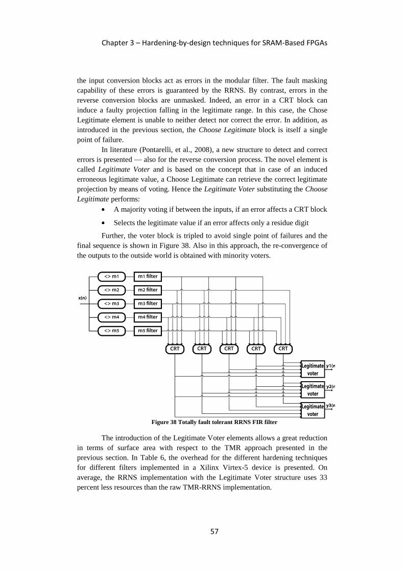
Chapter 3 – Hardening-by-design techniques for SRAM-Based FPGAs
57
the input conversion blocks act as errors in the modular filter. The fault masking
capability of these errors is guaranteed by the RRNS. By contrast, errors in the
reverse conversion blocks are unmasked. Indeed, an error in a CRT block can
induce a faulty projection falling in the legitimate range. In this case, the Chose
Legitimate element is unable to neither detect nor correct the error. In addition, as
introduced in the previous section, the Choose Legitimate block is itself a single
point of failure.
In literature (Pontarelli, et al., 2008), a new structure to detect and correct
errors is presented — also for the reverse conversion process. The novel element is
called Legitimate Voter and is based on the concept that in case of an induced
erroneous legitimate value, a Choose Legitimate can retrieve the correct legitimate
projection by means of voting. Hence the Legitimate Voter substituting the Choose
Legitimate performs:
A majority voting if between the inputs, if an error affects a CRT block
Selects the legitimate value if an error affects only a residue digit
Further, the voter block is tripled to avoid single point of failures and the
final sequence is shown in Figure 38. Also in this approach, the re-convergence of
the outputs to the outside world is obtained with minority voters.
Figure 38 Totally fault tolerant RRNS FIR filter
The introduction of the Legitimate Voter elements allows a great reduction
in terms of surface area with respect to the TMR approach presented in the
previous section. In Table 6, the overhead for the different hardening techniques
for different filters implemented in a Xilinx Virtex-5 device is presented. On
average, the RRNS implementation with the Legitimate Voter structure uses 33
percent less resources than the raw TMR-RRNS implementation.
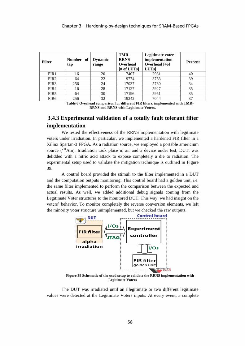
Chapter 3 – Hardening-by-design techniques for SRAM-Based FPGAs
58
Filter Number of
tap
Dynamic
range
TMR-
RRNS
Overhead
[# of LUTs]
Legitimate voter
implementation
Overhead [#of
LUTs]
Percent
FIR1 16 20 7407 2931 40
FIR2 64 22 9774 3763 39
FIR3 256 24 17037 5780 34
FIR4 16 28 17127 5927 35
FIR5 64 30 17196 5951 35
FIR6 256 32 19242 7044 37
Table 6 Overhead comparison for different FIR filters, implemented with TMR-
RRNS and RRNS with Legitimate Voters.
3.4.3 Experimental validation of a totally fault tolerant filter
implementation We tested the effectiveness of the RRNS implementation with legitimate
voters under irradiation. In particular, we implemented a hardened FIR filter in a
Xilinx Spartan-3 FPGA. As a radiation source, we employed a portable americium
source (241
Am). Irradiation took place in air and a device under test, DUT, was
delidded with a nitric acid attack to expose completely a die to radiation. The
experimental setup used to validate the mitigation technique is outlined in Figure
39.
A control board provided the stimuli to the filter implemented in a DUT
and the computation outputs monitoring. This control board had a golden unit, i.e.
the same filter implemented to perform the comparison between the expected and
actual results. As well, we added additional debug signals coming from the
Legitimate Voter structures to the monitored DUT. This way, we had insight on the
voters’ behavior. To monitor completely the reverse conversion elements, we left
the minority voter structure unimplemented, but we checked the raw outputs.
Figure 39 Schematic of the used setup to validate the RRNS implementation with
Legitimate Voters
The DUT was irradiated until an illegitimate or two different legitimate
values were detected at the Legitimate Voters inputs. At every event, a complete
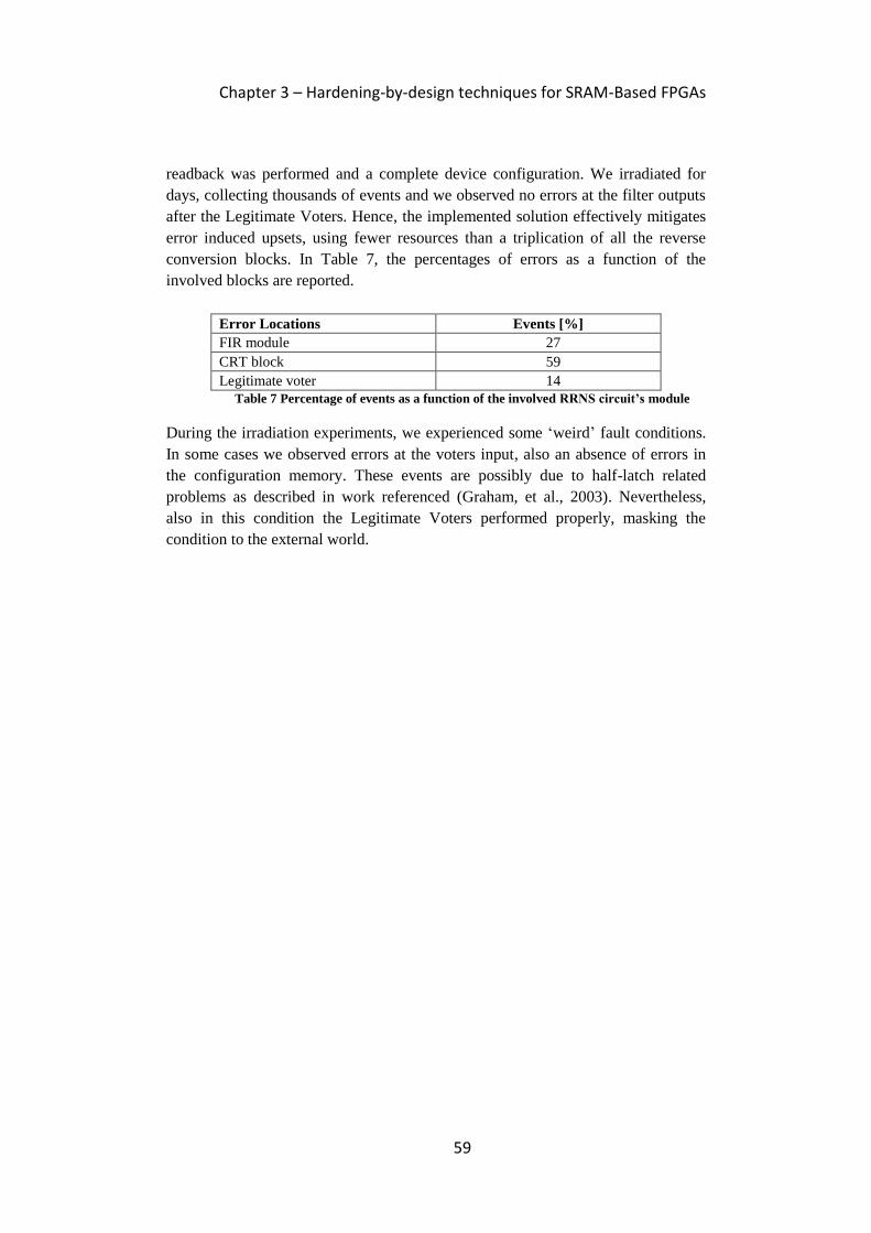
Chapter 3 – Hardening-by-design techniques for SRAM-Based FPGAs
59
readback was performed and a complete device configuration. We irradiated for
days, collecting thousands of events and we observed no errors at the filter outputs
after the Legitimate Voters. Hence, the implemented solution effectively mitigates
error induced upsets, using fewer resources than a triplication of all the reverse
conversion blocks. In Table 7, the percentages of errors as a function of the
involved blocks are reported.
Error Locations Events [%]
FIR module 27
CRT block 59
Legitimate voter 14
Table 7 Percentage of events as a function of the involved RRNS circuit’s module
During the irradiation experiments, we experienced some ‘weird’ fault conditions.
In some cases we observed errors at the voters input, also an absence of errors in
the configuration memory. These events are possibly due to half-latch related
problems as described in work referenced (Graham, et al., 2003). Nevertheless,
also in this condition the Legitimate Voters performed properly, masking the
condition to the external world.


Chapter 3 – Hardening-by-design techniques for SRAM-Based FPGAs
61
3.5 Multiple Bit Upsets in TMR circuits
Multiple Bit Upsets (MBUs) are becoming a growing concern with the
advent of the newest SRAM-based FPGA devices. Nowadays, scarce data is
available on the effectiveness of TMR hardening technique when coping with
MBUs. However, it is expected that as MBUs produce multiple upsets in the
configuration memory, they are more likely than SEUs to induce domain-crossing
events that may affect two or more TMR modules; thus limiting the effectiveness
of TMR. As a result, the characterization of the design robustness against MBUs is
becoming a critical task, which can be much more complex than studying the
robustness against SEUs. Actually, several tools are available for studying SEU
sensitivity, while few tools suitable for studying MBUs are available. In case
accelerated radiation testing is used, setting up experiments to observe MBU
effects is much more complex than for SEUs. It is indeed very difficult to
discriminate between the accumulation of SEUs, and the occurrence of MBUs as
information on the physical location of configuration memory bits is seldom
available, and therefore it is generally impossible to know whether the multiple
upsets observed are real MBUs or accumulated SEUs.
In case fault injection is used, the lack of information about the physical
location of configuration memory bits makes it very difficult to identify which bits
have to be simultaneously flipped to emulate real MBUs. The same holds for
alternative techniques based on static analysis (i.e. without the use of simulation) of
the design. As a result, the knowledge of the physical location of configuration
memory bits is becoming more important for studying MBUs than before with
SEUs. As device manufacturers are normally withholding such information, an
approach to extract it and use it during design analysis is needed.
In this section, we present a methodology suitable for analyzing the
sensitivity of circuits implemented in SRAM-based FPGAs, and adopting the TMR
mitigation scheme. The methodology has two steps — a device characterization
step performed using laser testing, and a design analysis step performed using a
layout-aware static analyzer tool.
Laser testing aims to investigate the physical structure of the FPGA used to
implement the design. Through localized photoelectric stimulation, configuration
memory organization is deduced, thus identifying where configuration memory bits
are laid out on the silicon surface. By knowing their spatial location, it is possible
to identify which bits are close and hence likely to be affected by MBUs. This will
allow one to discriminate between accumulated SEUs and MBUs during
accelerated radiation testing, and serve as starting point for the following module.
The static analyzer tool performs the analysis of the design the FPGA
implements, and it generates a classification of the possible MBUs affecting the
Chapter 3 – Hardening-by-design techniques for SRAM-Based FPGAs
62
TMR architecture. Static analyzer information includes the orientation of the
MBUs within the configuration memory and the resulting effects. The tool has
been extended from the version developed in by others (Sterpone, et al., 2008). A
new database storing data about the layout of the configuration memory has been
added, based on information provided by laser testing. The current implementation
of the tool considers 2-bit MBUs, and bits are clustered together for MBU analysis
considering their physical adjacency, exploiting the intuitive concept that closely
placed bits are more likely to be the site of MBUs than bits more distantly placed.
We developed the methodology targeting Xilinx SRAM-based FPGAs. In
this work, we used as a test vehicle a Xilinx Virtex-II Pro device. In particular, the
device used for the laser tests is a Xilinx XC2VP30; it features a bitstream size of
11,589,920 bits. However, the methodology is general, and it can be applied to
other devices from other manufacturers, if such device can be attacked using laser
testing (photoelectric stimulation from the substrate must be possible), and
readback of configuration memory is supported by the device.
3.5.1 Analysis Methodology The purpose of our methodology is to analyze the effects of MBUs in the
configuration memory of SRAM-based FPGAs as soon as a model of the placed
and routed design is available. To reach such a goal, a preliminary step is needed to
characterize the device used to implement the design, to obtain some details about
its physical structure — details usually withheld manufacturers. This
characterization phase is time consuming, and resource demanding; however, as
with accelerated radiation ground testing experiments, it is required only when new
devices are adopted. Once obtained, the results of the characterization step can be
used for any design exploiting the same device. The characterization is performed
by means of laser testing as described in Section 3.5.2. Once the characterization is
completed, the gathered physical information is exploited by a modified version of
the static analyzer tool as developed by Politecnico di Torino.
3.5.2 Device characterization using laser testing Previous works (Miller, 2006), (Miller, et al., 2006) and (Bocquillon, et al.,
2007) have shown that lasers can be used as an efficient complementary tool to
accelerator testing in order to evaluate the sensitivity of electronic components
exposed to radiation and also trigger various single event effects, SEEs. Regarding
the complexity of SRAM-based architecture, a laser is especially useful since it can
inject charges with spatial localization and temporal precision. In this work, the
capabilities of lasers are exploited for a different purpose. Faults are injected
through photoelectric stimulation at regularly spaced spots, thus creating a matrix
of points on the FPGA surface. After each laser injection, the whole configuration
memory is read, and analyzed to identify the correlation between spatial positions
of configuration memory bits.
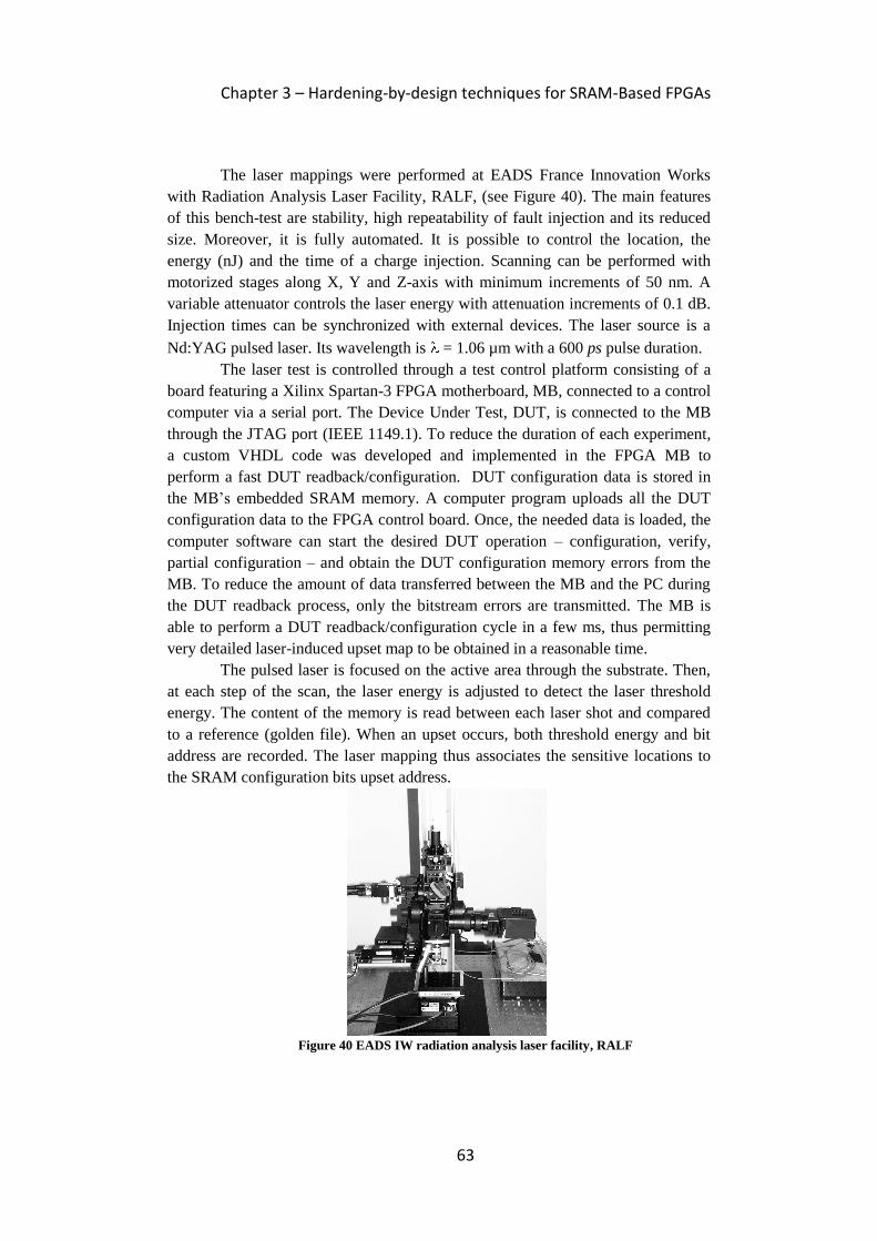
Chapter 3 – Hardening-by-design techniques for SRAM-Based FPGAs
63
The laser mappings were performed at EADS France Innovation Works
with Radiation Analysis Laser Facility, RALF, (see Figure 40). The main features
of this bench-test are stability, high repeatability of fault injection and its reduced
size. Moreover, it is fully automated. It is possible to control the location, the
energy (nJ) and the time of a charge injection. Scanning can be performed with
motorized stages along X, Y and Z-axis with minimum increments of 50 nm. A
variable attenuator controls the laser energy with attenuation increments of 0.1 dB.
Injection times can be synchronized with external devices. The laser source is a
Nd:YAG pulsed laser. Its wavelength is = 1.06 µm with a 600 ps pulse duration.
The laser test is controlled through a test control platform consisting of a
board featuring a Xilinx Spartan-3 FPGA motherboard, MB, connected to a control
computer via a serial port. The Device Under Test, DUT, is connected to the MB
through the JTAG port (IEEE 1149.1). To reduce the duration of each experiment,
a custom VHDL code was developed and implemented in the FPGA MB to
perform a fast DUT readback/configuration. DUT configuration data is stored in
the MB’s embedded SRAM memory. A computer program uploads all the DUT
configuration data to the FPGA control board. Once, the needed data is loaded, the
computer software can start the desired DUT operation – configuration, verify,
partial configuration – and obtain the DUT configuration memory errors from the
MB. To reduce the amount of data transferred between the MB and the PC during
the DUT readback process, only the bitstream errors are transmitted. The MB is
able to perform a DUT readback/configuration cycle in a few ms, thus permitting
very detailed laser-induced upset map to be obtained in a reasonable time.
The pulsed laser is focused on the active area through the substrate. Then,
at each step of the scan, the laser energy is adjusted to detect the laser threshold
energy. The content of the memory is read between each laser shot and compared
to a reference (golden file). When an upset occurs, both threshold energy and bit
address are recorded. The laser mapping thus associates the sensitive locations to
the SRAM configuration bits upset address.
Figure 40 EADS IW radiation analysis laser facility, RALF

Chapter 3 – Hardening-by-design techniques for SRAM-Based FPGAs
64
We applied our characterization method to a Xilinx Virtex II device.
Although dated, this component is representative of complex devices that can be
studied using such characterization methodology. Noting, it is still interesting for
space application thanks to availability of parts housed in hermetic packages. By
laser mapping the FPGA surface – producing the spatial location of configuration
memory bits – and their bitstream addresses (FAR address in Xilinx terminology),
it is possible to identify which resource is placed next to the other. Data is collected
to a database in a suitable format and then exploited by our static analyzer tool as
described in the following section.
Figure 41 Results of a Virtex II device characterization, for 200x100µm2 a die section
During device characterization, we scanned a silicon surface implementing
one Configurable Logic Block, CLB, and its neighboring area. Since the FPGA
array is regular, it is possible to reuse such analysis for any other CLB on the
similar device family.
Figure 41 represents a section of 200x100 m2 of the silicon area
corresponding to the configuration memory of the Virtex II device used in our
experiments. Sensitive spots are found in columns of bits, called frames. The color
scale represents the number of the frame in the FPGA configuration bitstream. At
the top of the figure, each vertical dash indicates a frame. Configuration bits are
distributed vertically along each frame in a regular fashion. Conversely, horizontal
distribution varies, with a distance between configuration bits ranging from 2.5 µm
to 25µm. As a result, the probability of one SEE inducing an MBU can differ from
one sensitive spot to another.
3.5.3 Layout-aware Static Analyzer for MBUs The static analyzer tool analyses the effects of MBUs in the configuration
memory of SRAM-based FPGAs as soon as a model of the placed and routed
design is available. The tool is composed of the modules as illustrated in Figure 42
– native circuit description, layout-aware static analyzer and MBUs violations. The
native circuit description contains the structural and topological descriptions of the
circuit, which consists of logic functions – either combinational or sequential – and
connections between them. Resources are described in terms of addresses in the
configuration memory of the resources used by the placed and routed circuit. The
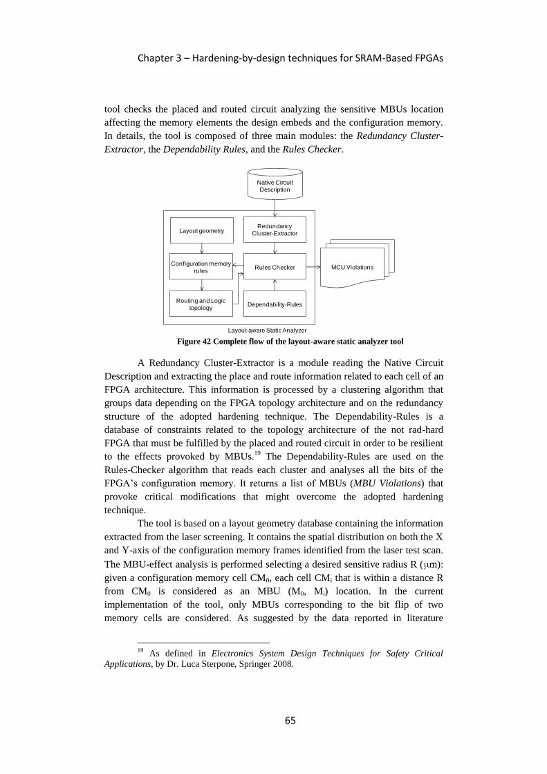
Chapter 3 – Hardening-by-design techniques for SRAM-Based FPGAs
65
tool checks the placed and routed circuit analyzing the sensitive MBUs location
affecting the memory elements the design embeds and the configuration memory.
In details, the tool is composed of three main modules: the Redundancy Cluster-
Extractor, the Dependability Rules, and the Rules Checker.
Figure 42 Complete flow of the layout-aware static analyzer tool
A Redundancy Cluster-Extractor is a module reading the Native Circuit
Description and extracting the place and route information related to each cell of an
FPGA architecture. This information is processed by a clustering algorithm that
groups data depending on the FPGA topology architecture and on the redundancy
structure of the adopted hardening technique. The Dependability-Rules is a
database of constraints related to the topology architecture of the not rad-hard
FPGA that must be fulfilled by the placed and routed circuit in order to be resilient
to the effects provoked by MBUs.19
The Dependability-Rules are used on the
Rules-Checker algorithm that reads each cluster and analyses all the bits of the
FPGA’s configuration memory. It returns a list of MBUs (MBU Violations) that
provoke critical modifications that might overcome the adopted hardening
technique.
The tool is based on a layout geometry database containing the information
extracted from the laser screening. It contains the spatial distribution on both the X
and Y-axis of the configuration memory frames identified from the laser test scan.
The MBU-effect analysis is performed selecting a desired sensitive radius R ( m):
given a configuration memory cell CM0, each cell CMi that is within a distance R
from CM0 is considered as an MBU (M0, Mi) location. In the current
implementation of the tool, only MBUs corresponding to the bit flip of two
memory cells are considered. As suggested by the data reported in literature
19 As defined in Electronics System Design Techniques for Safety Critical
Applications, by Dr. Luca Sterpone, Springer 2008.
Layout-aware Static Analyzer
Dependability-Rules
Redundancy
Cluster-Extractor
Rules Checker
Native Circuit
Description
MCU Violations
Routing and Logic
topology
Configuration memory
rules
Layout geometry
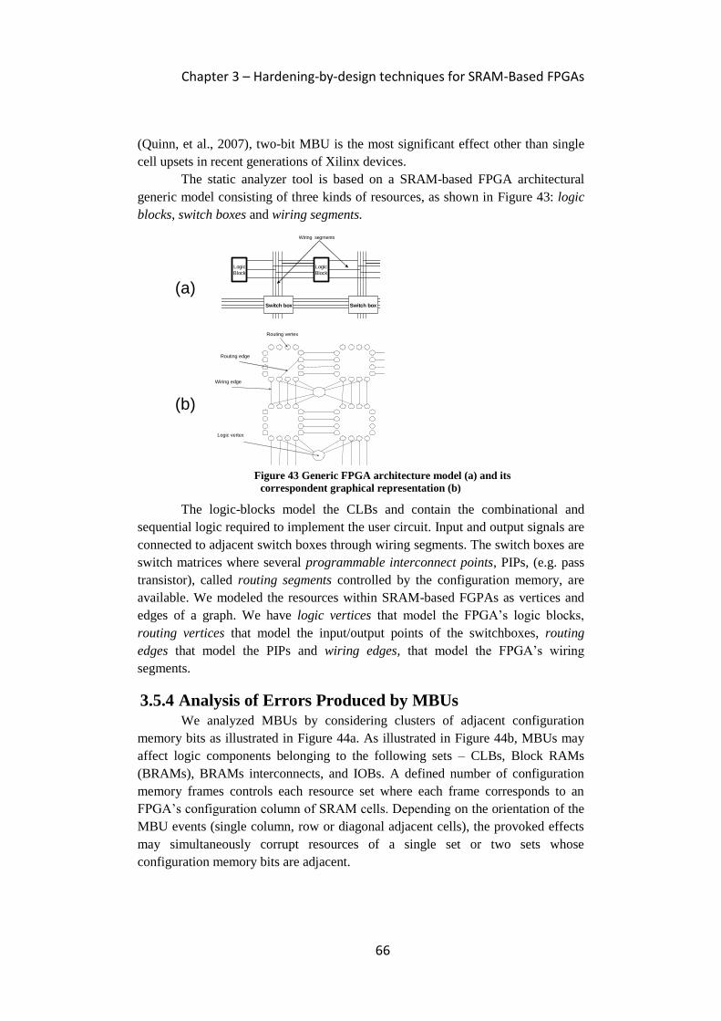
Chapter 3 – Hardening-by-design techniques for SRAM-Based FPGAs
66
(Quinn, et al., 2007), two-bit MBU is the most significant effect other than single
cell upsets in recent generations of Xilinx devices.
The static analyzer tool is based on a SRAM-based FPGA architectural
generic model consisting of three kinds of resources, as shown in Figure 43: logic
blocks, switch boxes and wiring segments.
The logic-blocks model the CLBs and contain the combinational and
sequential logic required to implement the user circuit. Input and output signals are
connected to adjacent switch boxes through wiring segments. The switch boxes are
switch matrices where several programmable interconnect points, PIPs, (e.g. pass
transistor), called routing segments controlled by the configuration memory, are
available. We modeled the resources within SRAM-based FGPAs as vertices and
edges of a graph. We have logic vertices that model the FPGA’s logic blocks,
routing vertices that model the input/output points of the switchboxes, routing
edges that model the PIPs and wiring edges, that model the FPGA’s wiring
segments.
3.5.4 Analysis of Errors Produced by MBUs We analyzed MBUs by considering clusters of adjacent configuration
memory bits as illustrated in Figure 44a. As illustrated in Figure 44b, MBUs may
affect logic components belonging to the following sets – CLBs, Block RAMs
(BRAMs), BRAMs interconnects, and IOBs. A defined number of configuration
memory frames controls each resource set where each frame corresponds to an
FPGA’s configuration column of SRAM cells. Depending on the orientation of the
MBU events (single column, row or diagonal adjacent cells), the provoked effects
may simultaneously corrupt resources of a single set or two sets whose
configuration memory bits are adjacent.
Wiring segments
Switch box
Switch box
Switch box
Switch box
Logic
Block
Logic
Block
Logic
Block
Logic
Block
Logic
Block
Logic
Block
Logic
Block
Logic
Block
Logic
Block
Switch box
Switch box
Logic
Block
Logic
Block
Logic
Block
Routing vertex
Routing edge
Wiring edge
Logic vertex
(a)
(b)
Figure 43 Generic FPGA architecture model (a) and its
correspondent graphical representation (b)
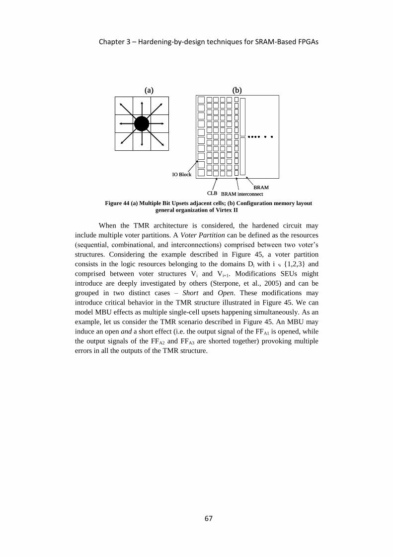
Chapter 3 – Hardening-by-design techniques for SRAM-Based FPGAs
67
Figure 44 (a) Multiple Bit Upsets adjacent cells; (b) Configuration memory layout
general organization of Virtex II
When the TMR architecture is considered, the hardened circuit may
include multiple voter partitions. A Voter Partition can be defined as the resources
(sequential, combinational, and interconnections) comprised between two voter’s
structures. Considering the example described in Figure 45, a voter partition
consists in the logic resources belonging to the domains Di with i {1,2,3} and
comprised between voter structures Vi and Vi+1. Modifications SEUs might
introduce are deeply investigated by others (Sterpone, et al., 2005) and can be
grouped in two distinct cases – Short and Open. These modifications may
introduce critical behavior in the TMR structure illustrated in Figure 45. We can
model MBU effects as multiple single-cell upsets happening simultaneously. As an
example, let us consider the TMR scenario described in Figure 45. An MBU may
induce an open and a short effect (i.e. the output signal of the FFA1 is opened, while
the output signals of the FFA2 and FFA3 are shorted together) provoking multiple
errors in all the outputs of the TMR structure.
(a)
IO Block
CLB BRAM interconnect
BRAM
(b)(a)
IO Block
CLB BRAM interconnect
BRAM
(b)
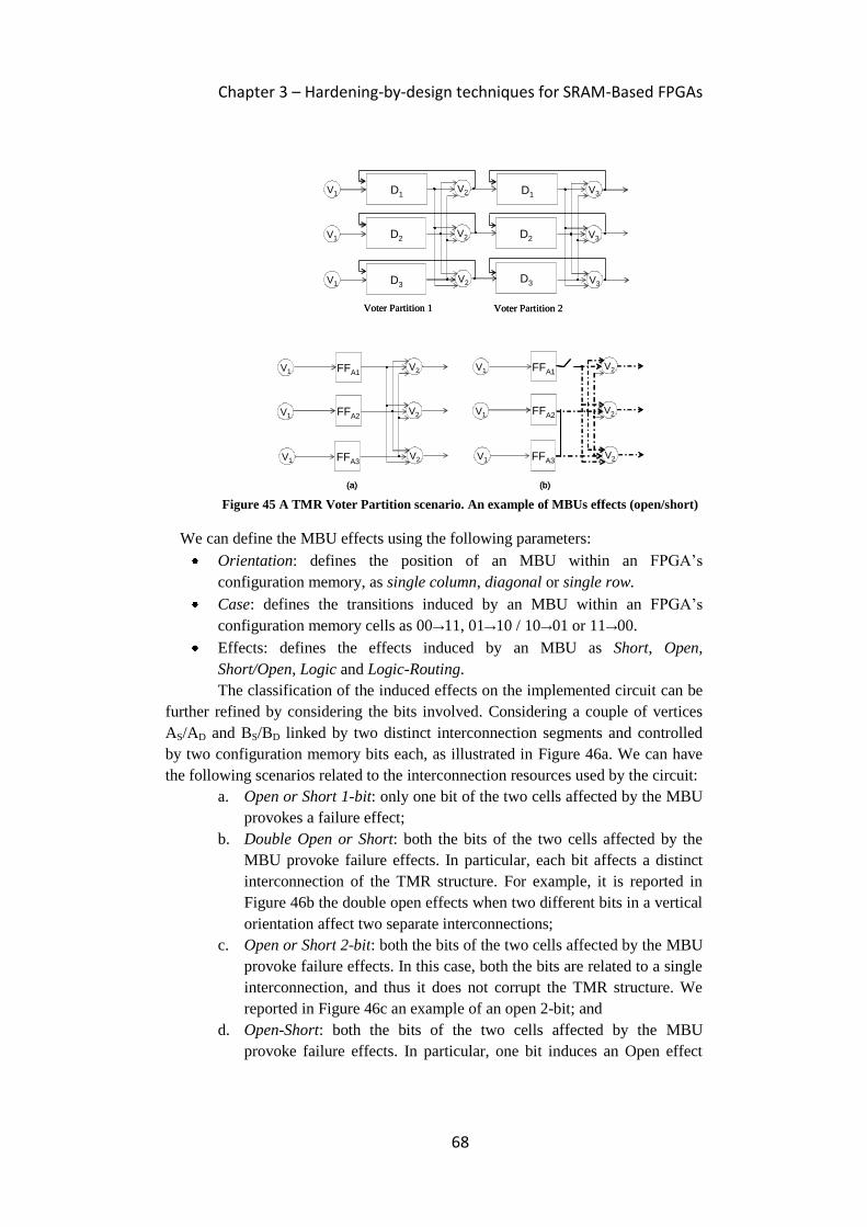
Chapter 3 – Hardening-by-design techniques for SRAM-Based FPGAs
68
Figure 45 A TMR Voter Partition scenario. An example of MBUs effects (open/short)
We can define the MBU effects using the following parameters:
Orientation: defines the position of an MBU within an FPGA’s
configuration memory, as single column, diagonal or single row.
Case: defines the transitions induced by an MBU within an FPGA’s
configuration memory cells as 00→11, 01→10 / 10→01 or 11→00.
Effects: defines the effects induced by an MBU as Short, Open,
Short/Open, Logic and Logic-Routing.
The classification of the induced effects on the implemented circuit can be
further refined by considering the bits involved. Considering a couple of vertices
AS/AD and BS/BD linked by two distinct interconnection segments and controlled
by two configuration memory bits each, as illustrated in Figure 46a. We can have
the following scenarios related to the interconnection resources used by the circuit:
a. Open or Short 1-bit: only one bit of the two cells affected by the MBU
provokes a failure effect;
b. Double Open or Short: both the bits of the two cells affected by the
MBU provoke failure effects. In particular, each bit affects a distinct
interconnection of the TMR structure. For example, it is reported in
Figure 46b the double open effects when two different bits in a vertical
orientation affect two separate interconnections;
c. Open or Short 2-bit: both the bits of the two cells affected by the MBU
provoke failure effects. In this case, both the bits are related to a single
interconnection, and thus it does not corrupt the TMR structure. We
reported in Figure 46c an example of an open 2-bit; and
d. Open-Short: both the bits of the two cells affected by the MBU
provoke failure effects. In particular, one bit induces an Open effect
D1V3
V3
V3
V2
V2
V2
D1V1
V1
V1
Voter Partition 1 Voter Partition 2
D2 D2
D3D3
D1V3
V3
V3
V2
V2
V2
D1V1
V1
V1
Voter Partition 1 Voter Partition 2
D2 D2
D3D3
(a) (b)
V2
V2
V2
FFA1V1
V1
V1
FFA2
FFA3
V2
V2
V2
FFA1V1
V1
V1
FFA2
FFA3
(a) (b)
V2
V2
V2
FFA1V1
V1
V1
FFA2
FFA3
V2
V2
V2
FFA1V1
V1
V1
FFA2
FFA3
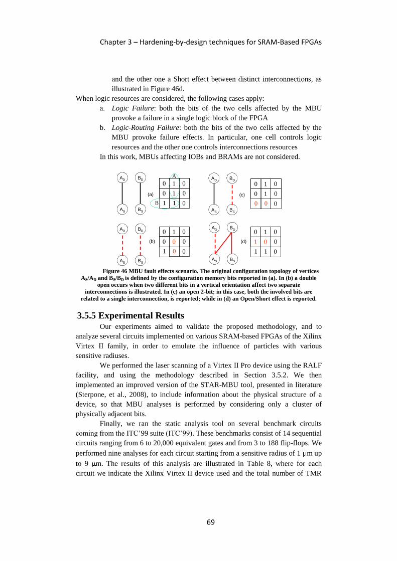
Chapter 3 – Hardening-by-design techniques for SRAM-Based FPGAs
69
and the other one a Short effect between distinct interconnections, as
illustrated in Figure 46d.
When logic resources are considered, the following cases apply:
a. Logic Failure: both the bits of the two cells affected by the MBU
provoke a failure in a single logic block of the FPGA
b. Logic-Routing Failure: both the bits of the two cells affected by the
MBU provoke failure effects. In particular, one cell controls logic
resources and the other one controls interconnections resources
In this work, MBUs affecting IOBs and BRAMs are not considered.
Figure 46 MBU fault effects scenario. The original configuration topology of vertices
AS/AD and BS/BD is defined by the configuration memory bits reported in (a). In (b) a double
open occurs when two different bits in a vertical orientation affect two separate
interconnections is illustrated. In (c) an open 2-bit; in this case, both the involved bits are
related to a single interconnection, is reported; while in (d) an Open/Short effect is reported.
3.5.5 Experimental Results Our experiments aimed to validate the proposed methodology, and to
analyze several circuits implemented on various SRAM-based FPGAs of the Xilinx
Virtex II family, in order to emulate the influence of particles with various
sensitive radiuses.
We performed the laser scanning of a Virtex II Pro device using the RALF
facility, and using the methodology described in Section 3.5.2. We then
implemented an improved version of the STAR-MBU tool, presented in literature
(Sterpone, et al., 2008), to include information about the physical structure of a
device, so that MBU analyses is performed by considering only a cluster of
physically adjacent bits.
Finally, we ran the static analysis tool on several benchmark circuits
coming from the ITC’99 suite (ITC’99). These benchmarks consist of 14 sequential
circuits ranging from 6 to 20,000 equivalent gates and from 3 to 188 flip-flops. We
performed nine analyses for each circuit starting from a sensitive radius of 1 m up
to 9 m. The results of this analysis are illustrated in Table 8, where for each
circuit we indicate the Xilinx Virtex II device used and the total number of TMR
AD
AS
BD
BS
AD
AS
BD
BS
AD
AS
BD
BS
(a)
(b)
1
1
11
0
0
0
0
0
1
0
01
0
0
0
0
0
AD
AS
BD
BS
(c)
1
1
00
0
0
0
0
0
A
B
(d)
1
0
11
0
1
0
0
0

Chapter 3 – Hardening-by-design techniques for SRAM-Based FPGAs
70
failures due to double-cells MBUs for each sensitive radius considered. The
distribution of the sensitiveness related to the benchmark circuit B14 is also
illustrated in Figure 47. This is the most complex benchmark we considered, and it
consists of a subset of the VIPER20
microprocessor.
Figure 47 Total Multiple Bit Upsets distribution on benchmark circuit B14 with
respect to a sensitive radius contained between 1 and 9 µm
Device Circuits
Total TMR Failure
Sensitive radius [ m]
1 2 3 4 5 6 7 8 9
XC2V40 B01 5 14 18 20 20 21 21 21 21
XC2V40 B02 5 12 13 13 16 16 16 16 16
XC2V40 B03 18 57 69 74 79 79 79 79 80
XC2V40 B04 362 1,104 1,139 1,166 1,292 1,292 1,362 1,397 1,460
XC2V80 B05 396 1,260 1,359 1,400 1,498 1,498 1,579 1,632 1,715
XC2V40 B06 7 23 23 23 27 27 31 31 31
XC2V40 B07 183 577 635 647 686 686 711 730 767
XC2V40 B08 14 39 39 41 54 54 54 56 57
XC2V40 B09 12 42 45 45 57 57 60 60 61
XC2V40 B10 45 152 164 170 180 180 196 196 206
XC2V40 B11 492 1,481 1,601 1,639 1,746 1,746 1,801 1,847 1,924
XC2V250 B12 57 178 197 217 217 217 227 238 253
XC2V40 B13 340 1,113 1,189 1,208 1,293 1,293 1,345 1,404 1,455
XC2V1500 B14 8,759 26,712 28,539 29,252 30,809 30,809 32,238 32,764 34,776
Table 8 Total double MBU effects on X-TMR circuits
It is possible to notice that TMR failures follow a logarithmic distribution,
which drastically increases, between 1 m and 2 m. This growth is due to the
threshold distance between the rows of each frame (i.e. when the sensitive radius is
smaller than 2 m, the identified silicon area does not contains two configuration
20
VIPER, Verifiable Integrated Processor for Enhanced Reliability, is a 32-bit
microprocessor architecture designed by the Royal Signals and Radar Establishment in
Malvern, United Kingdom.
0
5000
10000
15000
20000
25000
30000
35000
40000
1 2 3 4 5 6 7 8 9
To
tal T
MR
Failu
re
Sensitive radius [ m]
TMR Failure / Sensitive radius B14 benchmark

Chapter 3 – Hardening-by-design techniques for SRAM-Based FPGAs
71
memory cells). When radiuses larger than the threshold distance are considered, the
TMR failures increase constantly.
As Multiple Bit Upset effects are becoming increasingly more important, a
growing interest is expected for including device-specific layout information into
analysis tools supporting designers in developing critical circuits on SRAM-based
FPGAs. This kind of information is normally unavailable to FPGA end-users, and
therefore to the best of our knowledge until now, analysis tools like static analyzers
as well as fault injection tools supported only partially MBUs.
In this work, we proposed a methodology to first derive layout information
by characterizing the FPGA device of choice using laser testing. The gathered
information is then used to guide a static analysis tool in investigating multiple
effects. Experimental results gathered on several benchmark circuits show the
capabilities of this methodology. To refine this methodology, a set of radiation
testing experiments is envisioned, to estimate the average value for the sensitive
radius for a device considered, versus the particle LET, to provide designers with a
complete solution to assess the impact of multiple bit upsets in their designs.

73
Chapter 4
Radiation effects on Flash-based
FPGAs
Flash-based FPGAs are becoming an attractive solution for the space
exploration community because their configuration memory is unaffected by
Single Event Upsets, SEUs as in SRAM-based FPGAs. User memory in this kind
of device (i.e. flip-flops and embedded SRAM) is still affected by single event
upsets, but designers can cope with this problem using redundancy and error
correction codes. In this scenario Single Event Transient, SET, effects become the
major critical issue. Indeed, radiation can induce voltage glitches in combinatorial
logic that could propagate to memory elements, and if latched, these glitches could
lead to single or multiple errors (depending of the fan-out of the affected logic).
Furthermore, these kinds of events can affect global circuit lines, such as clock and
reset, leading to whole or partial circuit failures. It is important to understand the
impact of several possible effects on a design, defining the corresponding criticality
level and identifying the impact circuit-parameters have on the overall design
sensitiveness. Our studies target Actel devices; in particular, we tested devices of
the ProASIC3 family, manufactured in a 130 nm CMOS process. All the presented
work is the result of collaboration with the Politecnico di Torino.
4.1 Flash-based FPGAs architecture
As presented in Figure 48, the basic FPGA architecture is composed of an
array of logic cells, called VersaTiles21
, I/O blocks and embedded SRAM. Their
reconfiguration capability is obtained by means of a Flash switch (Speers, et al.,
1999). Two devices make up this element (Figure 49):
21
In the Actel nomenclature
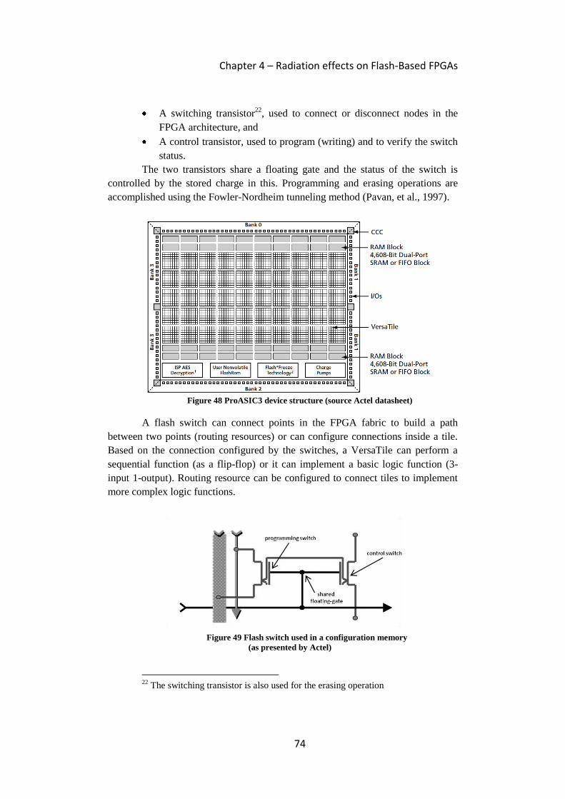
Chapter 4 – Radiation effects on Flash-Based FPGAs
74
A switching transistor22
, used to connect or disconnect nodes in the
FPGA architecture, and
A control transistor, used to program (writing) and to verify the switch
status.
The two transistors share a floating gate and the status of the switch is
controlled by the stored charge in this. Programming and erasing operations are
accomplished using the Fowler-Nordheim tunneling method (Pavan, et al., 1997).
Figure 48 ProASIC3 device structure (source Actel datasheet)
A flash switch can connect points in the FPGA fabric to build a path
between two points (routing resources) or can configure connections inside a tile.
Based on the connection configured by the switches, a VersaTile can perform a
sequential function (as a flip-flop) or it can implement a basic logic function (3-
input 1-output). Routing resource can be configured to connect tiles to implement
more complex logic functions.
22
The switching transistor is also used for the erasing operation
Figure 49 Flash switch used in a configuration memory
(as presented by Actel)
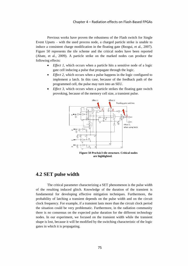
Chapter 4 – Radiation effects on Flash-Based FPGAs
75
Previous works have proven the robustness of the Flash switch for Single
Event Upsets – with the used process node, a charged particle strike is unable to
induce a consistent charge modification in the floating gate (Rezgui, et al., 2007).
Figure 50 represents the tile scheme and the critical nodes have been reported
(Abate, et al., 2009). A particle strike on the marked nodes can produce the
following effects:
Effect 1, which occurs when a particle hits a sensitive node of a logic
gate cell inducing a pulse that propagate through the logic.
Effect 2, which occurs when a pulse happens in the logic configured to
implement a latch. In this case, because of the feedback path of the
programmed cell, the pulse may turn into an SEU.
Effect 3, which occurs when a particle strikes the floating gate switch
provoking, because of the memory cell size, a transient pulse.
4.2 SET pulse width
The critical parameter characterizing a SET phenomenon is the pulse width
of the resulting induced glitch. Knowledge of the duration of the transient is
fundamental for developing effective mitigation techniques. Furthermore, the
probability of latching a transient depends on the pulse width and on the circuit
clock frequency. For example, if a transient lasts more than the circuit clock period
the situation could be very problematic. Furthermore, in the radiation community
there is no consensus on the expected pulse duration for the different technology
nodes. In our experiment, we focused on the transient width while the transient
shape is lost, because it will be modified by the switching characteristic of the logic
gates in which it is propagating.
Figure 50 ProAsic3 tile structure. Critical nodes
are highlighted.
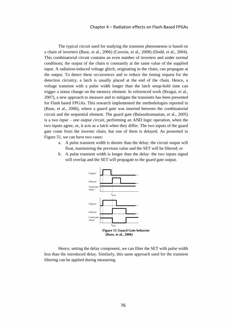
Chapter 4 – Radiation effects on Flash-Based FPGAs
76
The typical circuit used for studying the transient phenomenon is based on
a chain of inverters (Baze, et al., 2006) (Cavrois, et al., 2008) (Dodd, et al., 2004).
This combinatorial circuit contains an even number of inverters and under normal
conditions; the output of the chain is constantly at the same value of the supplied
input. A radiation-induced voltage glitch, originating in the chain, can propagate at
the output. To detect these occurrences and to reduce the timing request for the
detection circuitry, a latch is usually placed at the end of the chain. Hence, a
voltage transient with a pulse width longer than the latch setup-hold time can
trigger a status change on the memory element. In referenced work (Rezgui, et al.,
2007), a new approach to measure and to mitigate the transients has been presented
for Flash based FPGAs. This research implemented the methodologies reported in
(Baze, et al., 2006), where a guard gate was inserted between the combinatorial
circuit and the sequential element. The guard gate (Balasubramanian, et al., 2005)
is a two input – one output circuit, performing an AND logic operation, when the
two inputs agree, or, it acts as a latch when they differ. The two inputs of the guard
gate come from the inverter chain, but one of them is delayed. As presented in
Figure 51, we can have two cases:
a. A pulse transient width is shorter than the delay: the circuit output will
float, maintaining the previous value and the SET will be filtered; or
b. A pulse transient width is longer than the delay: the two inputs signal
will overlap and the SET will propagate to the guard gate output.
Hence, setting the delay component, we can filter the SET with pulse width
less than the introduced delay. Similarly, this same approach used for the transient
filtering can be applied during measuring.
Figure 51 Guard Gate behavior
(Baze, et al., 2006)

Chapter 4 – Radiation effects on Flash-Based FPGAs
77
4.2.1 Experimental setup for SET pulse width measurement We built-up an experimental setup for studying the induced SETs under
heavy-ion beam irradiation. As shown in Figure 52, our test setup included:
a. Device Under Test, DUT: Actel ProASIC3, hosted in an evaluation
board;
b. Monitoring Device, MD: a circuit was implemented on a Xilinx FPGA
performing the monitoring of the DUT outputs; and
c. Logging PC: a computer connected via JTAG to the MD, acts as
experiment controller and logs all events detected.
Connections between the DUT and the MD are achieved by means of
twisted-pair cables, in order to reduce electromagnetic noise. The PC is connected
to the MD through the JTAG port on the board. This allows initializing of the
board and downloading the experiment’s results. These results are stored in some
registers of the device; the PC can obtain the date by performing a simple readback
operation, i.e. reading the content of the MD configuration memory23
.
4.2.1.1 The DUT design
In order to study the effects of transient faults on Flash-based FPGAs, we
implemented in the DUT an ad-hoc circuit that maximizes the probability of
capturing transient events and making them observable to the monitoring device. A
chain of inverter gates occupies almost the whole of the device resources, allowing
capture of the majority of SETs induced by the ion beam. During irradiation tests,
it is possible to detect transient faults by means of a static test; in particular, the
chain input is held at ‘0’. To detect radiation effects, it is enough to implement a
‘1’s recognizer that observes the end of the chain.
23
The FPGA readback is performed using the JTAG interface.
Figure 52 Setup used to study the SET
pulse width schematic.

Chapter 4 – Radiation effects on Flash-Based FPGAs
78
To measure SET width, we considered several points on the chain,
separated by an even number of inverters. In this manner, all of them represent the
same signal at different times. Observing the value at the end of the chain and the
value at one of these points, it is possible to detect an SET on both signals at the
same time if and only if its width is greater than the delay between the two signals
(∆T). If both assume a high value at the same time, an SET is detected. Figure 53
shows a scheme of the radiated design implemented in the DUT, where ∆0 is the
signal at the end of the chain, with no delay, and ∆i is the generic i signal with an
incremental delay of i·∆T with respect to the chain’s end.
The comparator is implemented with a guard-gate that lets the SETs pass
only if both ∆0 and ∆i channels are high at the same time; otherwise it keeps the
last output value. A SET passes only if it is longer than i·∆T; otherwise the guard
gate masks the fault. Working the MD at a frequency presumably lower than 1
GHz, in order to observe SETs of the order of a few ns, a strategy to allow the
sampling is needed. This architecture has been called keeping mechanism. For this
reason, a latch is added at the end of every channel. However, the introduction of a
latch leads to further issues due to it being sensitive to radiation, and, in particular,
a bit-flip can induce false event detection. Therefore, the Triple Modular
Redundancy, TMR, technique has been adopted to protect the keeping mechanism
from radiation-induced upsets. Every latch is tripled and the outputs of the replicas
are voted, in order to avoid a faulty latch to induce a false SET count. Because also
the voting mechanism can be affected by radiation, it is placed in the monitoring
FPGA, thus requiring the outputs of the DUT to be tripled. Latches are then reset
as soon as the MD has recognized the SET. Figure 54 details the guard gate
structure as well as the keeping mechanism and the application of the TMR
technique. Considering the input/output structure of the DUT, different signals on
the same I/O bank can be affected by a fault produced by a single particle, thus
Figure 53 Device Under Test design. A long chain of
inverters has been implemented in an Actel ProAsic3 FPGA. The
circuit occupies almost the whole device. SETs are measured at
different point of the chain.
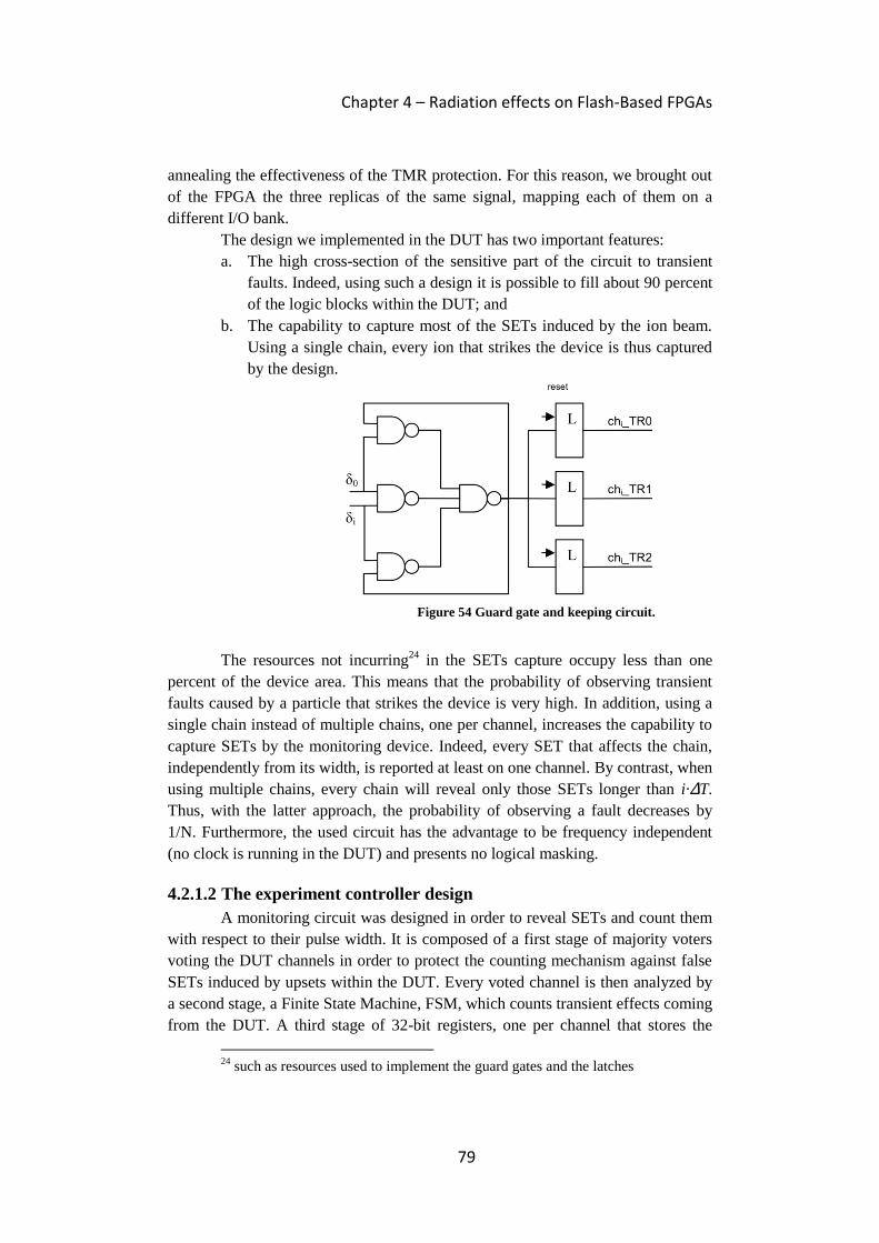
Chapter 4 – Radiation effects on Flash-Based FPGAs
79
annealing the effectiveness of the TMR protection. For this reason, we brought out
of the FPGA the three replicas of the same signal, mapping each of them on a
different I/O bank.
The design we implemented in the DUT has two important features:
a. The high cross-section of the sensitive part of the circuit to transient
faults. Indeed, using such a design it is possible to fill about 90 percent
of the logic blocks within the DUT; and
b. The capability to capture most of the SETs induced by the ion beam.
Using a single chain, every ion that strikes the device is thus captured
by the design.
The resources not incurring24
in the SETs capture occupy less than one
percent of the device area. This means that the probability of observing transient
faults caused by a particle that strikes the device is very high. In addition, using a
single chain instead of multiple chains, one per channel, increases the capability to
capture SETs by the monitoring device. Indeed, every SET that affects the chain,
independently from its width, is reported at least on one channel. By contrast, when
using multiple chains, every chain will reveal only those SETs longer than i·∆T.
Thus, with the latter approach, the probability of observing a fault decreases by
1/N. Furthermore, the used circuit has the advantage to be frequency independent
(no clock is running in the DUT) and presents no logical masking.
4.2.1.2 The experiment controller design
A monitoring circuit was designed in order to reveal SETs and count them
with respect to their pulse width. It is composed of a first stage of majority voters
voting the DUT channels in order to protect the counting mechanism against false
SETs induced by upsets within the DUT. Every voted channel is then analyzed by
a second stage, a Finite State Machine, FSM, which counts transient effects coming
from the DUT. A third stage of 32-bit registers, one per channel that stores the
24
such as resources used to implement the guard gates and the latches
Figure 54 Guard gate and keeping circuit.

Chapter 4 – Radiation effects on Flash-Based FPGAs
80
counting information, follows the FSM. Finally, as soon as the FSM detects an
SET, it raises the reset signal for one clock cycle, in order to restore the initial
value of the DUT’s latches. Figure 55 depicts the architecture described above,
with the three stages of the DM.
The FSM counts SETs on the basis of a simple consideration – as
mentioned before, SETs induce a high value on every channel where i·∆T is less
than the pulse width; considering channel 0 acts like a flag that detects SETs,
unprotected by a guard gate, it is thus possible to recognize the SET’s width
discovering the first ‘0’ among channels from 1 to N. For example, if the SET’s
width is included between 3·∆T and 4·∆T, channel 0 will be ‘1’ and channels 1
through 3 will be at a high value, while channel 4 and subsequent will be at a low
value. The SET is then stored as belonging to channel 3.
Once the counting ends, the MD resets the DUT latches, in order to restore
their initial value. The counting process starts when the 0 channel detects an SET,
waits while the pulse is propagated through the last channel, then in a clock cycle
performs the counting and, finally, the FSM raises the reset signal for one clock
cycle. For this reason, the following SET that can be detected has to be N·∆T + 2
clock cycles – in nanoseconds – after its preceding one.
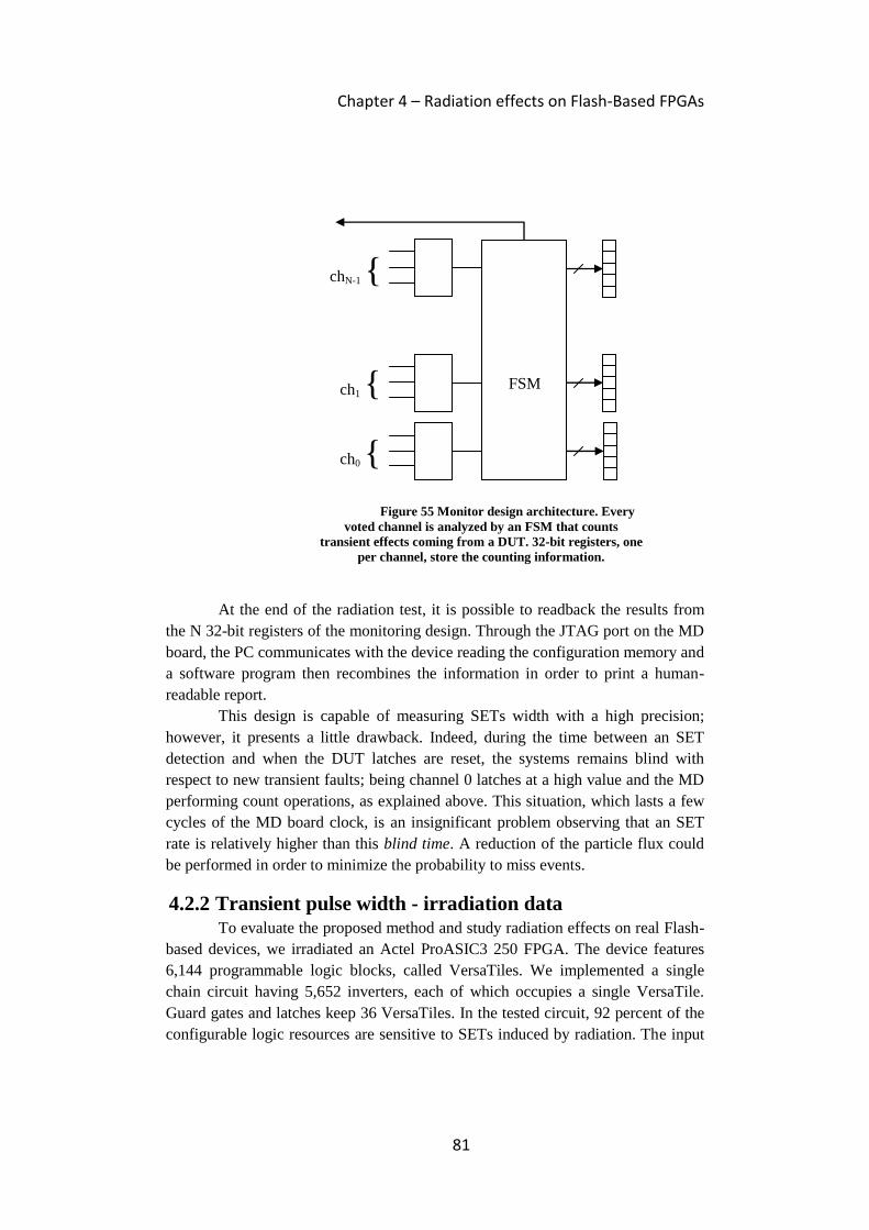
Chapter 4 – Radiation effects on Flash-Based FPGAs
81
At the end of the radiation test, it is possible to readback the results from
the N 32-bit registers of the monitoring design. Through the JTAG port on the MD
board, the PC communicates with the device reading the configuration memory and
a software program then recombines the information in order to print a human-
readable report.
This design is capable of measuring SETs width with a high precision;
however, it presents a little drawback. Indeed, during the time between an SET
detection and when the DUT latches are reset, the systems remains blind with
respect to new transient faults; being channel 0 latches at a high value and the MD
performing count operations, as explained above. This situation, which lasts a few
cycles of the MD board clock, is an insignificant problem observing that an SET
rate is relatively higher than this blind time. A reduction of the particle flux could
be performed in order to minimize the probability to miss events.
4.2.2 Transient pulse width - irradiation data To evaluate the proposed method and study radiation effects on real Flash-
based devices, we irradiated an Actel ProASIC3 250 FPGA. The device features
6,144 programmable logic blocks, called VersaTiles. We implemented a single
chain circuit having 5,652 inverters, each of which occupies a single VersaTile.
Guard gates and latches keep 36 VersaTiles. In the tested circuit, 92 percent of the
configurable logic resources are sensitive to SETs induced by radiation. The input
v
V
V
ch1 {
ch0 {
chN-1 { 3
2
3
2
3
2
FSM
Figure 55 Monitor design architecture. Every
voted channel is analyzed by an FSM that counts
transient effects coming from a DUT. 32-bit registers, one
per channel, store the counting information.
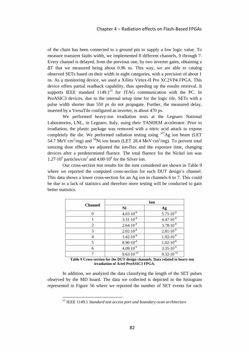
Chapter 4 – Radiation effects on Flash-Based FPGAs
82
of the chain has been connected to a ground pin to supply a low logic value. To
measure transient faults width, we implemented 8 different channels, 0 through 7.
Every channel is delayed, from the previous one, by two inverter gates, obtaining a
∆T that we measured being about 0.96 ns. This way, we are able to catalog
observed SETs based on their width in eight categories, with a precision of about 1
ns. As a monitoring device, we used a Xilinx Virtex-II Pro XC2VP4 FPGA. This
device offers partial readback capability, thus speeding up the results retrieval. It
supports IEEE standard 1149.125
for JTAG communication with the PC. In
ProASIC3 devices, due to the internal setup time for the logic tile, SETs with a
pulse width shorter than 550 ps do not propagate. Further, the measured delay,
inserted by a VersaTile configured as inverter, is about 470 ps.
We performed heavy-ion irradiation tests at the Legnaro National
Laboratories, LNL, in Legnaro, Italy, using their TANDEM accelerator. Prior to
irradiation, the plastic package was removed with a nitric acid attack to expose
completely the die. We performed radiation testing using 107
Ag ion beam (LET
54.7 MeV·cm2/mg) and
58Ni ion beam (LET 28.4 MeV·cm
2/mg). To prevent total
ionizing dose effects we adjusted the ion-flux and the exposure time, changing
devices after a predetermined fluence. The total fluence for the Nickel ion was
1.27·106 particles/cm
2 and 4.00·10
6 for the Silver ion.
Our cross-section test results for the ions considered are shown in Table 9
where we reported the computed cross-section for each DUT design’s channel.
This data shows a lower cross-section for an Ag ion in channels 6 to 7. This could
be due to a lack of statistics and therefore more testing will be conducted to gain
better statistics.
Channel Ion
Ni Ag
0 4.03 10-8
5.75 10-8
1 3.31 10-8
4.47 10-8
2 2.64 10-8
3.78 10-8
3 2.02 10-8
2.81 10-8
4 1.42 10-8
1.92 10-8
5 8.90 10-8
1.02 10-8
6 4.09 10-9
3.35 10-9
7 9.63 10-10
9.32 10-10
Table 9 Cross-section for the DUT design channels. Data related to heavy-ion
irradiation of Actel ProASIC3 FPGA.
In addition, we analyzed the data classifying the length of the SET pulses
observed by the MD board. The data we collected is depicted in the histogram
represented in Figure 56 where we reported the number of SET events for each
25 IEEE 1149.1 Standard test access port and boundary-scan architecture
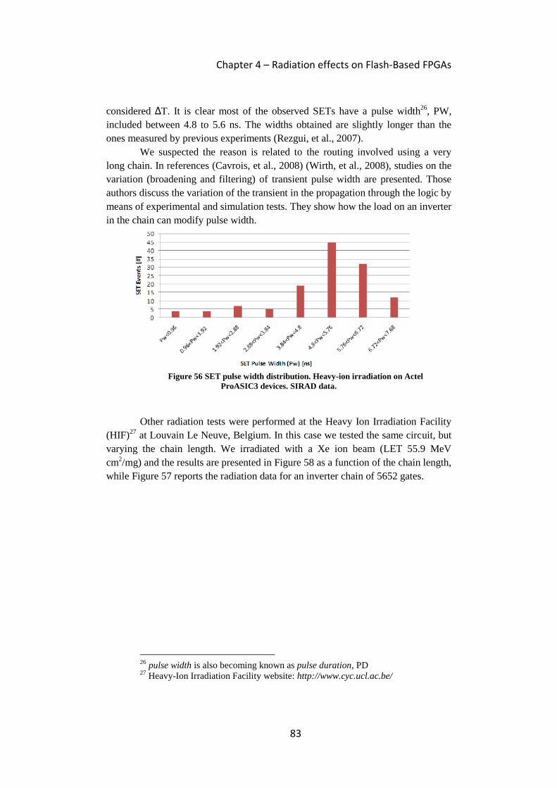
Chapter 4 – Radiation effects on Flash-Based FPGAs
83
considered ∆T. It is clear most of the observed SETs have a pulse width26
, PW,
included between 4.8 to 5.6 ns. The widths obtained are slightly longer than the
ones measured by previous experiments (Rezgui, et al., 2007).
We suspected the reason is related to the routing involved using a very
long chain. In references (Cavrois, et al., 2008) (Wirth, et al., 2008), studies on the
variation (broadening and filtering) of transient pulse width are presented. Those
authors discuss the variation of the transient in the propagation through the logic by
means of experimental and simulation tests. They show how the load on an inverter
in the chain can modify pulse width.
Figure 56 SET pulse width distribution. Heavy-ion irradiation on Actel
ProASIC3 devices. SIRAD data.
Other radiation tests were performed at the Heavy Ion Irradiation Facility
(HIF)27
at Louvain Le Neuve, Belgium. In this case we tested the same circuit, but
varying the chain length. We irradiated with a Xe ion beam (LET 55.9 MeV
cm2/mg) and the results are presented in Figure 58 as a function of the chain length,
while Figure 57 reports the radiation data for an inverter chain of 5652 gates.
26 pulse width is also becoming known as pulse duration, PD 27
Heavy-Ion Irradiation Facility website: http://www.cyc.ucl.ac.be/
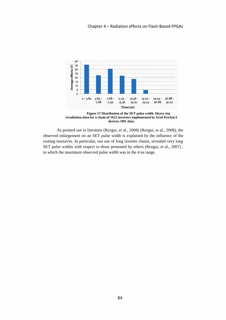
Chapter 4 – Radiation effects on Flash-Based FPGAs
84
As pointed out in literature (Rezgui, et al., 2008) (Rezgui, et al., 2008), the
observed enlargement on an SET pulse width is explained by the influence of the
routing resources. In particular, our use of long inverter chains, revealed very long
SET pulse widths with respect to those presented by others (Rezgui, et al., 2007) ,
in which the maximum observed pulse width was in the 4 ns range.
Figure 57 Distribution of the SET pulse width. Heavy-ion
irradiation data for a chain of 5652 inverters implemented in Actel ProAsic3
devices. HIF data.
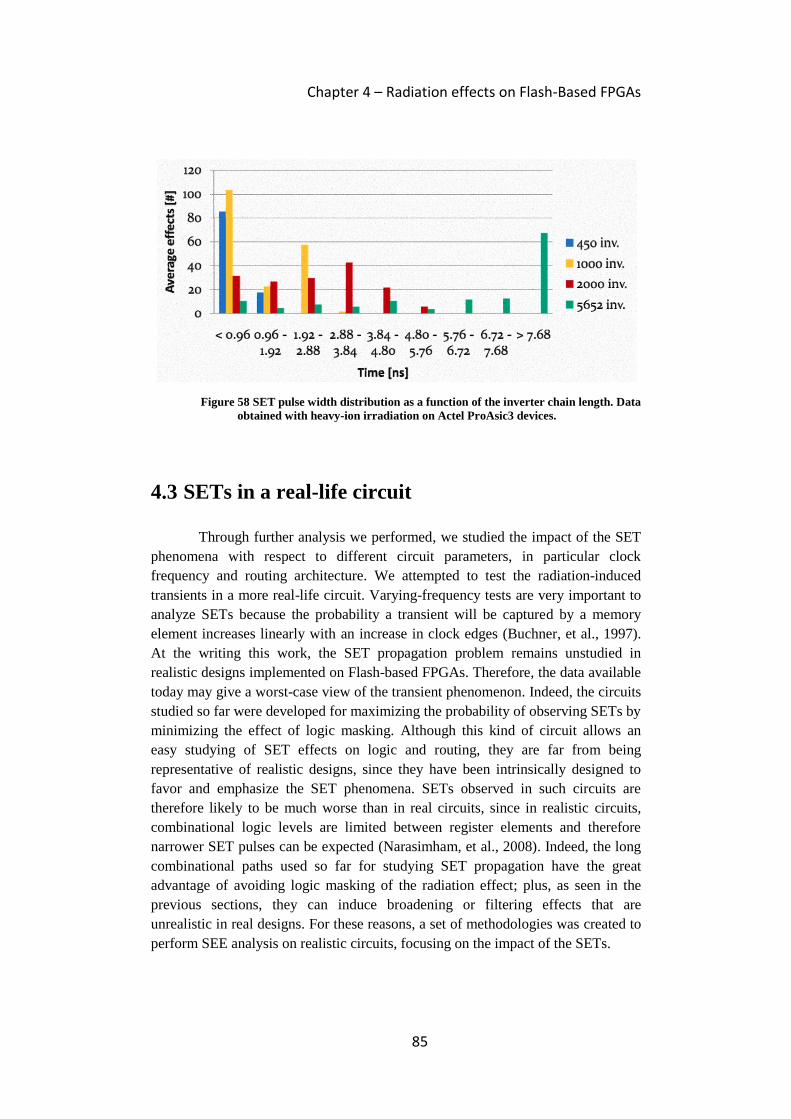
Chapter 4 – Radiation effects on Flash-Based FPGAs
85
4.3 SETs in a real-life circuit
Through further analysis we performed, we studied the impact of the SET
phenomena with respect to different circuit parameters, in particular clock
frequency and routing architecture. We attempted to test the radiation-induced
transients in a more real-life circuit. Varying-frequency tests are very important to
analyze SETs because the probability a transient will be captured by a memory
element increases linearly with an increase in clock edges (Buchner, et al., 1997).
At the writing this work, the SET propagation problem remains unstudied in
realistic designs implemented on Flash-based FPGAs. Therefore, the data available
today may give a worst-case view of the transient phenomenon. Indeed, the circuits
studied so far were developed for maximizing the probability of observing SETs by
minimizing the effect of logic masking. Although this kind of circuit allows an
easy studying of SET effects on logic and routing, they are far from being
representative of realistic designs, since they have been intrinsically designed to
favor and emphasize the SET phenomena. SETs observed in such circuits are
therefore likely to be much worse than in real circuits, since in realistic circuits,
combinational logic levels are limited between register elements and therefore
narrower SET pulses can be expected (Narasimham, et al., 2008). Indeed, the long
combinational paths used so far for studying SET propagation have the great
advantage of avoiding logic masking of the radiation effect; plus, as seen in the
previous sections, they can induce broadening or filtering effects that are
unrealistic in real designs. For these reasons, a set of methodologies was created to
perform SEE analysis on realistic circuits, focusing on the impact of the SETs.
Figure 58 SET pulse width distribution as a function of the inverter chain length. Data
obtained with heavy-ion irradiation on Actel ProAsic3 devices.

Chapter 4 – Radiation effects on Flash-Based FPGAs
86
Three different approaches have been used together in order to analyze
data from singular points of view and then combine them to provide single
consolidated pictures. On one platform, a flexible radiation-testing environment
was set-up to collect data from accelerated experiments, providing real-life-like
results. On another platform, two software-based techniques were partnered to
manage different circuit routing schemes and correlate them with radiation testing
data. First, a software tool replaces the circuit resources leaving their functionality
unchanged but modifying the routing; second, another tool analyses the FPGA
bitstream resulting from the previous transformation, computing the number of
sensitive programmable points that changed from the first version of the circuit.
4.3.1 Testing environment The testing environment we developed for evaluating SEE effects in Flash-
based FPGAs is a modification of the one used for studying the transient pulse
width. As illustrated in Figure 59, it is composed of three modules:
a hardware module hosting the Device Under Test, DUT;
a module with a Monitoring Device, MD; and
a Clock Generation Module, CGM.
Figure 59 Block diagram of the testing platform for heavy-ion
irradiation tests on Actel ProASIC3 devices.
The DUT is irradiated while operating at a clock frequency defined by the
CGM. In the meanwhile, the MD monitors the DUT outputs (channels) detecting
discrepancies in the functioning due to radiation-induced faults. The setup created
can be adapted to work with different DUT circuits. The design on the MD is a
general circuit that can monitor different events happening in the DUT according to
how the DUT is designed. The MD is able to count the events happening in the
DUT and store them into general-purpose registers that can be read by the software
running on the PC. In particular, the MD design is composed of a first stage of N
majority voters that vote the DUT output channels in order to protect the counting
mechanisms from false faults happening in the transmission stage between the
DUT and the MD. The maximum number of channels is defined by the maximum
number of data connections available between the DUT and the MD divided by 3,
because of output replication. Every voted channel is then analyzed by a second
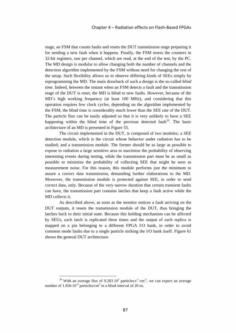
Chapter 4 – Radiation effects on Flash-Based FPGAs
87
stage, an FSM that counts faults and resets the DUT transmission stage preparing it
for sending a new fault when it happens. Finally, the FSM stores the counters in
32-bit registers, one per channel, which are read, at the end of the test, by the PC.
The MD design is modular to allow changing both the number of channels and the
detection algorithm implemented by the FSM without need for changing the rest of
the setup. Such flexibility allows us to observe differing kinds of SEEs simply by
reprogramming the MD. The main drawback of such a design is the so-called blind
time. Indeed, between the instant when an FSM detects a fault and the transmission
stage of the DUT is reset, the MD is blind to new faults. However, because of the
MD’s high working frequency (at least 100 MHz), and considering that this
operation requires few clock cycles, depending on the algorithm implemented by
the FSM, the blind time is considerably much lower than the SEE rate of the DUT.
The particle flux can be easily adjusted so that it is very unlikely to have a SEE
happening within the blind time of the previous detected fault28
. The basic
architecture of an MD is presented in Figure 55.
The circuit implemented in the DUT, is composed of two modules; a SEE
detection module, which is the circuit whose behavior under radiation has to be
studied; and a transmission module. The former should be as large as possible to
expose to radiation a large sensitive area to maximize the probability of observing
interesting events during testing, while the transmission part must be as small as
possible to minimize the probability of collecting SEE that might be seen as
measurement noise. For this reason, this module performs just the minimum to
assure a correct data transmission, demanding further elaborations to the MD.
Moreover, the transmission module is protected against SEE, in order to send
correct data, only. Because of the very narrow duration that certain transient faults
can have, the transmission part contains latches that keep a fault active while the
MD collects it.
As described above, as soon as the monitor notices a fault arriving on the
DUT outputs, it resets the transmission module of the DUT, thus bringing the
latches back to their initial state. Because this holding mechanism can be affected
by SEUs, each latch is replicated three times and the output of each replica is
mapped on a pin belonging to a different FPGA I/O bank, in order to avoid
common mode faults due to a single particle striking the I/O bank itself. Figure 61
shows the general DUT architecture.
28
With an average flux of 9.283 103 particles s
-1cm
-2, we can expect an average
number of 1.856 10-4
particles/cm2 in a blind interval of 20 ns.
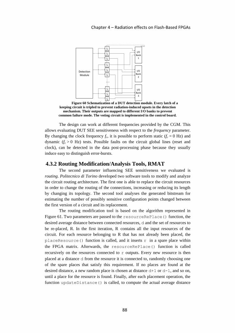
Chapter 4 – Radiation effects on Flash-Based FPGAs
88
Detection Module
L
L
L
L
L
L
L
L
L
. . .
I/OBank
1
I/OBank
2
I/OBank
3
reset
Figure 60 Schematization of a DUT detection module. Every latch of a
keeping circuit is tripled to prevent radiation-induced upsets in the detection
mechanism. Their outputs are mapped to different I/O banks to prevent
common failure mode. The voting circuit is implemented in the control board.
The design can work at different frequencies provided by the CGM. This
allows evaluating DUT SEE sensitiveness with respect to the frequency parameter.
By changing the clock frequency fc, it is possible to perform static (fc = 0 Hz) and
dynamic (fc > 0 Hz) tests. Possible faults on the circuit global lines (reset and
clock), can be detected in the data post-processing phase because they usually
induce easy to distinguish error-bursts.
4.3.2 Routing Modification/Analysis Tools, RMAT The second parameter influencing SEE sensitiveness we evaluated is
routing. Politecnico di Torino developed two software tools to modify and analyze
the circuit routing architecture. The first one is able to replace the circuit resources
in order to change the routing of the connections, increasing or reducing its length
by changing its topology. The second tool analyses the generated bitstream for
estimating the number of possibly sensitive configuration points changed between
the first version of a circuit and its replacement.
The routing modification tool is based on the algorithm represented in
Figure 61. Two parameters are passed to the resourceRePlace() function, the
desired average distance between connected resources, d and the set of resources to
be re-placed, R. In the first iteration, R contains all the input resources of the
circuit. For each resource belonging to R that has not already been placed, the
placeResource() function is called, and it inserts r in a spare place within
the FPGA matrix. Afterwards, the resourceRePlace() function is called
recursively on the resources connected to r outputs. Every new resource is then
placed at a distance d from the resource it is connected to, randomly choosing one
of the spare places that satisfy this requirement. If no places are found at the
desired distance, a new random place is chosen at distance d+1 or d-1, and so on,
until a place for the resource is found. Finally, after each placement operation, the
function updateDistance() is called, to compute the actual average distance

Chapter 4 – Radiation effects on Flash-Based FPGAs
89
δ. When all the resources have been correctly placed, the actual average distance is
returned.
The second software tool, developed by Politecnico di Torino, is a
bitstream analyzer, able to identify sensitive programmable points of a certain
FPGA design, i.e. configurable switches that can induce a fault if stricken by a
particle. Two steps compose the execution flow – the empty bitstream generation
and the circuit sensitiveness analysis. The first step consists in gathering
information about the bitstream structure of a certain device family. It is executed
only once per family and the information it provides are mandatory in order to
extract the circuit used resources (both routing and logic). The second step, instead,
analyses the design itself and provides a list of sensitive programmable points, and
is executed for every different circuit. Figure 62 shows such flow.
During the first step, the primary phase consists in generating the
‘discovery’ bitstream. A singular design is implemented, in order to discover the
bitstream structure and generate the necessary information to proceed to the second
step. This design consists in a unique spare gate (such as an inverter or an and gate)
that is simple enough to occupy a single tile of the whole device. Once the
discovery bitstream has been generated, the design is moved around the device area
in order to produce several copies of the same circuit with the only difference being
their location within the FPGA array. All these replicas are then compared, and
based on the regularity of the array architecture, and hypothetically, the bitstream
information, the tile location relationships and a bit positional mapping are
int resourceRePlace(int d, Set R)
{
static δ = 0;
for each (r in R){
if (r.unplaced == true){
placeResource (r, d);
δ = updateDistance();
}
δ = resourceRePlace(d,
r.outputs());
}
return δ;}
Figure 61 Routing modification algorithm used
by the RMAT tool

Chapter 4 – Radiation effects on Flash-Based FPGAs
90
produced. The location relationships define where the block of bits containing the
information related to a certain tile is located within the bitstream. Whereas, the bit
mapping describes where the bits related to a certain tile are, within the block.
Once the first step has been executed for the desired device, the output
information can be saved and reused for every design implemented in the same
family. The second step has to be executed for every design and analyses the SEE
sensitiveness of the implemented circuit, based on the output information of the
first step. In particular, for each device tile, the programmed bits are extracted by
the analyzer engine and they are cataloged according to their function using the
bitstream and resource rules generated by the first step. By now, the functions are
recognized between routing and logic. The first function identifies the bits involved
in routing elements, while the second one identifies the bits that program the logic
cells.
4.3.3 Experimental Setup According to the radiation test environment architecture described in the
previous section, we developed a SEE evaluation system based on two boards, the
first one hosting the Device Under Test, irradiated with heavy-ion beam, and the
second one monitoring the DUT outputs. In the DUT, we mapped a sequential
circuit implementing a multiplication between A and N, where A is the input of the
circuit and N is a number defined by the amount of pipeline stages of the circuit.
Every stage implements the addition between A and the result of the previous stage,
thus emulating the multiplication of A by i, where i is the number of the current
stage. A, an 8-bit wide, and the 9-th bits of the first-stage registers; are set to ‘0’
(carry input). In particular, A has been set to ‘0000001’, in order to minimize the
probability to have overflow, thus masking faults propagating toward the circuit
outputs. Such a circuit is more similar to a real design than the circuits used in any
Figure 62 Routing Analysis Tool workflow
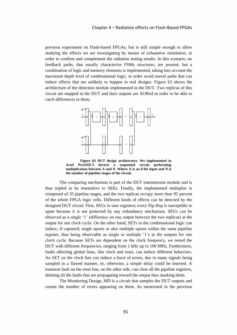
Chapter 4 – Radiation effects on Flash-Based FPGAs
91
previous experiment on Flash-based FPGAs, but is still simple enough to allow
studying the effects we are investigating by means of exhaustive simulation, in
order to confirm and complement the radiation testing results. In this scenario, no
feedback paths, that usually characterize FSMs structures, are present; but a
combination of logic and memory elements is implemented, taking into account the
maximum depth level of combinational logic, in order avoid unreal paths that can
induce effects that are unlikely to happen in real designs. Figure 63 shows the
architecture of the detection module implemented in the DUT. Two replicas of this
circuit are mapped in the DUT and their outputs are XORed in order to be able to
catch differences in them.
R
R
R
R
R
R
+ +. . .
. . .
R
R
R+8
8
9
Figure 63 DUT design architecture. We implemented in
Actel ProASIC3 devices a sequential circuit performing
multiplication between A and N. Where A is an 8-bit input and N is
the number of pipeline stages of the circuit.
The comparing mechanism is part of the DUT transmission module and is
thus tripled to be insensitive to SEEs. Finally, the implemented multiplier is
composed of 35 pipeline stages, and the two replicas occupy more than 95 percent
of the whole FPGA logic cells. Different kinds of effects can be detected by the
designed DUT circuit. First, SEUs in user registers; every flip-flop is susceptible to
upset because it is not protected by any redundancy mechanism. SEUs can be
observed as a single ‘1’ (difference on one output between the two replicas) at the
output for one clock cycle. On the other hand, SETs in the combinational logic can
induce, if captured; single upsets or also multiple upsets within the same pipeline
register, thus being observable as single or multiple ‘1’s at the outputs for one
clock cycle. Because SETs are dependent on the clock frequency, we tested the
DUT with different frequencies, ranging from 1 kHz up to 100 MHz. Furthermore,
faults affecting global lines, like clock and reset, can induce different behaviors.
An SET on the clock line can induce a burst of errors, due to many signals being
sampled in a flawed manner, or, otherwise, a simple delay could be inserted. A
transient fault on the reset line, on the other side, can clear all the pipeline registers,
deleting all the faults that are propagating toward the output thus masking them.
The Monitoring Design, MD is a circuit that samples the DUT outputs and
counts the number of errors appearing on them. As mentioned in the previous
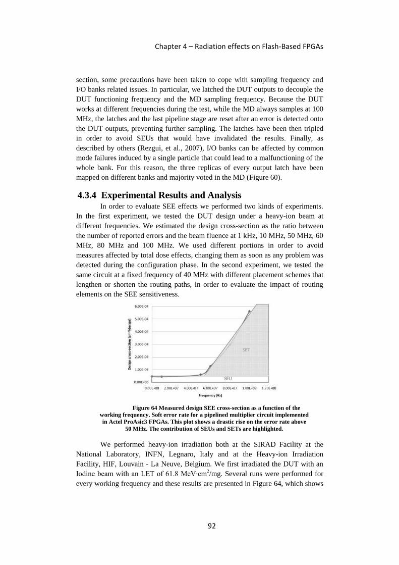
Chapter 4 – Radiation effects on Flash-Based FPGAs
92
section, some precautions have been taken to cope with sampling frequency and
I/O banks related issues. In particular, we latched the DUT outputs to decouple the
DUT functioning frequency and the MD sampling frequency. Because the DUT
works at different frequencies during the test, while the MD always samples at 100
MHz, the latches and the last pipeline stage are reset after an error is detected onto
the DUT outputs, preventing further sampling. The latches have been then tripled
in order to avoid SEUs that would have invalidated the results. Finally, as
described by others (Rezgui, et al., 2007), I/O banks can be affected by common
mode failures induced by a single particle that could lead to a malfunctioning of the
whole bank. For this reason, the three replicas of every output latch have been
mapped on different banks and majority voted in the MD (Figure 60).
4.3.4 Experimental Results and Analysis In order to evaluate SEE effects we performed two kinds of experiments.
In the first experiment, we tested the DUT design under a heavy-ion beam at
different frequencies. We estimated the design cross-section as the ratio between
the number of reported errors and the beam fluence at 1 kHz, 10 MHz, 50 MHz, 60
MHz, 80 MHz and 100 MHz. We used different portions in order to avoid
measures affected by total dose effects, changing them as soon as any problem was
detected during the configuration phase. In the second experiment, we tested the
same circuit at a fixed frequency of 40 MHz with different placement schemes that
lengthen or shorten the routing paths, in order to evaluate the impact of routing
elements on the SEE sensitiveness.
We performed heavy-ion irradiation both at the SIRAD Facility at the
National Laboratory, INFN, Legnaro, Italy and at the Heavy-ion Irradiation
Facility, HIF, Louvain - La Neuve, Belgium. We first irradiated the DUT with an
Iodine beam with an LET of 61.8 MeV∙cm2/mg. Several runs were performed for
every working frequency and these results are presented in Figure 64, which shows
Figure 64 Measured design SEE cross-section as a function of the
working frequency. Soft error rate for a pipelined multiplier circuit implemented
in Actel ProAsic3 FPGAs. This plot shows a drastic rise on the error rate above
50 MHz. The contribution of SEUs and SETs are highlighted.

Chapter 4 – Radiation effects on Flash-Based FPGAs
93
the design cross-section as a function of the working frequency. As one can
observe, up to 50 MHz, we observed no relevant variations on the error rate, thus
letting us think that below a certain frequency the cross-section is dominated by
SEUs affecting the user memory elements. For higher frequencies, we observed a
rapid increase of the error rate. In particular, at 100 MHz, it is about ten times the
error rate at 1 kHz, and the growth is concentrated between 50 to 100 MHz.
In the second experiment, we irradiated the DUT at a fixed frequency of 40
MHz with Xenon ions (LET of 64.8 MeV∙cm2/mg); but implementing various
versions of the same design. In particular, the initial circuit was placed in several
manners in order to change the amount of used routing resources. We then put
under the beam two versions of the circuit. As shown in Table 10, the amount of
combinational and sequential logic is the same, while the routing resources of the
second version are twice the ones of the first.
Circuit FFs Tiles[#] Combinational
Tiles [#]
Routing
resources [#]
Circuit v1 2,484 3,405 126,840
Circuit v2 2,484 3,405 252,446
Table 10 Characteristics of the tested circuits in term of used resources The two
circuits use the same combinational and sequential logic, but the second one uses a double
amount of routing resources.
Circuit Observed events [#] Design cross-section
Circuit v1 710 1.052 10-4
Circuit v2 729 1.217 10-4
Table 11 Observed events with respect to different placement schemes. The numbers
in the table combine both SEUs and SETs.
Table 11 shows the absolute number of measured events and the design
cross-section, computed as the ratio between the observed events and the total
fluence, for the two versions of the circuit. According to the obtained results, we
can conclude that from very low frequencies up to about 50 MHz there is a sort of
constant cross-section that we expect due to SEUs in the user memory. This
conclusion is also supported by the results of the second experiment operated at 40
MHz that shows how changing the number of routing resources, thus increasing the
SET sensitive area of the circuit, the design cross-section still remains the same.
This conclusion matches results presented in literature (Rezgui, et al., 2007). The
subsequent growth of the cross section above the threshold frequency can be due to
the increasing contribution of SETs. The rising characteristic of the curve above 50
MHz can be explained as the increase of the probability to observe SET pulses at
higher frequencies.
Further tests are needed to increment the resolution in the frequency
windows between 50 MHz and 100 MHz. Additional data could describe with

Chapter 4 – Radiation effects on Flash-Based FPGAs
94
more accuracy the climbing curve we obtained. Moreover, the tests with routing
modification in the circuit implementation have to be extended into the high
frequency range. As data has shown, at these frequencies, different routing paths
should have different impacts on SET sensitivity.

95
Chapter 5
Conclusion Remark
This work presents the study of various SEE phenomena on FPGAs; in
particular, we focused on SRAM-based devices by Xilinx and Flash-based devices
by Actel. As data presented shows, we have no need to be in a well-known
radiation harsh environment – such as outer space – to have radiation related
issues. Even at ground level, in our terrestrial environment, we can have reliability
problems related to neutrons or alpha particles. It is fundamental for a designer to
understand the reliability criteria a developing application might incur. For
example, in an entertainment application, a radiation-induced malfunction or crash
could be recovered with a simple reset. A user could simply feel a sense of
dissatisfaction with the manufacturer, but there is no immediate consequence.
Conversely, in a safety critical application, the results from radiation-induced
effects can be catastrophic, compromising human life, mission goals or great
investments. Hence, a designer must be aware of this source of problems for the
system reliability using the appropriate hardening strategy to mitigate radiation-
induced effects. Both the analyzed FPGA architectures present sensitivity to
radiation-induced effects that can compromise an application’s reliability.
At terrestrial levels, Actel claims their devices are immune to neutron
induced upsets29
. Furthermore, these Flash-based FPGAs provide low-power
consumption, with no external memory30
requirement and live-at-power-up
capabilities. Hence, a flash-based device in the terrestrial environment could be an
interesting choice from a reliability point of view. As well, SRAM-based devices,
such as the Xilinx ones, provide performance that is more aggressive and they
present a more complex architecture, embedding various structures (starting from
dedicated multipliers, media access control module for network to embedded
physical microprocessors). In addition, SRAM-based FPGAs provide more
sophisticated reconfiguration capabilities, but they need external memory to load
configuration data at power-up.
Regarding SRAM-based FPGAs, we showed studying radiation sensitivity
is a complex process. These devices are embedded into many different resources
29
This is supported by Iroc Technologies’ independent tests at LANSCE . 30
To store the device’s configuration settings.
Chapter 5 – Conclusion
96
and each resource presents a different response to radiation. As well, the
characterization process requires access to particular facilities and the lack of
detailed physical information complicates this work. Irradiation data for Xilinx
Spartan-3 devices are presented covering neutrons, heavy-ions and alpha particles
induced effects. A model to assess a design cross-section from the experimental
data obtained has been presented. In particular, the model accounts for the different
resources used by the implemented circuit.
We also presented radiation experiments and analysis of hardening-by-
design techniques. The related chapter presents how complex the application of a
mitigation technique could be. In particular, design verification could be non-trivial
and a non-accurate resource placement can compromise mitigation effectiveness
due to multiple bit upsets. We showed the impact of error accumulation in a TMR
design as a function of the circuit’s partitions and an analytical model has been
developed to explain the observed results. The gathered data can help in planning
scrubbing strategies, i.e. the refreshing of memory. Moreover, in this work, a new
implementation of RRNS technique has been validated to provide complete fault
tolerant capabilities. This hardening strategy, based on modular arithmetic, is well
suited to protect filters implemented in FPGAs. The validated hardening design
presents a new implementation to protect the conversion and fault detection blocks.
This new approach has proven to preserve effectively correct circuit functionality
from single event upsets. A major improvement this resource usage approach offers
is, it occupies about 30 percent fewer resources than traditional RRNS approaches.
Consideration of Multiple Bit Upsets has been analyzed related to Xilinx
SRAM-based FPGAs. This kind of phenomenon is becoming a notable concern for
hardening-by-design techniques, because such events can simultaneously
compromise two (or more) redundant domains. At present, no commercial tools are
available to account for this kind of failure. We presented a study of methodology
for this problem, exploiting laser-mapping tests to obtain insight into the physical
layout architecture. The information collected was used to guide a static analysis
tool for investigating MBU effects on a Xilinx Virtex-2 Pro devices. Our
experimental results gathered on several benchmark circuits proved the capabilities
of this methodology.
Related to Flash-based FPGAs, this work has presented novel data and
study methodologies to investigate the Single Event Transient phenomena in Actel
devices. We showed evidence of transient’s pulse width broadening and filtering
due to circuit topologies. Knowledge of the pulse width31
is fundamental for the
adoption of mitigation strategies based on filtering. More radiation data is needed
to investigate further the role of routing in the SET propagation through the logic.
Experiments in real-life circuits have been carried out. In particular, we
tested a circuit similar to a real design and we analyzed the impact of frequency in
31 as noted, pulse width is synonymous with pulse duration
Chapter 5 – Conclusion
97
the soft error rate. We gathered interesting preliminary data, showing how the
impact of SETs rapidly increases for frequencies greater than 50 MHz. Below the
threshold frequency, the soft error rate for the circuit is dominated by SEUs in the
user memory. Routing modification in the routing showed to be irrelevant in error
rates below 50 MHz. Further experiments above 50 MHz are planned to assess the
role of routing in this range of frequency.
These results can guide FPGA designers to use those devices in application
at ground and atmosphere levels as well in space exploration. Further work needs
to be carried out to analyze the variation of the sensitivity to radiation effects as a
function of the technology node. Moreover, there is a need to provide designers a
comprehensive set of instruments accounting for radiation-induced effects in the
application developing process.

99
Bibliography
Abate F. [et al.] A study of the Single Event Effects impact on functional
mapping within Flash-based FPGAs [Conference] // Design, Automation & Test in
Europe Conference & Exhibition (DATE). - 2009. - pp. 1226 - 1229.
Alderighi M. [et al.] A tool for injecting SEU-like faults into the
configuration control mechanism of Xilinx Virtex FPGAs [Conference] // IEEE
International Symposium on Defect and Fault Tolerance in VLSI Systems. -
2003. - pp. 71-78.
Azambuja J. R. [et al.] Evaluating Large Grain TMR and Selective Partial
Reconfiguration for Soft Error Mitigation in SRAM-based FPGAs [Conference] //
International On-Line Testing Symposium (IOLTS). - 2009. - pp. 101-106.
Balasubramanian A. [et al.] RHBD techniques for mitigating effects of
single-event hits using guard-gates [Journal] // IEEE Transaction on Nuclear
Science. - December 2005. - 6 : Vol. 52. - pp. 2531-2535.
Barsi Ferruccio and Maestrini Piero Error Correcting Properties of
Redundant Residue Number Systems [Journal] // IEEE Transaction on
Computers. - March 1973. - 3 : Vols. C-22. - pp. 307-315.
Barth J. Modeling space radiation environments [Book Section] // IEEE
Nuclear and Space Radiation Effects Conference Short Course. - 1997.
Baumann R. Radiation-Induced Soft Errors in Advanced Semiconductor
Technologies [Journal] // IEEE Transaction on Device and Materials Reliability. -
September 2005. - 3 : Vol. 5. - pp. 305-316.
Baumann R.C. and Smith E.B. Neutron-induced boron fission as a major
source of soft errors in deep submicron SRAM devices [Conference] // IEEE
International Reliability Physics Symposium. - 2000. - pp. 152-157.
Baze M. P. [et al.] Propagating SET Characterization Technique for
Digital CMOS Libraries [Journal] // IEEE Transaction on Nuclear Science. -
December 2006. - pp. 3472-3478.
Baze M. P. [et al.] Propagating SET Characterization Technique for
Digital CMOS Libraries [Journal] // IEEE Transaction on Nuclear Science. -
December 2006. - 6 : Vol. 53. - pp. 3472-3478.
Bellato M. [et al.] Evaluating the effects of SEUs affecting the
configuration [Conference] // Design, Automation and Test in Europe (DATE). -
2006. - pp. 188-193.
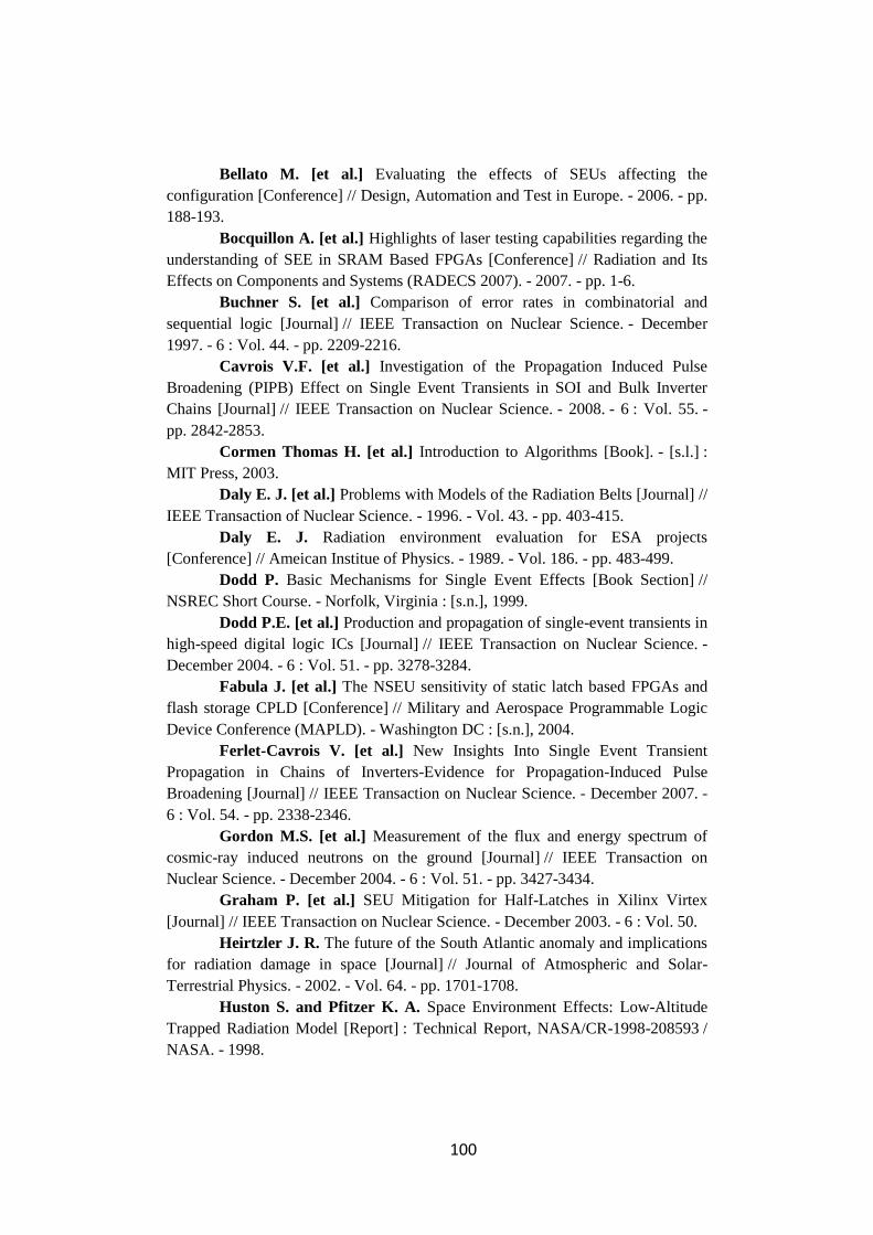
100
Bellato M. [et al.] Evaluating the effects of SEUs affecting the
configuration [Conference] // Design, Automation and Test in Europe. - 2006. - pp.
188-193.
Bocquillon A. [et al.] Highlights of laser testing capabilities regarding the
understanding of SEE in SRAM Based FPGAs [Conference] // Radiation and Its
Effects on Components and Systems (RADECS 2007). - 2007. - pp. 1-6.
Buchner S. [et al.] Comparison of error rates in combinatorial and
sequential logic [Journal] // IEEE Transaction on Nuclear Science. - December
1997. - 6 : Vol. 44. - pp. 2209-2216.
Cavrois V.F. [et al.] Investigation of the Propagation Induced Pulse
Broadening (PIPB) Effect on Single Event Transients in SOI and Bulk Inverter
Chains [Journal] // IEEE Transaction on Nuclear Science. - 2008. - 6 : Vol. 55. -
pp. 2842-2853.
Cormen Thomas H. [et al.] Introduction to Algorithms [Book]. - [s.l.] :
MIT Press, 2003.
Daly E. J. [et al.] Problems with Models of the Radiation Belts [Journal] //
IEEE Transaction of Nuclear Science. - 1996. - Vol. 43. - pp. 403-415.
Daly E. J. Radiation environment evaluation for ESA projects
[Conference] // Ameican Institue of Physics. - 1989. - Vol. 186. - pp. 483-499.
Dodd P. Basic Mechanisms for Single Event Effects [Book Section] //
NSREC Short Course. - Norfolk, Virginia : [s.n.], 1999.
Dodd P.E. [et al.] Production and propagation of single-event transients in
high-speed digital logic ICs [Journal] // IEEE Transaction on Nuclear Science. -
December 2004. - 6 : Vol. 51. - pp. 3278-3284.
Fabula J. [et al.] The NSEU sensitivity of static latch based FPGAs and
flash storage CPLD [Conference] // Military and Aerospace Programmable Logic
Device Conference (MAPLD). - Washington DC : [s.n.], 2004.
Ferlet-Cavrois V. [et al.] New Insights Into Single Event Transient
Propagation in Chains of Inverters-Evidence for Propagation-Induced Pulse
Broadening [Journal] // IEEE Transaction on Nuclear Science. - December 2007. -
6 : Vol. 54. - pp. 2338-2346.
Gordon M.S. [et al.] Measurement of the flux and energy spectrum of
cosmic-ray induced neutrons on the ground [Journal] // IEEE Transaction on
Nuclear Science. - December 2004. - 6 : Vol. 51. - pp. 3427-3434.
Graham P. [et al.] SEU Mitigation for Half-Latches in Xilinx Virtex
[Journal] // IEEE Transaction on Nuclear Science. - December 2003. - 6 : Vol. 50.
Heirtzler J. R. The future of the South Atlantic anomaly and implications
for radiation damage in space [Journal] // Journal of Atmospheric and Solar-
Terrestrial Physics. - 2002. - Vol. 64. - pp. 1701-1708.
Huston S. and Pfitzer K. A. Space Environment Effects: Low-Altitude
Trapped Radiation Model [Report] : Technical Report, NASA/CR-1998-208593 /
NASA. - 1998.
101
ITC’99 ITC’99 Benchmark homepage [Online]. -
http://www.cerc.utexas.edu/itc99-benchmarks/bench-html.
JEDEC Measurement and Reporting of Alpha Particles and Terrestrial
Cosmic Ray-Induced Soft Errors in Semiconductor Devices [Book] = JESD89A. -
[s.l.] : JEDEC SOLID STATE TECHNOLOGY ASSOCIATION, 2006.
Lesea A. [et al.] The rosetta experiment: atmospheric soft error rate testing
in differing technology FPGAs [Journal] // IEEE Transactions on Device and
Materials Reliability. - September 2005. - 3 : Vol. 5. - pp. 317-328.
Lima F. [et al.] A fault injection analysis of Virtex FPGA TMR design
methodology [Conference] // Radiation and Its Effects on Components and
Systems (RADECS). - 2001. - pp. 275-282 .
Lima Kastensmidt F.G. [et al.] Designing fault-tolerant techniques for
SRAM-based FPGAs [Journal] // IEEE Design & Test of Computers. -
November/December 2004. - 6 : Vol. 21. - pp. 552-562.
Lum G. Hardness Assurance for Space Systems [Book Section] / book
auth. Course IEEE Nuclear and Space Radiation Effects Conference Short. - 2004.
Miller F. [et al.] Laser Mapping of SRAM Sensitive Cells: A Way to
Obtain Input Parameters for DASIE Calculation Code [Journal] // IEEE
Transaction on Nuclear Science. - August 2006. - 4 : Vol. 53. - pp. 1863-1870.
Miller F. Experimental and theoretical study of the effects induced by a
pulsed laser in electronic devices and comparison with the single events induced by
natural radiation environment [Book]. - [s.l.] : Montpellier II Thesis, 2006.
Narasimham B. [et al.] Test Circuit for measuring pulse widths of single-
event transients causing soft errors [Conference] // IEEE International Conference
on Microelectronic Test Structure. - 2008. - pp. 142-146.
Normand E. and Baker T.J. Altitude and latitude variations in avionics
SEU and atmospheric neutron flux [Journal] // IEEE Transaction on Nuclear
Science. - 1993. - 6 : Vol. 51.
Pavan P. [et al.] Flash Memory Cells - An Overview [Journal] //
Proceedings of the IEEE. - August 1997. - 8 : Vol. 85. - pp. 1248-1271.
Peurrung A. J. Recent developments in neutron detection [Journal] //
Nuclear Instruments and Methods in Physics Research. - 2000. - 2-3 : Vol. 443. -
pp. 400-415 .
Platt S. P., Cassels B. and Torok Z. Development and application of a
neutron sensor for single event effects analysis [Journal] // Journal of Physics:
Conference Series. - 2005. - Vol. 15. - pp. 172-176.
Platt S.P. [et al.] Charge-collection and single-event upset measurements
at the ISIS neutron source [Conference] // European Conference on Radiation and
its Effects on Component and Systems (RADECS). - 2007.
Platt S.P. and Torok Z. Analysis of SEE-Inducing Charge Generation in
the Neutron Beam at The Svedberg Laboratory [Journal] // IEEE Transaction on
Nuclear Science. - 2007. - 4 : Vol. 54. - pp. 1163-1169.
102
Pontarelli Salvatore [et al.] Totally Fault Tolerant RNS based FIR Filters
[Conference] // IEEE International On-Line Testing Symposioum. - Rhodes,
Greece : [s.n.], 2008. - pp. 192-194.
Pratt Brian [et al.] Improving FPGA Design Robustness with Partial
TMR [Conference] // International Reliability Physics Symposium (IRPS). - 2006.
Quinn H. [et al.] A test methodology for determining space-readiness of
Xilinx SRAM-based FPGA designs [Conference] // IEEE AUTOTESTCON. -
2008. - pp. 252-258.
Quinn H.r [et al.] Reliability Concerns with Logical Constants in Xilinx
FPGA Designs [Conference] // Military and Aerospace Programmable Logic
Devices (MAPLD) Conference. - Annapolis : [s.n.], 2008.
Quinn Heather [et al.] Domain Crossing Errors: Limitations on Single
Device Triple-Modular Redundancy Circuits in Xilinx FPGA [Journal] // IEEE
Transaction on Nuclear Science. - December 2007. - 6 : Vol. 54. - pp. 2037-2043.
Quinn Heather [et al.] FPGAs, Radiation-Induced Multi-Bit Upsets in
SRAM-Based [Journal] // IEEE Transaction on Nuclear Science. - December
2005. - 6 : Vol. 52. - pp. 2455-2461.
Re M. [et al.] FPGA realization of RNS to binary signed conversion
architecture [Conference] // IEEE International Symposium on Circuits and
Systems. - 2001. - Vol. 4. - pp. 350-353.
Rezgui S. [et al.] A Few Guidelines for the SET Characterization of Non-
Volatile FPGAs: Lessons Learned [Conference] // Military and Aerospace
Programmable Logic Conference (MAPLD). - Annapolis, Maryland : [s.n.], 2008.
Rezgui S. [et al.] Comprehensive SEE characterization of 0.13µm flash-
based FPGAs by heavy ion beam test [Conference] // Radiation and Its Effects on
Components and Systems (RADECS). - 2007. - pp. 1-6.
Rezgui S. [et al.] Configuration and Routing Effects on the SET
Propagation in Flash-Based FPGAs [Journal] // IEEE Transaction on Nuclear
Science. - December 2008. - 6 : Vol. 55. - pp. 3328-3335.
Rezgui S. [et al.] New Methodologies for SET Characterization and
Mitigation in Flash-Based FPGAs [Journal] // IEEE Transaction on Nuclear
Science. - December 2007. - pp. 2512-2524.
Schwank J. R. [et al.] Effects of Total Dose Irradiation on Single-Event
Upset Hardness [Journal] // IEEE Transaction on Nuclear Science. - August 2006. -
4 : Vol. 53. - pp. 1772-1778.
Schwank J.R. [et al.] Radiation Effects in MOS Oxides [Journal] // IEEE
Transaction on Nuclear Science. - 2008. - 4 : Vol. 55. - pp. 1833-1853.
Sonza Reorda M., Sterpone L. and Violante M. Multiple errors
produced by single upsets in FPGA configuration memory: a possible solution
[Conference] // IEEE European Test Symposium. - 2005. - pp. 136-141.

103
Speers T. [et al.] 0.25UM Flash Memory Based FPGA For Space
Applications [Conference] // Military and Aerospace Programmable Logic
Conference (MAPLD). - Laurel, Maryland : [s.n.], 1999.
Sterpone L. and Violante M. A new Algorithm for the Analysis of the
MBUs Sensitiveness of TMR Architectures in SRAM-based FPGAs [Journal] //
IEEE Transaction on Nuclear Science. - 2008.
Sterpone L. and Violante M. A New Analytical Approach to Estimate the
Effects of SEUs in TMR Architecture Implemented Through SRAM-based FPGA
[Journal] // IEEE Transaction on Nuclear Science. - December 2005. - 6 : Vol. 52. -
pp. 2217-2223.
Sterpone L. and Violante M. A New Analytical Approach to Estimate the
Effects of SEUs in TMR Architectures Implemented Through SRAM-Based
FPGAs [Journal] // IEEE Transaction on Nuclear Science. - December 2005. - 6 :
Vol. 52. - pp. 2217-2223.
Sterpone L. and Violante M. A new reliability-oriented place and route
algorithm for SRAM-based FPGAs [Journal] // IEEE Transaction on Computer. -
June 2006. - 6 : Vol. 55. - pp. 732-744.
Sterpone L. and Violante M. A new reliability-oriented place and route
algorithm for SRAM-based FPGAs [Journal] // IEEE Transaction on Computer. -
June 2006. - 6 : Vol. 55. - pp. 732-744.
Swift G. VIRTEX-II Static SEU Characterization [Report]. - [s.l.] : Xilinx
SEE Consortium, 2004.
Swift G.M. [et al.] Static Upset Characteristics of the 90nm Virtex-4QV
FPGAs [Conference] // IEEE Radiation Effects Data Workshop. - 2008. - pp. 98-
105.
Szabó Nicholas S. and Tanaka Richard I. Residue arithmetic and its
applications to computer technology [Book]. - [s.l.] : McGraw-Hill, 1967.
Von Neumann J. Probabilistic Logics [Book Section] // Automata
Studies. - [s.l.] : Princeton University Press, 1956.
Watanabe N. Neutronics of pulsed spallation neutron sources [Journal] //
Reports on Progress in Physics. - 2003. - Vol. 66. - pp. 339-381.
Wirth G., Lima Kastensmidt F. and Ribeiro I. Single Event Transients
in Logic Circuits - Load and Propagation Induced Pulse Broadening [Journal] //
IEEE Transaction on Nuclear Science. - December 2008. - 6 : Vol. 55. - pp. 2928-
2935.
Xapsos M. Modeling the Space Radaition Environment [Book Section] //
IEEE Nuclear and Space Radiation Effects Conference Short Course. - 2006.
Xilinx Correcting Single-Event Upsets Through Virtex Partial
Configuration. - XAPP216.
Xilinx PicoBlaze 8-bit Embedded Microcontroller User Guide - UG129.
Xilinx Spartan-3 Generation Configuration User Guide. - UG332.
Xilinx Spartan-3 Generation FPGA User Guide. - UG331.
104
Xilinx TMRTool Sheet Xilinx [Online]. - 2006. -
http://www.xilinx.com/esp/mil_aero/collateral/tmrtool_sellsheet_wr.pdf.
Xilinx Triple Module Redundancy Design Techniques for Virtex FPGAs -
XAPP197.
Xilinx Xilinx TMRTool User Guide [Book]. - UG156.
Yui C.C. [et al.] SEU mitigation testing of Xilinx Virtex II FPGAs
[Conference] // IEEE Radiation Effects Data Workshop. - 2003. - pp. 92-97.

105
Acknowledgements
Many persons have contributed to my PhD research activities. I would like to
express my sincere gratitude to prof. Alessandro Paccagnella, who has been my
PhD supervisor. He provided me with many helpful suggestions,
important advice and constant encouragement during the course of this
work. I wish also to thank Dr. Simone Gerardin for his guidance and his
suggestions.
My warm thanks are due to all the people who I have been collaborating with. At
Politecnico di Torino: Dr. Luca Sterpone, Dr. Massimo Violante and Niccolò
Battezzati. At Università di Roma Tor Vergata, Dr. Salvatore Pontarelli. They all
have been fundamental in my formation and this work has been possible thanks to
them.
I would like to acknowledge my reviewer, prof. Fernanda Lima Kastensmidt, for
the careful review and the useful suggestions.
I especially thank all my friends and colleagues at Padova University: Marco
Silvestri, Alessio Griffoni, Marta Bagatin, Paolo Rech, Martino Fornasa, Alberto
Gasperin, Nicola Wrachien, Matteo Camponeschi, Alessio Vallese and Dr. Giorgio
Cellere. They provided me great support and encouragements, also outside the
academic field.
Many thanks to all the instrument scientists I have met in the various irradiation
facilities. Their help has been very important.
Very special thanks to my family; they have always been supporting and advising
me in all my choices. Concluding, I would like to thank the most important person,
Anna, who gave a new sense to my life.
Andrea Manuzzato
Padova, December 2009