Elenco delle pubblicazioni di Gianluca Traversi - UniBG · Elenco delle pubblicazioni di Gianluca...
21
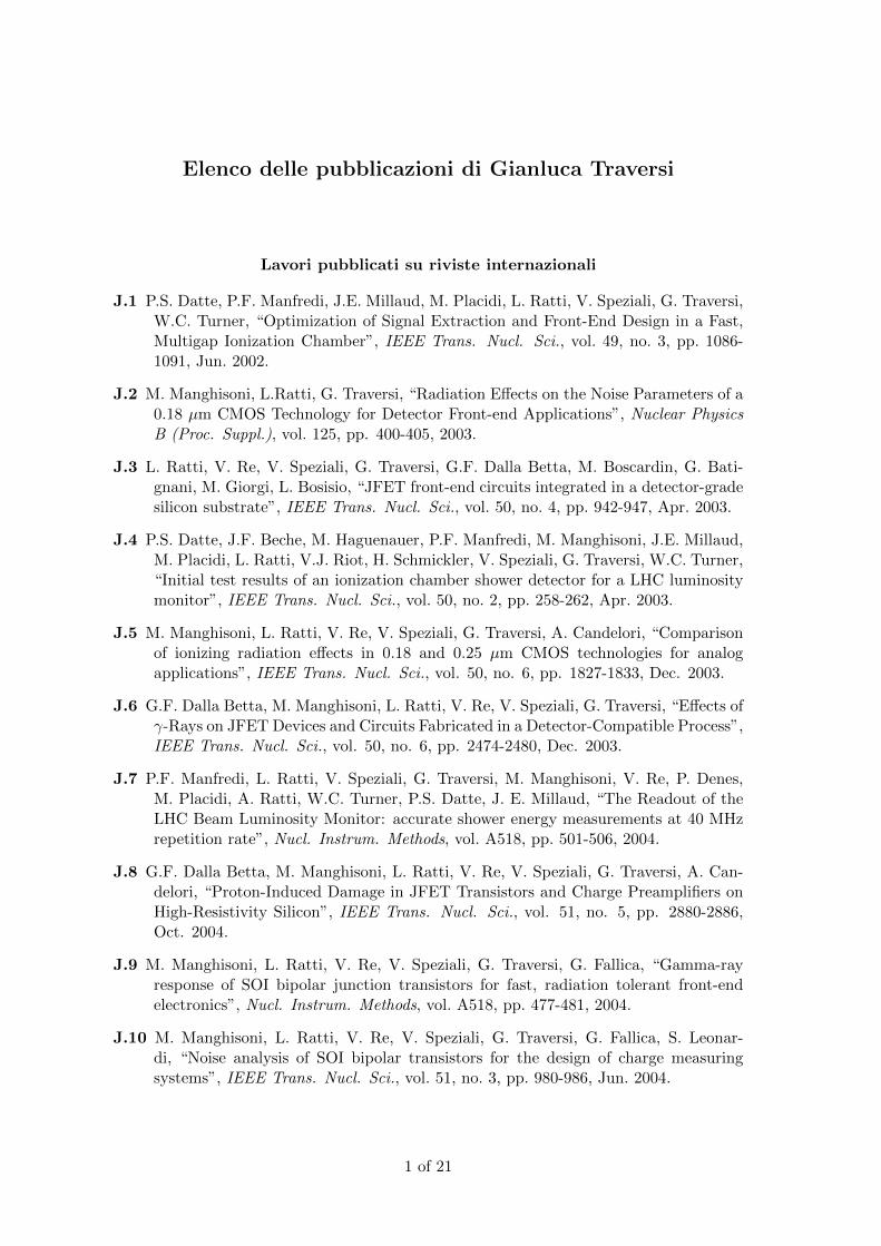
Elenco delle pubblicazioni di Gianluca Traversi Lavori pubblicati su riviste internazionali J.1 P.S. Datte, P.F. Manfredi, J.E. Millaud, M. Placidi, L. Ratti, V. Speziali, G. Traversi, W.C. Turner, “Optimization of Signal Extraction and Front-End Design in a Fast, Multigap Ionization Chamber”, IEEE Trans. Nucl. Sci., vol. 49, no. 3, pp. 1086- 1091, Jun. 2002. J.2 M. Manghisoni, L.Ratti, G. Traversi, “Radiation Effects on the Noise Parameters of a 0.18 μm CMOS Technology for Detector Front-end Applications”, Nuclear Physics B (Proc. Suppl.), vol. 125, pp. 400-405, 2003. J.3 L. Ratti, V. Re, V. Speziali, G. Traversi, G.F. Dalla Betta, M. Boscardin, G. Bati- gnani, M. Giorgi, L. Bosisio, “JFET front-end circuits integrated in a detector-grade silicon substrate”, IEEE Trans. Nucl. Sci., vol. 50, no. 4, pp. 942-947, Apr. 2003. J.4 P.S. Datte, J.F. Beche, M. Haguenauer, P.F. Manfredi, M. Manghisoni, J.E. Millaud, M. Placidi, L. Ratti, V.J. Riot, H. Schmickler, V. Speziali, G. Traversi, W.C. Turner, “Initial test results of an ionization chamber shower detector for a LHC luminosity monitor”, IEEE Trans. Nucl. Sci., vol. 50, no. 2, pp. 258-262, Apr. 2003. J.5 M. Manghisoni, L. Ratti, V. Re, V. Speziali, G. Traversi, A. Candelori, “Comparison of ionizing radiation effects in 0.18 and 0.25 μm CMOS technologies for analog applications”, IEEE Trans. Nucl. Sci., vol. 50, no. 6, pp. 1827-1833, Dec. 2003. J.6 G.F. Dalla Betta, M. Manghisoni, L. Ratti, V. Re, V. Speziali, G. Traversi, “Effects of γ -Rays on JFET Devices and Circuits Fabricated in a Detector-Compatible Process”, IEEE Trans. Nucl. Sci., vol. 50, no. 6, pp. 2474-2480, Dec. 2003. J.7 P.F. Manfredi, L. Ratti, V. Speziali, G. Traversi, M. Manghisoni, V. Re, P. Denes, M. Placidi, A. Ratti, W.C. Turner, P.S. Datte, J. E. Millaud, “The Readout of the LHC Beam Luminosity Monitor: accurate shower energy measurements at 40 MHz repetition rate”, Nucl. Instrum. Methods, vol. A518, pp. 501-506, 2004. J.8 G.F. Dalla Betta, M. Manghisoni, L. Ratti, V. Re, V. Speziali, G. Traversi, A. Can- delori, “Proton-Induced Damage in JFET Transistors and Charge Preamplifiers on High-Resistivity Silicon”, IEEE Trans. Nucl. Sci., vol. 51, no. 5, pp. 2880-2886, Oct. 2004. J.9 M. Manghisoni, L. Ratti, V. Re, V. Speziali, G. Traversi, G. Fallica, “Gamma-ray response of SOI bipolar junction transistors for fast, radiation tolerant front-end electronics”, Nucl. Instrum. Methods, vol. A518, pp. 477-481, 2004. J.10 M. Manghisoni, L. Ratti, V. Re, V. Speziali, G. Traversi, G. Fallica, S. Leonar- di, “Noise analysis of SOI bipolar transistors for the design of charge measuring systems”, IEEE Trans. Nucl. Sci., vol. 51, no. 3, pp. 980-986, Jun. 2004. 1 of 21
Transcript of Elenco delle pubblicazioni di Gianluca Traversi - UniBG · Elenco delle pubblicazioni di Gianluca...
Elenco delle pubblicazioni di Gianluca Traversi
Lavori pubblicati su riviste internazionali
J.1 P.S. Datte, P.F. Manfredi, J.E. Millaud, M. Placidi, L. Ratti, V. Speziali, G. Traversi,W.C. Turner, “Optimization of Signal Extraction and Front-End Design in a Fast,Multigap Ionization Chamber”, IEEE Trans. Nucl. Sci., vol. 49, no. 3, pp. 1086-1091, Jun. 2002.
J.2 M. Manghisoni, L.Ratti, G. Traversi, “Radiation Effects on the Noise Parameters of a0.18 µm CMOS Technology for Detector Front-end Applications”, Nuclear PhysicsB (Proc. Suppl.), vol. 125, pp. 400-405, 2003.
J.3 L. Ratti, V. Re, V. Speziali, G. Traversi, G.F. Dalla Betta, M. Boscardin, G. Bati-gnani, M. Giorgi, L. Bosisio, “JFET front-end circuits integrated in a detector-gradesilicon substrate”, IEEE Trans. Nucl. Sci., vol. 50, no. 4, pp. 942-947, Apr. 2003.
J.4 P.S. Datte, J.F. Beche, M. Haguenauer, P.F. Manfredi, M. Manghisoni, J.E. Millaud,M. Placidi, L. Ratti, V.J. Riot, H. Schmickler, V. Speziali, G. Traversi, W.C. Turner,“Initial test results of an ionization chamber shower detector for a LHC luminositymonitor”, IEEE Trans. Nucl. Sci., vol. 50, no. 2, pp. 258-262, Apr. 2003.
J.5 M. Manghisoni, L. Ratti, V. Re, V. Speziali, G. Traversi, A. Candelori, “Comparisonof ionizing radiation effects in 0.18 and 0.25 µm CMOS technologies for analogapplications”, IEEE Trans. Nucl. Sci., vol. 50, no. 6, pp. 1827-1833, Dec. 2003.
J.6 G.F. Dalla Betta, M. Manghisoni, L. Ratti, V. Re, V. Speziali, G. Traversi, “Effects ofγ-Rays on JFET Devices and Circuits Fabricated in a Detector-Compatible Process”,IEEE Trans. Nucl. Sci., vol. 50, no. 6, pp. 2474-2480, Dec. 2003.
J.7 P.F. Manfredi, L. Ratti, V. Speziali, G. Traversi, M. Manghisoni, V. Re, P. Denes,M. Placidi, A. Ratti, W.C. Turner, P.S. Datte, J. E. Millaud, “The Readout of theLHC Beam Luminosity Monitor: accurate shower energy measurements at 40 MHzrepetition rate”, Nucl. Instrum. Methods, vol. A518, pp. 501-506, 2004.
J.8 G.F. Dalla Betta, M. Manghisoni, L. Ratti, V. Re, V. Speziali, G. Traversi, A. Can-delori, “Proton-Induced Damage in JFET Transistors and Charge Preamplifiers onHigh-Resistivity Silicon”, IEEE Trans. Nucl. Sci., vol. 51, no. 5, pp. 2880-2886,Oct. 2004.
J.9 M. Manghisoni, L. Ratti, V. Re, V. Speziali, G. Traversi, G. Fallica, “Gamma-rayresponse of SOI bipolar junction transistors for fast, radiation tolerant front-endelectronics”, Nucl. Instrum. Methods, vol. A518, pp. 477-481, 2004.
J.10 M. Manghisoni, L. Ratti, V. Re, V. Speziali, G. Traversi, G. Fallica, S. Leonar-di, “Noise analysis of SOI bipolar transistors for the design of charge measuringsystems”, IEEE Trans. Nucl. Sci., vol. 51, no. 3, pp. 980-986, Jun. 2004.
1 of 21

J.11 G. Traversi et al., “Recent results from the development of silicon detectors withintegrated electronics”, Nucl. Instrum. Methods, vol. A518, pp. 354-356, 2004.
J.12 M. Manghisoni, E. Oberti, L. Ratti, V. Re, V. Speziali, G. Traversi, G. Fallica, R.Modica, “Response of SOI bipolar transistors exposed to γ-rays under different doserate and bias conditions”, IEEE Trans. Nucl. Sci., vol. 52, no. 4, pp. 1040-1047,Aug. 2005.
J.13 V. Re, M. Manghisoni, L. Ratti, V. Speziali, G. Traversi, “Survey of noise performan-ces and scaling effects in deep submicron CMOS devices from different foundries”,IEEE Trans. Nucl. Sci., vol. 52, no. 6, part. 2, pp. 2733-2740, Dec. 2005.
J.14 V. Re, M. Manghisoni, L. Ratti, V. Speziali, G. Traversi, “Total Ionizing Dose Effectson the Noise Performances of a 0.13 µm CMOS Technology”, IEEE Trans. Nucl.Sci., vol. 53, no. 3, pp. 1599-1606, Jun. 2006.
J.15 G. Rizzo, S. Bettarini, G. Calderini, R. Cenci, F. Forti, M.A. Giorgi, F. Morsani, L.Ratti, V. Speziali, M. Manghisoni, V. Re, G. Traversi, L. Bosisio, “A novel monolithicactive pixel detector in 0.13 µm triple well CMOS technology with pixel level analogprocessing”, Nucl. Instrum. Methods, vol. A565, pp. 195-201, 2006.
J.16 M. Manghisoni, L. Ratti, V. Re, V. Speziali, G. Traversi, “Noise performance of0.13 µm CMOS technologies for detector front-end applications”, IEEE Trans. Nucl.Sci., vol. 53, no. 4, pp. 2456-2462, Aug. 2006.
J.17 L. Ratti, M. Manghisoni, V. Re, V. Speziali, G. Traversi, S. Bettarini, G. Calderini,R. Cenci, M. Giorgi, F. Forti, F. Morsani, G. Rizzo, “Monolithic pixel detectors ina 0.13 µm CMOS technology with sensor level continuous time charge amplificationand shaping”, Nucl. Instrum. Methods, vol. A568, pp. 159-166, 2006.
J.18 V. Re, M. Manghisoni, L. Ratti, V. Speziali, G. Traversi, “Design criteria forlow-noise front-end electronics in the 0.13 µm CMOS generation”, Nucl. Instrum.Methods, vol. A568, pp. 343-349, 2006.
J.19 G. Traversi et al., “A new approach to the design of monolithic active pixel detectorsin 0.13 µm triple well CMOS technology”, Nucl. Instrum. Methods, vol. A569,pp. 61-64, 2006.
J.20 M. Manghisoni, L. Ratti, V. Re, V. Speziali, G. Traversi, “130 and 90 nm CMOStechnologies for detector front-end applications”, Nucl. Instrum. Methods, vol. A572,pp. 368-370, 2007.
J.21 G. Traversi M. Manghisoni, L. Ratti, V. Re, V. Speziali, “Pixel-level continuous-time analog signal processing for 130 nm CMOS MAPS”, Nucl. Instrum. Methods,vol. A572, pp. 396-398, 2007.
J.22 V. Re, M. Manghisoni, L. Ratti, G. Traversi, V. Speziali, “Impact of Lateral IsolationOxides on Radiation-Induced Noise Degradation in CMOS Technologies in the 100nm Regime”, IEEE Trans. Nucl. Sci., vol. 54, no. 6 part. 1, pp. 2218-2226, Dec.2007.
2 of 21
J.23 G. Traversi et al., “Development of deep N-well monolithic active pixel sensors in a0.13 µm CMOS technology”, Nucl. Instrum. Methods, vol. A572, pp. 277-280, 2007.
J.24 M. Manghisoni, L. Ratti, V. Re, V. Speziali, G. Traversi, “Resolution Limits in130 nm and 90 nm CMOS Technologies for Analog Front-End Applications”, IEEETrans. Nucl. Sci., vol. 54, no. 3, pp. 531-537, Jun. 2007.
J.25 G. Traversi, M. Manghisoni, L. Ratti, V. Re, V. Speziali, “CMOS MAPS with pixellevel sparsification and time stamping capabilities for applications at the ILC”, Nucl.Instrum. Methods, vol. A581, pp. 291-294, 2007.
J.26 G Traversi et al., “Recent developments in 130nm CMOS monolithic active pixeldetectors”, Nuclear Physics B, vol. 172, pp. 20-24, Oct. 2007.
J.27 G. Traversi et al., “Development of a triple well CMOS MAPS device with in-pixelsignal processing and sparsified readout capabilities”, Nucl. Instrum. Methods,vol. A581, pp. 303-305, 2007.
J.28 V. Re, L. Gaioni, M. Manghisoni, L. Ratti, V. Speziali, G. Traversi, “CMOS Tech-nologies in the 100 nm range for rad-hard front-end electronics in future colliderexperiments”, Nucl. Instrum. Methods, vol. A596 (1), pp. 107-112, Oct. 2008.
J.29 G. Traversi et al., “Proposal of a sparsification circuit for mixed-mode MAPS de-tectors”, Nucl. Instrum. Methods, vol. A596 (1), pp. 93-95, Oct. 2008.
J.30 L. Ratti, L. Gaioni, M. Manghisoni, G. Traversi, D. Pantano, “Investigating Degra-dation Mechanisms in 130 nm and 90 nm Commercial CMOS Technologies Under Ex-treme Radiation Conditions”, IEEE Trans. Nucl. Sci., vol. 55, no. 4, pp. 1992-2000,Aug. 2008.
J.31 V. Re, L. Gaioni, M. Manghisoni, L. Ratti, V. Speziali, G. Traversi, R. Yarema, “Noi-se behavior of a 180nm CMOS SOI Technology for Detector Front-end Electronics”,IEEE Trans. Nucl. Sci., vol. 55, no. 4, pp. 2408-2413, Aug. 2008.
J.32 G. Traversi et al., “Monolithic Active Pixel Sensors for the Vertex Detector at theInternational Linear Collider”, Il Nuovo Cimento B, Vol. 123, Issue 06-07, pp. 994-996, Nov. 2008.
J.33 V. Re, L. Gaioni, M. Manghisoni, L. Ratti, G. Traversi, “Comprehensive Study ofTotal Ionizing Dose Damage Mechanisms and Their Effects on Noise Sources in a90nm CMOS Technology”, IEEE Trans. Nucl. Sci., vol. 55, no. 6, pp. 3272-3279,Dec. 2008.
J.34 G. Traversi et al., “On-chip fast data sparsification for a monolithic 4096-pixeldevice”, IEEE Trans. Nucl. Sci., vol. 56, no. 3, pp. 1159-1162, June 2009.
J.35 G. Traversi et al., “A 4096-pixel MAPS device with on-chip data sparsification”,Nucl. Instrum. Methods, vol. A604 (1-2), pp. 408-411, June 2009.
3 of 21

J.36 G. Traversi, A. Bulgheroni, M. Caccia, M Jastrzab, M. Manghisoni, E. Pozzati, L.Ratti, V. Re, “Design and Performance of a DNW CMOS Active Pixel Sensor forthe ILC Vertex Detector”, IEEE Trans. Nucl. Sci., vol. 56 (5), pp. 3002-3009, Oct.2009.
J.37 L. Ratti, C. Andreoli, L. Gaioni, M. Manghisoni, Enrico Pozzati, V. Re, G. Traversi,“TID effects in deep N-well CMOS monolithic active pixel sensors”, IEEE Trans.Nucl. Sci., vol. 56, no. 4, pp. 2124-2131, Aug. 2009.
J.38 L. Ratti, M. Manghisoni, V. Re, G. Traversi, “Design of Time Invariant AnalogFront-End Circuits for Deep N-Well CMOS MAPS”, IEEE Trans. Nucl. Sci., vol. 56,no. 4, pp. 2360-2373, Aug. 2009.
J.39 G. Traversi, A. Bulgheroni, M. Caccia, M Jastrzab, M. Manghisoni, E. Pozzati,L. Ratti, V. Re, “First Generation of Deep N-Well CMOS MAPS with in-pixelSparsification for the ILC Vertex Detector”, Nucl. Instrum. Methods, vol. A604(1-2), pp. 390-392, June 2009.
J.40 L. Ratti, M. Manghisoni, V. Re, G. Traversi, “Design Optimization of Charge Pre-amplifiers with CMOS Processes in the 100 nm Gate Length Regime”, IEEE Trans.Nucl. Sci., vol. 56, no. 1, pp. 235-242, Feb. 2009.
J.41 G. Traversi et al., “The high rate data acquisition system for the SLIM5 beam test”,Nucl. Instrum. Methods, vol. A617 (1-3), pp.321-323, May. 2010.
J.42 G. Traversi et al., “Beam-test results of 4k pixel CMOS MAPS and high resistivitystriplet detectors equipped with digital sparsified readout in the Slim5 low masssilicon demonstrator”, Nucl. Instrum. Methods, vol. A617 (1-3), pp. 596-600, May.2010.
J.43 G. Traversi et al., “SLIM5 beam test results for thin striplet detector and fast readoutbeam telescope”, Nucl. Instrum. Methods, vol. A617 (1-3), pp. 601-604, May. 2010.
J.44 G. Traversi et al., “The superB silicon vertex tracker”, Nucl. Instrum. Methods,vol. A617 (1-3), pp. 585-587, May. 2010.
J.45 L. Ratti, V. Re, M. Manghisoni, L. Gaioni, G. Traversi, “Vertically integrated deepN-well CMOS MAPS with sparsification and time stamping capabilities for thincharged particle trackers”, Nucl. Instrum. Methods, vol. A624 (2), pp. 379-386,Dec. 2010.
J.46 G. Traversi et al., “Deep n-well MAPS in a 130 nm CMOS technology: Beam testresults”, Nucl. Instrum. Methods, vol. A623 (1), pp. 195-197, Nov. 2010.
J.47 G. Traversi et al., “The SLIM5 low mass silicon tracker demonstrator”, Nucl. In-strum. Methods, vol. A623 (3), pp. 942-953, Nov. 2010.
J.48 M. Manghisoni, V. Re, L. Gaioni, L. Ratti, G. Traversi, “Introducing 65nm CMOStechnology in low-noise read-out of semiconductor detectors”, Nucl. Instrum. Me-thods, vol. A624 (2), pp. 373-378, Dec. 2010.
4 of 21
J.49 L. Gaioni, M. Manghisoni, L. Ratti, V. Re, G. Traversi,“A 3D deep n-well CMOSMAPS for the ILC vertex detector”, Nucl. Instrum. Methods, vol. A617 (1-3), pp.324-326, May. 2010.
J.50 V. Re, M. Manghisoni, L. Gaioni, L. Ratti, G. Traversi, “Forecasting noise andradiation hardness of CMOS front-end electronics beyond the 100nm frontier”, Nucl.Instrum. Methods, vol. A617 (1-3), pp. 358-361, May. 2010.
J.51 V. Re, L. Gaioni, M. Manghisoni, L. Ratti, G. Traversi, “Mechanisms of NoiseDegradation in Low Power 65 nm CMOS Transistors Exposed to Ionizing Radiation”,IEEE Trans. Nucl. Sci., vol. 57, no. 6, pp. 3071-3077, Dec 2010.
J.52 L. Ratti, M. Manghisoni, V. Re, G. Traversi, S. Zucca, S. Bettarini, F. Morsani, G.Rizzo, “Front-end performance and charge collection properties of heavily irradiatedDNW MAPS”, IEEE Trans. Nucl. Sci., vol. 57, no. 4, pp. 1781-1789, Aug. 2010.
J.53 A. Manazza, L. Gaioni, L. Ratti, G. Traversi, S. Zucca, V. Re,“Analog front-end forpixel sensors in a 3D CMOS technology for the SuperB Layer0”, Il Nuovo CimentoC, vol. 34 (6), p. 57-59, 2011, ISSN: 1826-9885, doi: 10.1393/ncc/i2011-11026-5.
J.54 L. Ratti, L. Gaioni, M. Manghisoni, V. Re, G. Traversi “TID-Induced Degradationin Static and Noise Behavior of Sub-100 nm Multifinger Bulk NMOSFETs”, IEEETrans. Nucl. Sci., vol. 58, no. 3, pp. 776-784, June. 2011.
J.55 L. Gaioni, M. Manghisoni, L. Ratti, V. Re, G. Traversi “Front-end electronics ina 65 nm CMOS process for high density readout of pixel sensors”, Nucl. Instrum.Methods, vol. A650, pp. 163-168, Sept. 2011.
J.56 G. Traversi, L. Gaioni, M. Manghisoni, L. Ratti, V. Re, “2D and 3D CMOS MAPSwith high performance pixel-level signal processing”, Nucl. Instrum. Methods,vol. A628 (1), pp. 212-215, Feb. 2011.
J.57 G. Traversi et al., “Beam Test Results of Different Configurations of Deep N-wellMAPS Matrices Featuring in Pixel Full Signal Processing”, Nucl. Instrum. Methods,vol. A628 (1), pp. 234-237, Feb. 2011.
J.58 L. Ratti, L. Gaioni, M. Manghisoni, V. Re, G. Traversi “Vertically integrated pi-xel sensors for charged particle tracking and biomedical imaging”, Nucl. Instrum.Methods, vol. A652 (1), pp. 630-633, Oct. 2011.
J.59 G. Traversi et al., “Thin Pixel Development for the SuperB Silicon Vertex Tracker”,Nuclear Physics B, vol. 215 (1), pp. 284-286, June 2011.
J.60 G. Traversi, L. Gaioni, M. Manghisoni, L. Ratti, V. Re, “A 3D Vertically IntegratedDeep N-Well CMOS MAPS for the SuperB Layer0”, Journal of Instrumentation,vol. 6, C01010, Jan. 2011.
J.61 G. Traversi et al., “The SUPERB silicon vertex tracker”, Nucl. Instrum. Methods,vol. A636, pp. 168-172, April 2011.
5 of 21

J.62 G. Traversi et al., “Thin pixel development for the SuperB silicon vertex tracker”,Nucl. Instrum. Methods, vol. A650, pp. 169-173, Sept. 2011.
J.63 G. Traversi, “Charge signal processors in a 130 nm CMOS technology for the sparsereadout of small pitch monolithic and hybrid pixel sensors”, IEEE Trans. Nucl.Sci., vol. 58, no. 5, pp. 2391-2400, Oct. 2011.
J.64 G. Traversi, L. Gaioni, A. Manazza, M. Manghisoni, L. Ratti, V. Re, S. Zucca,“Recent progress in the development of 3D deep n-well CMOS MAPS”, Journal ofInstrumentation, vol. 7, C02006, Feb. 2012.
J.65 S. Zucca, L. Ratti, G. Traversi, S. Bettarini, F. Morsani, G. Rizzo, L. Bosisio, I.Rashevskaya, V. Cindro, “Characterization of bulk damage in CMOS MAPS withdeep N-well collecting electrode”, IEEE Trans. Nucl. Sci., vol. 59, no. 4, pp. 900-908,Aug. 2012.
J.66 G. Traversi, L. Gaioni, A. Manazza, M. Manghisoni, L. Ratti, V. Re, S. Zucca,“Recent progress in the development of 3D deep n-well CMOS MAPS”, Journal ofInstrumentation, vol. 7, C02006, Feb. 2012.
J.67 L. Gaioni, M. Manghisoni, L. Ratti, V. Re, G. Traversi, “A 65-nm CMOS PrototypeChip With Monolithic Pixel Sensors and Fast Front-End Electronics”, IEEE Trans.Nucl. Sci., vol. 59, no. 6(2), pp. 3304-3311, Dec. 2012.
J.68 L. Ratti, L. Gaioni, G. Traversi, S. Zucca, S. Bettarini, F. Morsani, G. Rizzo, L.Bosisio, I. Rashevskaya, “Modeling charge loss in CMOS MAPS exposed to non-ionizing radiation”, IEEE Trans. Nucl. Sci., vol. 60, no. 4, pp. 2574-2582, 2013.
J.69 V. Re, L. Gaioni, A. Manazza, M. Manghisoni, L. Ratti, G. Traversi, “RadiationTolerance of Devices and Circuits in a 3D Technology Based on the Vertical Inte-gration of Two 130-nm CMOS Layers”, IEEE Trans. Nucl. Sci., vol. 60, no. 6,pp. 4526-4532, 2013.
J.70 S. Zucca, L. Gaioni, L. Ratti, V. Re, G. Traversi, S. Bettarini, F. Forti, F. Morsani,G. Rizzo, L. Bosisio, I. Rashevskaya, “Monolithic pixel sensors for fast silicon vertextrackers in a quadruple well CMOS technology”, IEEE Trans. Nucl. Sci., vol. 60,no. 3, pp. 2343-2351, 2013.
J.71 G. Traversi, L. Gaioni, A. Manazza, M. Manghisoni, L. Ratti, V. Re, “The first fullyfunctional 3D CMOS chip with Deep N-well active pixel sensors for the ILC vertexdetector”, Nucl. Instrum. Meth., vol. 723, pp. 543-546, 2013.
J.72 L. Gaioni, M. Manghisoni, L. Ratti, V. Re, G. Traversi, “The design of fast analogchannels for the readout of strip detectors in the inner layers of the SuperB SVT”,
6 of 21

Nucl. Instrum. Meth., vol. 718, pp. 205-207, 2013.
J.73 M. Manghisoni et al., “The front-end chip of the SuperB SVT detector”, Nucl. In-strum. Meth., vol. 718, pp. 180-183, 2013.
J.74 M. Manghisoni et al., “Recent developments on CMOS MAPS for the SuperB Sili-con Vertex Tracker”, Nucl. Instrum. Meth., vol. 718, pp. 283-287, 2013.
J.75 M. Manghisoni et al., “Beam test results for the SuperB-SVT thin striplet detector”,Nucl. Instrum. Meth., vol. 718, pp. 314-317, 2013.
J.76 M. Manghisoni et al., “Latest results of the R&D on CMOS MAPS for the Layer0of the SuperB SVT”, Nucl. Instrum. Meth., vol. 732, pp. 484-487, 2013.
J.77 M. Manghisoni et al., “Advances in the development of pixel detector for the SuperBSilicon Vertex Tracker”, Nucl. Instrum. Meth., vol. 731, pp. 25-30, 2013.
J.78 L. Ratti, L. Gaioni, A. Manazza, M. Manghisoni, V. Re, G. Traversi, “First resultsfrom the characterization of a three-dimensional deep N-well MAPS prototype forvertexing applications”, Nucl. Instrum. Meth., vol. 699, pp. 41-46, 2013.
J.79 G. Traversi, L. Gaioni, A. Manazza, M. Manghisoni, L. Ratti, V. Re, S. Zucca, S.Bettarini, G. Rizzo, F. Morsani, L. Bosisio, I. Rashevskaya, V. Cindro, “Review ofradiation damage studies on DNW CMOS MAPS”, Nucl. Instrum. Meth., vol. 730,pp. 155-158, 2013.
J.80 M. Manghisoni, L. Gaioni, L. Ratti, V. Re, G. Traversi, “Assessment of a Low-Power65 nm CMOS Technology for Analog Front-End Design”, IEEE Trans. Nucl. Sci.,vol. 61, no. 1, pp. 553-560, 2014.
J.81 S. Zucca, L. Ratti, G. Traversi, F. Morsani, A. Gabrielli, F. Giorgi, “A quadruplewell CMOS MAPS prototype for the Layer0 of the SuperB SVT”, Nucl. Instrum.Meth., vol. 718, pp. 380-382, 2013.
J.82 A. Manazza, L. Gaioni, M. Manghisoni, V. Re, G. Traversi, S. Bettarini, F. Forti,F. Morsani, G. Rizo, “CMOS MAPS in a Homogeneous 3D Process for ChargedParticle Tracking”, IEEE Trans. Nucl. Sci., vol. 61, no. 1, pp. 700-707, 2014.
7 of 21
J.83 S. Zucca, M. Manghisoni, L. Ratti, V. Re, G. Traversi, S. Bettarini, F. Forti, F.Morsani, G. Rizzo, “Effects of substrate thinning on the properties of quadruplewell CMOS MAPS”, IEEE Trans. Nucl. Sci., vol. 61, pp. 1039-1046, 2014.
J.84 L. Ratti, G. Traversi, S. Zucca, S. Bettarini, F. Morsani, G. Rizzo, L. Bosisio, I.Rashevskaya, “Quadruple Well CMOS MAPS with time-invariant processor expo-sed to ionizing radiation and neutrons”, IEEE Trans. Nucl. Sci., vol. 61, no. 4,pp. 1763-1771, Aug. 2014.
J.85 L. Ratti L. Gaioni, A. Manazza, M. Manghisoni, V. Re, G. Traversi, “Advantages ofa vertical integration process in the design of DNW MAPS”, Nucl. Instrum. Meth.,vol. 784, pp. 255-259, 2015.
J.86 G. Traversi, F. De Canio, L. Gaioni, M. Manghisoni, L. Ratti, V. Re, “Design ofbandgap reference circuits in a 65 nm CMOS technology for HL-LHC applications”,Journal of Instrumentation, vol. 10, pp. 1-9, 2015.
J.87 G. Traversi, S. Bonacini, F. De Canio, L. Gaioni, K. Kloukinas, M. Manghisoni,L. Ratti, V. Re, “Design of low-power, low-voltage, differential I/O links for HighEnergy Physics applications”, Journal of Instrumentation, vol. 10, pp. 1-8, 2015.
J.88 L. Gaioni, F. De Canio, M. Manghisoni, L. Ratti, V. Re, G. Traversi, A. Marchioro,K. Kloukinas, “Low-power clock distribution circuits for the Macro Pixel ASIC”,Journal of Instrumentation, vol. 10, pp. 1-10, 2015.
J.89 G. Traversi et al., “PixFEL: developing a fine pitch, fast 2D X-ray imager for thenext generation X-FELs”, Nucl. Instrum. Meth., vol. 796.
J.90 G. Traversi et al., “The PixFEL project: development of advanced X-ray pixel de-tectors for application at future FEL facilities”, Journal of Instrumentation, vol. 10,2015.
J.91 G. Traversi et al., “Impact of low-dose electron irradiation on n+p silicon strip sen-sors”, Nucl. Instrum. Meth., vol. 803, pp. 100-112, Dec. 2015.
J.92 G. Blanchot, F. De Canio, T. Gadek, A. Honma, M. Kovacs, P. Rose, G. Tra-versi, “Transmission lines implementation on HDI flex circuits for the CMS trac-ker upgrade”, Journal of Instrumentation, vol. 11, Jan. 2016, doi: 10.1088/1748-0221/11/01/C01081
8 of 21

J.93 T. Vergine, M. De Matteis, S. Michelis, G. Traversi, F. De Canio, A. Baschirotto, “A65 nm Rad-Hard Bandgap Voltage Reference for LHC Environment”, IEEE Trans.Nucl. Sci., vol. 63, no. 3, pp. 1762-1767, June 2016.
J.94 G. Traversi et al., “A 2D imager for X-ray FELs with a 65 nm CMOS readout basedon per-pixel signal compression and 10 bit A/D conversion”, Nucl. Instrum. Meth.,vol. 831, pp. 301-308, Sept. 2016.
J.95 G. Traversi et al., “Design and TCAD simulation of planar p-on-n active-edge pixelsensors for the next generation of FELs”, Nucl. Instrum. Meth., vol. 824, pp. 384-385, 2016.
J.96 G. Traversi et al., “In-pixel conversion with a 10 bit SAR ADC for next generationX-ray FELs”, Nucl. Instrum. Meth., vol. 024, pp. 313-315, 2016.
J.97 G. Traversi, F. De Canio, L. Gaioni, M. Manghisoni, S. Mattiazzo, L. Ratti, V.Re, E. Riceputi, “Characterization of bandgap reference circuits designed for highenergy physics applications”, Nucl. Instrum. Meth., vol. 824, pp. 371-373, 2016.
J.98 G. Traversi et al., “ The PixFEL project: Progress towards a fine pitch X-ray ima-ging camera for next generation FEL facilities”, Nucl. Instrum. Meth., vol. 824,pp. 131-134, 2016.
J.99 L. Gaioni, F. De Canio, M. Manghisoni, L. Ratti, V. Re, G. Traversi, “Design andtest of clock distribution circuits for the Macro Pixel ASIC”, Nucl. Instrum. Meth.,vol. 824, pp. 287-289, 2016.
J.100 L. Gaioni, F. De Canio, M. Manghisoni, L. Ratti, V. Re, G. Traversi, “65 nmCMOS analog front-end for pixel detectors at the HL-LHC”, Journal of Instrumen-tation, vol. 11, 2016.
9 of 21
Lavori pubblicati su atti di congressi internazionali
P.1 P.S. Datte, P.F. Manfredi, J.E. Millaud, W.C. Turner, M. Placidi, L. Ratti, V. Spe-ziali, G. Traversi, “Electrical Design Considerations for a 40 MHz Gas IonizationChamber”, Proceedings of the 2001 Particle Accelerator Conference, vol. 2, pp.1327-1329, 18-22 June 2001, Chicago, Illinois (USA).
P.2 P.S. Datte, P.F. Manfredi, J.E. Millaud, M. Placidi, L. Ratti, V. Speziali, G. Tra-versi, W.C. Turner, “Optimization of signal extraction and front-end design in afast, multigap ionization chamber”, Nuclear Science Symposium Conference Re-cords, 2001, IEEE, San Diego, CA, USA, vol. 2, pp. 655-660, doi: 10.1109/NSS-MIC.2001.1009646.
P.3 G. Traversi et al., “Fabrication of Microstrip Detectors and Integrated Electronicson High Resistivity Silicon”, Proceedings of the 7th International Conference onAdvanced Technology and Particle Physics, pp. 241-245, 15-19 Oct. 2001, VillaOlmo, Como (Italia). Copyright 2002 World Scientific Publishing Co., ISBN 981-238-180-5.
P.4 G.F. Dalla Betta, M. Manghisoni, L. Ratti, V. Re, V. Speziali, G. Traversi, “Ionizingradiation effects on JFET devices and circuits fabricated in a detector-compatibleprocess”, Proceedings European Conference on Radiation and its Effects on Compo-nents and Systems (RADECS 2002), pp. 21-24, 19-20 Sep. 2002, Padova (Italia).
P.5 Manghisoni, Ratti, G. Traversi, “X-ray effects on the noise performances of 0.18and 0.25 µm CMOS processes for front-end applications”, Proceedings of the 8thInternational Conference on Advanced Technology and Particle Physics, pp. 646-650, 6-10 Oct. 2004, Villa Erba, Como, (Italia). Copyright 2004 World ScientificPublishing Co., ISBN 981-238-860-5.
P.6 L. Ratti, V. Speziali, G. Traversi, M. Manghisoni, V. Re, G. Fallica, S. Leonardi,“Noise analysis of NPN SOI bipolar transistors for the design of charge measuringsystems”, Nuclear Science Symposium Conference Records, 2003, IEEE, Portland,OR, USA, vol. 2, pp. 1091-1095, doi: 10.1109/NSSMIC.2003.1351882.
P.7 G. F. Dalla Betta, M. Manghisoni, L. Ratti, V. Re, V. Speziali, G. Traversi, A.Candelori, “Proton induced damage in JFET transistor and charge preamplifiers onhigh-resistivity silicon”, Proceedings of the 7th European Conference on Radiationand its Effects on Components and Systems (RADECS 2003), pp. 419-424, 15-19Sep. 2003.
P.8 M. Manghisoni, L. Ratti, V. Re, V. Speziali, G. Traversi, A. Candelori, G. Fallica,R. Modica, “Radiation hardness study of proton irradiated SOI bipolar transistors”,Proceedings European Conference on Radiation and its Effects on Components andSystems (RADECS 2004), Madrid, Spagna, 22-24 Sep. 2004.
P.9 L. Ratti, M. Manghisoni, E. Oberti, V. Re, V. Speziali, G. Traversi, G. Fallica, R.Modica, “Response of SOI bipolar transistors exposed to γ-rays under different doserate and bias conditions”, Nuclear Science Symposium Conference Records, 2004,IEEE, Roma, Italia, pp. 756-760, doi: 10.1109/NSSMIC.2004.1462320.
10 of 21

P.10 V. Re, M. Manghisoni, L. Ratti, V. Speziali, G. Traversi, “Survey of noise perfor-mances and scaling effects in deep submicron CMOS devices from different foun-dries”, Nuclear Science Symposium Conference Records, 2004, IEEE, Roma, Italia,pp. 1368-1372, doi: 10.1109/NSSMIC.2004.1462496.
P.11 V. Re, M. Manghisoni, L. Ratti, V. Speziali, G. Traversi, “Total Ionizing DoseEffects on the Analog Performances of a 0.13 mm CMOS Technology”, Proceedingsof the Radiation Effects Data Workshop, 2005, IEEE, pp. 122-126, 11-15 luglio 2005.
P.12 L. Ratti, M. Manghisoni, V. Re, G. Traversi, A. Candelori, “Radiation hardnesstest of FSSR, a multichannel, mixed signal chip for microstrip detector readout”,Proceedings of the 8th European Conference on Radiation Effects on Componentsand Systems-RADECS, PF2-1 - PF2-8, 19-23 Sep. 2005.
P.13 M. Manghisoni, L. Ratti, V. Re, V. Speziali, G. Traversi, “0.13 µm CMOS Tech-nologies for Analog Front-end Circuits in LHC Detector Upgrades”, Proceedingsof the 11th Workshop on Electronics for the LHC Future Experiments, pp. 42-46,Heidelberg (Germany), 12-16 Set. 2005. ISBN 92-9083-262-2.
P.14 G. Traversi et al., “Triple well CMOS active pixel sensor with in-pixel full signalanalog processing”, Nuclear Science Symposium Conference Records, 2005, IEEE,Vol. 3, Oct. 23-29, 2005, pp. 1485-1489, doi: 10.1109/NSSMIC.2005.1596600.
P.15 L. Ratti, M. Manghisoni, V. Re, V. Speziali, G. Traversi, “Non-standard approachto charge signal processing in CMOS MAPS for charged particle trackers”, NuclearScience Symposium Conference Records, 2005, IEEE, Vol. 3, Oct. 23-29, 2005, pp.969-973, doi: 10.1109/NSSMIC.2005.1596415.
P.16 M. Manghisoni, L. Ratti, V. Re, V. Speziali, G. Traversi, “Noise performances of0.13 um CMOS technologies for detector front-end applications”, Nuclear ScienceSymposium Conference Records, 2005, IEEE, Vol. 3, Oct. 23-29, 2005, pp.955-959,doi: 10.1109/NSSMIC.2005.1596412.
P.17 L. Ratti et al., “CMOS MAPS with Fully Integrated, Hybrid-pixel-like Analog Front-end Electronics”, Proceedings of International Symposium on Detector Developmentfor Particle, Astroparticle and Synchrotron Radiation Experiments (SNIC 2006),Menlo Park, California, 3-6 Apr 2006, pp 0008 (eConf C0604032 (2006)).
P.18 M. Manghisoni, L. Ratti, V. Re, V. Speziali, G. Traversi, “Low-noise Design Issuesfor Analog Front-end Electronics in 130 and 90 nm CMOS Technologies”, Proceedingsof the 12th Workshop on Electronics for LHC and Future Experiments, Valencia(Spain), 25-29 Set. 2006, pp. 483-487.
P.19 M. Manghisoni, L. Ratti, V. Re, V. Speziali, G. Traversi, “Noise Characterization of130 nm and 90 nm CMOS Technologies for Analog Front-end Electronics”, NuclearScience Symposium Conference Records, 2006, IEEE, Vol. 1, Oct. 29-Nov. 1, 2006,pp. 214-218, doi: 10.1109/NSSMIC.2006.356142.
P.20 L. Ratti, M. Manghisoni, V. Re, V. Speziali, G. Traversi, “Design and Performanceof Analog Circuits for DNW-MAPS in 100-nm-scale CMOS Technology”, Nuclear
11 of 21

Science Symposium Conference Records, 2006, IEEE, Vol. 2, Oct. 29-Nov. 1, 2006,pp. 681-686, doi: 10.1109/NSSMIC.2006.355948.
P.21 G. Traversi et al., “Development of 130 nm CMOS Monolithic Active Pixels withIn-Pixel Signal Processing”, Nuclear Science Symposium Conference Records, 2006,IEEE, Vol. 3, Oct. 29-Nov. 1, 2006, pp. 1456-1459, doi: 10.1109/NSSMIC.2006.354174.
P.22 C. Andreoli, M. Manghisoni, L. Ratti, G. Traversi, “Monolithic sensors in deep sub-micron CMOS technology for low material budget, high rate HEP applications”,Proceedings of the 10th Conference on Astroparticle, Particle, Space Physics, De-tectors and Medical Physics Applications ICATPP, Villa Olmo (CO), Italia, 8-12October 2007, World Scientific Publishing, ISBN 978-981-281-908-6, pp. 18-22.
P.23 L. Ratti, L. Gaioni, M. Manghisoni, G. Traversi, D. Pantano, “Investigating Degra-dation Mechanisms in 130 nm and 90 nm Commercial CMOS Technologies Exposedto up to 100 Mrad Ionizing Radiation Dose”, Proceedings 9th European Conference onRadiation and its Effects on Components and Systems (RADECS 2007), Deauville,France, September 10-14, 2007, pp. 1-9.
P.24 G. Traversi et al., “Design of on-chip data sparsification for a Mixed-mode MAPSdevice”, Proceedings of the Topical Workshop on Electronics and Particle Physics(TWEPP-07), Prague (Czech Republic), 3-7 September 2007, pp. 443-444.
P.25 E. Pozzati, M. Manghisoni, L.Ratti, V. Re, V. Speziali, G. Traversi, “MAPS in130 nm triple well CMOS technology for HEP applications”, Proceedings of theTopical Workshop on Electronics and Particle Physics (TWEPP-07), Prague (CzechRepublic), 3-7 September 2007, pp. 492-496.
P.26 G. Traversi et al., “Vertex Detector for the SuperB Factory”, presentato al 16thInternational Workshop on Vertex Detectors, Lake Placid (NY), USA, September23-28, 2007, Proceedings of Science PoS(Vertex 2007)040.
P.27 G. Traversi, L. Ratti, M. Manghisoni, V. Re, V. Speziali, “Deep N-well CMOSMAPS with in-pixel signal processing and sparsification capabilities for the ILCvertex detector”, presentato al 16th International Workshop on Vertex Detectors,Lake Placid (NY), USA, September 23-28, 2007, Proceedings of Science PoS(Vertex2007)016.
P.28 G. Traversi et al., “Monolithic Active Pixel Sensors in a 130nm Triple Well CMOSTechnology”, IFAE 2006 Italian Meeting on High Energy Physics, pp. 349-352.ISBN 978-88-470-0529-7. Springer-Verlag Italia 2007.
P.29 G. Traversi et al., “Recent Development on Triple Well 130nm CMOS MAPS withIn-Pixel Signal Processing and Data Sparsification Capability”, Nuclear ScienceSymposium Conference Records, 2007, IEEE, Vol. 2, Oct. 26-Nov. 3, 2007, pp.927-930, doi: 10.1109/NSSMIC.2007.4437170.
P.30 M. Manghisoni, L. Ratti, V. Re, V. Speziali, G. Traversi, “Impact of Gate-leakageCurrent Noise in sub-100nm CMOS Front-end Electronics”, Nuclear Science Sympo-sium Conference Records, 2007, IEEE, Vol. 2, Oct. 26-Nov. 4, 2007, pp. 2503-2508,doi: 10.1109/NSSMIC.2007.4436662.
12 of 21

P.31 L. Ratti, M. Manghisoni, V. Re, V. Speziali, G. Traversi, “Minimum noise designof Charge Preamplifers with CMOS Processes in the 100nm Feature Size Range”,Nuclear Science Symposium Conference Records, 2007, IEEE, Vol. 4, Oct. 26-Nov.3, 2007, pp. 2494-2502, doi: 10.1109/NSSMIC.2007.4436661.
P.32 V. Re, L. Gaioni, M. Manghisoni, L. Ratti, V. Speziali, G. Traversi, R. Yarema,“Perspectives for Low Noise Detector Readout in a Sub-quarter-micron CMOS SOITechnology”, Nuclear Science Symposium Conference Records, 2007, IEEE, Vol. 3,Oct. 26-Nov. 3, 2007, pp. 1873-1877, doi: 10.1109/NSSMIC.2007.4436522.
P.33 G. Traversi et al., “Proposal of a data sparsification unit for a mixed-mode MAPSdetector”, Nuclear Science Symposium Conference Records, 2007, IEEE, Vol. 2,Oct. 26-Nov. 3, 2007, pp. 1471-1473, doi: 10.1109/NSSMIC.2007.4437277.
P.34 L. Gaioni, M. Manghisoni, L. Ratti, V. Re, V. Speziali, G. Traversi, “Instrumenta-tion for Gate Current Noise Measurements on sub-100nm MOS Transistors”, Procee-dings of the Topical Workshop on Electronics for Particle Physics (TWEPP), Naxos,Greece, September 15-19, 2008, pp. 436-440.
P.35 V. Re, L. Gaioni, M. Manghisoni, L. Ratti, V. Speziali, G. Traversi, “Review ofRadiation Effects Leading to Noise Performance Degradation in 100-nm Scale Mi-croelectronic Technologies”, Nuclear Science Symposium Conference Records, 2008,IEEE, Oct. 19-25, 2008, pp. 3086-3090, doi: 10.1109/NSSMIC.2008.4775008.
P.36 L. Ratti, C. Andreoli, M. Manghisoni, E. Pozzati, V. Re, V. Speziali, G. Traversi,“Time Invariant Analog Processors for Monolithic Deep N-Well CMOS Pixel De-tectors”, Nuclear Science Symposium Conference Records, 2008, IEEE, Oct. 19-25,2008, pp. 2962-2969, doi: 10.1109/NSSMIC.2008.4774985.
P.37 G. Traversi et al., “Development of Deep N-Well MAPS in a 130nm CMOS Techno-logy and Beam Test Results on a 4k Pixel Matrix with Digital Sparsified Readout”,Nuclear Science Symposium Conference Records, 2008, IEEE, Oct. 19-25, 2008, pp.3242-3247, doi: 10.1109/NSSMIC.2008.4775038.
P.38 G. Traversi et al., “The associative memory for the self-triggered SLIM5 silicontelescope”, Nuclear Science Symposium Conference Records, 2008, IEEE, Oct. 19-25, 2008, pp. 2765-2769, doi: 10.1109/NSSMIC.2008.4774945.
P.39 G. Traversi, A. Bulgheroni, M. Caccia, M. Jastrzab, M. Manghisoni, E. Pozzati,L. Ratti, V. Re, “Performance of a DNW CMOS Active Pixel Sensor Designed forthe ILC Vertex Detector”, Nuclear Science Symposium Conference Records, 2008,IEEE, Oct. 19-25, 2008, pp. 1361-1368, doi: 10.1109/NSSMIC.2008.4774669.
P.40 L. Ratti, C. Andreoli, L. Gaioni, M. Manghisoni, E. Pozzati, V. Re, G. Traver-si, “TID effects in deep N-well CMOS monolithic active pixel sensors”, Procee-dings of the 2008 European Conference on Radiation and Its Effects on Componentsand Systems (RADECS), Jyvaskyla, Finland, 10-12 Sept. 2008, p. 332-337, doi:10.1109/RADECS.2008.5782738.
13 of 21
P.41 L. Gaioni, A. Manazza, M. Manghisoni, L. Ratti, V. Re, G. Traversi, “MAPS withpixel level sparsified readout: from standard CMOS to vertical integration”, pre-sentato al 18th International Workshop on Vertex Detectors, Putten (Netherlands),September 13-18, 2009, Proceedings of Science PoS(Vertex 2009) 012.
P.42 L. Ratti, M. Della Giovanna, M. Manghisoni, V. Re, G. Traversi, S. Zucca, S. Betta-rini, F. Morsani, G. Rizzo, “Front-end performance and charge collection propertiesof heavily irradiated DNW MAPS”, Proceedings of the 2009 European Conferen-ce on Radiation and Its Effects on Components and Systems (RADECS), Bruges,Belgium, 14-18 Sept. 2009, p. 33-40, ISBN: 978-1-4577-0492-5, doi: 10.1109/RA-DECS.2009.5994549.
P.43 L. Ratti, L. Gaioni, A. Manazza, M. Manghisoni, V. Re, G. Traversi, “3D DNWMAPS for high resolution, highly efficient, sparse readout CMOS detectors”, NuclearScience Symposium Conference Records, 2009, IEEE, Oct. 25-31, 2009, pp. 1716-1723, doi: 10.1109/NSSMIC.2009.5402226.
P.44 G. Traversi, L. Gaioni, A. Manazza, M. Manghisoni, L. Ratti, V. Re, “ChargeSignal Processors in Sparse Readout CMOS MAPS and Hybrid Pixel Sensors forthe SuperB Layer0”, Nuclear Science Symposium Conference Records, 2009, IEEE,Oct. 25-31, 2009, pp. 61-67, doi: 10.1109/NSSMIC.2009.5401879.
P.45 G. Traversi, “Recent results and plans of the 3D IC consortium”, Proceedings ofScience PoS (Vertex 2010) 032, 19th International Workshop on Vertex Detectors -VERTEX 2010, Jun. 6-11, 2010, Loch Lomond, Scotland, UK.
P.46 L. Ratti, M. Caccia, L. Gaioni, A. Manazza, M. Manghisoni, V. Re, G. Traversi, S.Zucca, “CMOS monolithic sensors in a homogeneous 3D process for low energy par-ticle imaging”, Nuclear Science Symposium Conference Records, 2010, IEEE,, Oct.30 - Nov. 6, 2010, Knoxville (TN), USA, p.1-6, doi:10.1109/NSSMIC.2010.6036248.
P.47 L. Gaioni, M. Manghisoni, L. Ratti, V. Re, G. Traversi “Evaluation of the radiationtolerance of 65 nm CMOS devices for high-density front-end electronics”, NuclearScience Symposium Conference Records, 2010, IEEE,, Oct. 30 - Nov. 6, 2010,Knoxville (TN), USA, p.594-600, doi: 10.1109/NSSMIC.2010.5873829.
P.48 M. Manghisoni, E. Quartieri, L. Ratti, G. Traversi “High Accuracy Injection Circuitfor Pixel-Level Calibration of Readout Electronics”, Nuclear Science SymposiumConference Records, 2010, IEEE,, Oct. 30 - Nov. 6, 2010, Knoxville (TN), USA,p.1312-1318, doi:10.1109/NSSMIC.2010.5873981.
P.49 G. Traversi et al., “Thin pixel development for the SuperB Silicon Vertex Tracker”,Nuclear Science Symposium Conference Records, 2010, IEEE,, Oct. 30 - Nov. 6,2010, Knoxville (TN), USA, p.1901-1905, doi:10.1109/NSSMIC.2010.5874105.
P.50 A. Manazza, S. Zucca, L. Gaioni, L. Ratti, G. Traversi, “Analog front-end for mo-nolithic and hybrid pixels in a vertical integration CMOS technology”, Proceedingsof 7th Conference on Ph.D Research in Microelectronics and Electronics (PRIME),Madonna di Campiglio, Trento, Italia, 3-7 July 2011. ISBN: 978-1-4244-9138-4, doi:10.1109/PRIME.2011.5966221.
14 of 21

P.51 S.Zucca, L. Ratti, G. Traversi, S. Bettarini, F. Morsani, G. Rizzo, L. Bosisio, I.Rashevskaya, V. Cindro, “Characterization of bulk damage in CMOS MAPS withdeep N-well collecting electrode”, Proceedings 12th European Conference on Radia-tion and its Effects on Components and Systems (RADECS 2011), Siviglia, Spagna,September 19-23 2011, pp. 297-304.
P.52 M. Manghisoni, L. Gaioni, L. Ratti, V. Re, G. Traversi, “Analog design criteria forhigh-granularity detector readout in the 65 nm CMOS technology”, Nuclear ScienceSymposium Conference Records, 2011, IEEE, Valencia, Spain, 23-29 October, 2011,p.1961-1965, ISBN: 978-1-4673-0118-3, doi: 10.1109/NSSMIC.2011.6154394.
P.53 A. Manazza, L. Gaioni, M. Manghisoni, L. Ratti, V. Re, G. Traversi, S. Zucca,“Vertical integration approach to the readout of pixel detectors for vertexing ap-plications”, Nuclear Science Symposium Conference Records, 2011, IEEE, Valencia,Spain, 23-29 October, 2011, p. 641-647, doi: 10.1109/NSSMIC.2011.6153983.
P.54 L. Gaioni, M. Manghisoni, L. Ratti, V. Re, G. Traversi, “The Apsel65 front-endchip for the readout of pixel sensors in the 65 nm CMOS node”, Nuclear ScienceSymposium Conference Records, 2011, IEEE, Valencia, Spain, 23-29 October, 2011,p. 1966-1971, ISBN: 978-1-4673-0118-3, doi: 10.1109/NSSMIC.2011.6154395.
P.55 G. Traversi et al., “2D and 3D thin pixel technologies for the Layer0 of the Su-perB Silicon Vertex Tracker”, Nuclear Science Symposium Conference Records, 2011,IEEE, Valencia, Spain, 23-29 October, 2011, p. 1324 -1328, doi: 10.1109/NSS-MIC.2011.6154335.
P.56 A. Manazza, L. Gaioni, M. Manghisoni, L. Ratti, V. Re, G. Traversi, S. Zucca,“Vertical integration approach to the readout of pixel detectors for vertexing appli-cations”, Nuclear Science Symposium Conference Records, 2011, IEEE, Oct. 23-29,2011, pp. 641-647.
P.57 G. Traversi et al., “2D and 3D thin pixel technologies for the Layer0 of the SuperB Si-licon Vertex Tracker”, Nuclear Science Symposium Conference Records, 2011, IEEE,Oct. 23-29 , 2011, pp. 1324-1328.
P.58 M. Manghisoni, L. Gaioni, L. Ratti, V. Re, G. Traversi, “Analog design criteria forhigh-granularity detector readout in the 65 nm CMOS technology”, Nuclear ScienceSymposium Conference Records, 2011, IEEE, Oct. 23-29 , 2011, pp. 1961-1965.
P.59 L. Gaioni, M. Manghisoni, L. Ratti, V. Re, G. Traversi, “The Apsel65 front-endchip for the readout of pixel sensors in the 65 nm CMOS node”, Nuclear ScienceSymposium Conference Records, 2011, IEEE, Oct. 23-29, 2011, pp. 1966-1971.
P.60 G. Traversi et al., “R&D Progress on The SuperB Silicon Vertex Tracker”, Procee-dings of 10th International Conference on Large Scale Applications and RadiationHardness of Semiconductor Detectors, Florence, Italy, 6-8 July 2011
15 of 21

P.61 L. Gaioni, M. Manghisoni, L. Ratti, V. Re, G. Traversi, “A 65 nm CMOS Front-End Chip for High Density Readout of Pixel Sensors”, Proceedings of GE2012, 44th
Conference, Marina di Carrara, PI, Italia, 20-22 Giugno, 2012, Pisa University Press.
P.62 G. Traversi et al., “The SuperB Silicon Vertex Tracker”, presentato al 21st In-ternational Workshop on Vertex Detectors, Jeju, Korea, 17-21 September, 2012,Proceedings of Science PoS(Vertex 2012)029.
P.63 G. Traversi, M. Manghisoni, L. Gaioni, L. Ratti, V. Re, “Perspectives of 65nmCMOS technologies for High Performance Front-End Electronics in Future Applica-tions”, presentato al 21st International Workshop on Vertex Detectors, Jeju, Korea,17-21 September, 2012, Proceedings of Science PoS(Vertex 2012)026.
P.64 A. Manazza, M. Manghisoni, L. Ratti, V. Re, G. Traversi, S. Bettarini, F. Morsani,G. Rizzo, “CMOS MAPS in a Homogeneous 3D Process for Charged Particle Trac-king”, 2012 Nuclear Science Symposium, Medical Imaging Conference, October 29 -November 3, 2012, Anaheim, California, (USA). pp. 2041-2047.
P.65 G. Traversi, L. Gaioni, M. Manghisoni, L. Ratti, V. Re, “Fast Analog Front-end forthe Readout of the SuperB SVT Inner Layers”, 2012 Nuclear Science Symposium,Medical Imaging Conference, October 29 - November 3, 2012, Anaheim, California,(USA). pp. 841-847.
P.66 S. Zucca, L. Gaioni, L. Ratti, G. Traversi, S. Bettarini, F. Morsani, G. Rizzo, A. Ga-brielli, F. Giorgi, “Monolithic pixel sensors for fast particle trackers in a quadruplewell CMOS technology”, 2012 Nuclear Science Symposium, Medical Imaging Con-ference, October 29 - November 3, 2012, Anaheim, California, (USA). pp. 1742-1749.
P.67 L. Gaioni, M. Manghisoni, L. Ratti, V. Re, G. Traversi, “Design of a monolithicactive pixel sensor in a two-layer 3D CMOS technology”, Proceedings of GE2013,45th Conference, Udine, Italia, 17-21 Giugno, 2013, Pisa University Press.
P.68 V. Re, L. Gaioni, A. Manazza, M. Manghisoni, L. Ratti, G. Traversi, “First Studyof the Radiation Tolerance of Devices and Circuits in a 3D Technology Based on theVertical Integration of Two 130 nm CMOS Tiers”, presentato al 2013 IEEE Nuclear& Space Radiation Effects Conference, NSREC 2013, July 8-12, 2013, San Francisco(CA), USA.
P.69 A. Manazza, L. Gaioni, M. Manghisoni, L. Ratti, V. Re, G. Traversi, C. Vacchi,“Characterization of a large scale DNW MAPS fabricated in a 3D process”, presen-tato al 2013 Nuclear Science Symposium, Medical Imaging Conference, October 27- November 2, 2013, COEX, Seoul, Korea.
P.70 L. Ratti, M. Manghisoni, V. Re, G. Traversi, “Discriminators in 65nm CMOS processfor high granularity, high time resolution pixel detectors”, presentato al 2013 NuclearScience Symposium, Medical Imaging Conference, October 27 - November 2, 2013,COEX, Seoul, Korea.
16 of 21

P.71 S. Zucca, M. Manghisoni, L. Ratti, V. Re, G. Traversi, S. Bettarini, F. Morsa-ni, G. Rizzo, “Effects of substrate thinning on the properties of quadruple wellCMOS MAPS”, presentato al 2013 Nuclear Science Symposium, Medical ImagingConference, October 27 - November 2, 2013, COEX, Seoul, Korea.
P.72 V. Re, L. Gaioni, A. Manazza, M. Manghisoni, L. Ratti, G. Traversi, “Active pixelsensors with enhanced pixel-level analog and digital functionalities in a 2-tier 3DCMOS technology”, 2013 IEEE International 3D Systems Integration Conference,3DIC, October 2-4, 2013, San Francisco (CA), USA.
P.73 G. Traversi et al., “Low-noise readout channel with a novel dynamic signal compres-sion for future X-FEL applications”, 2014 Nuclear Science Symposium and MedicalImaging Conference, 8-15 November 2014, Seattle, WA USA.
P.74 G. Traversi et al., “PixFEL: Enabling technologies, building blocks and architectu-res for advanced X-ray pixel cameras at the next generation FELs”, 2014 NuclearScience Symposium and Medical Imaging Conference, 8-15 November 2014, Seattle,WA USA.
P.75 G. Traversi et al., “Design and TCAD simulations of planar active-edge pixel sen-sors for future XFEL applications”, 2014 Nuclear Science Symposium and MedicalImaging Conference, 8-15 November 2014, Seattle, WA USA.
P.76 G. Traversi et al., “CHIPIX65: Developments on a new generation pixel readoutASIC in CMOS 65 nm for HEP experiments”, 6th IEEE International Workshopon Advances in Sensors and Interfaces (IWASI), pp. 49-54, IEEE, Gallipoli, Italy,18-19 June 2015.
P.77 M. Manghisoni, D. comotti, L. Gaioni, A. Manazza, L. Ratti, V. Re, G. Traversi,C. Vacchi, “Novel active signal compression in low-noise analog readout at futureX-ray FEL facilities”, 7th International Workshop on Semiconductor Pixel Detectorsfor Particles and Imaging (PIXEL 2014) Journal of Instrumentation, vol. 10, 2015.
17 of 21
Capitoli di libro
B.1 L. Ratti, L. Gaioni, M. Manghisoni, V. Re, G. Traversi, S. Bettarini, F. Forti, F.Morsani, G. Rizzo, L. Bosisio, I. Rashevskaya, “CMOS Monolithic Sensors withHybrid Pixel-Like, Time-Invariant Front-End Electronics : TID Effects and BulkDamage Study”, in: (a cura di): M. Bagatin, S. Gerardin, Ionizing Radiation Effectsin Electronics: From Memories to Imagers, pp. 265-293, Oxon:CRC Press,ISBN: 9781498722605
Memorie presentate a congressi internazionali
C.1 G. Traversi et al., “Monolithic active pixel sensors in a 130 nm triple well CMOSprocess”, presentato al 6th International Meeting on Front-End Electronics, Perugia,Italy, May 17-20 2006.
C.2 G. Traversi et al., “CMOS processes in the 100-nm minimum feature size range forapplications to the next generation collider experiments”, presentato al 6th Interna-tional Meeting on Front-End Electronics, Perugia, Italy, May 17-20 2006.
C.3 G. Traversi et al., “CMOS MAPS with hybrid-pixel-like analog readout electronicsin a 130 nm process”, presentato all’ILC VTX Workshop, a Vertex Detector for theILC, Ringberg Castle, Germany, May 28-31 2006.
C.4 G. Traversi et al., “CMOS Monolithic Sensors with Sparsified Readout and Ti-me Stamping Capabilities for Vertexing Applications at the ILC”, presentato alInternational Linear Collider Workshop, Valencia, Spain, November 6-10 2006.
C.5 G.Traversi et al., “Deep N-well 130nm CMOS MAPS for the ILC vertex detector”,presentato all’ILC Vertex Detector Review, Chicago (USA), 22 ottobre, 2007.
C.6 G. Traversi et al., “Deep N-well 130nm CMOS MAPS for the ILC vertex detector”,presentato all’International Linear Collider Workshop, Villa Vigoni (CO), Italia,21-24 Aprile, 2008.
C.7 G. Traversi, L. Ratti, L. Gaioni, M. Manghisoni, V. Re, V. Speziali, “3D deep N-wellMAPS with sparse readout, for high resolution, highly efficient particle tracking”,presentato all’ 7th International Meeting on Front-End Electronics, Montauk (USA),May 18-21, 2009.
C.8 V. Re, L. Gaioni, L. Ratti, M. Manghisoni, G. Traversi, “Noise and radiation tole-rance of sub-100nm CMOS technologies”, presentato all’ 7th International Meetingon Front-End Electronics, Montauk (USA), May 18-21, 2009.
C.9 G. Traversi et al., “3D deep N-well MAPS”, presentato al Workshop on VerticallyIntegrated Pixel Sensors (VIPS 2010), Pavia, Italy, April 22-24, 2010.
C.10 M. Manghisoni, L. Gaioni, L. Ratti, V. Re, G. Traversi, “Design and tests of pixelreadout circuits in 65 nm CMOS”, presentato all’ 8th International Meeting on Front-End Electronics, Bergamo, Italia, May 24-27, 2011.
18 of 21

C.11 G. Traversi et al., “Analog front-ends for monolithic and hybrid pixels developedwith a 3D CMOS process”, presentato all’ 8th International Meeting on Front-EndElectronics, Bergamo, Italia, May 24-27, 2011.
C.12 M. Manghisoni, L. Gaioni, L. Ratti, V. Re, G. Traversi, “Noise and radiationhardness of 65 nm CMOS transistors and pixel front-ends”, Topical Workshop onElectronics for Particle Physics 2011, Vienna, Austria, September 26-30, 2011.
C.13 S. Zucca, L. Ratti, F. Morsani, G. Rizzo, F. Giorgi, V. Re, G. Traversi, “Analogfront-ends for monolithic and hybrid pixels developed with a 3D CMOS process”,presentato al Workshop on Intelligent Trackers, WIT 2012, Pisa, Italia, May 3-5,2012.
C.14 M. Manghisoni, “Readout Channel with Dynamic Range Compression for SignalProcessing in Applications at Future X-ray FEL”, 10th International Meeting onFront-End Electronics, 30 May-3 June 2016, Krakow, Poland.
C.15 V. Re, L. Gaioni, L. Ratti, E. Riceputi, M. Manghisoni, G. Traversi, “Noise mea-surements on 65 nm CMOS transistors at very high total ionizing dose”, 10th Inter-national Meeting on Front-End Electronics, 30 May-3 June 2016, Krakow, Poland.
C.16 L. Ratti, F. De Canio, L. Gaioni, M. Manghisoni, V. Re, G. Traversi, “An asynchro-nous pixel front-end channel in 65 nm CMOS for the HL-LHC experiment upgrades”,10th International Meeting on Front-End Electronics, 30 May-3 June 2016, Krakow,Poland.
Comunicazioni a congressi nazionali
IT.1 G. Traversi et al., “Criteri di progettazione per elettronica a basso rumore in tecno-logia CMOS a canale submicrometrico”, presentato alla Riunione Nazionale GruppoElettronica, Palermo, Italia, 11-16 giugno 2001.
IT.2 G. Traversi et al., “Caratterizzazione di tecnologie CMOS a canale submicrometricoper applicazioni analogiche a basso rumore e basso consumo di potenza”, presentatoalla Riunione Nazionale Gruppo Elettronica, Trieste, Italia, 6-8 giugno 2002.
IT.3 G. Traversi et al., “Strumentazione per misure di densita spettrale di rumore didispositivi CMOS a canale submicrometrico e transistori bipolari a giunzione sustrato isolante”, presentato alla Riunione Nazionale Gruppo Elettronica, Passignanosul Trasimeno (PG), Italia, 9-14 giugno 2003.
IT.4 G. Traversi et al., “Elettronica di front-end per rivelatori di particelle”, presentatoalla Giornata di Studio sulla Fisica a Pavia, INFN, 1 aprile 2004.
IT.5 G. Traversi et al., “Bulk damage in proton irradiated JFET transistors and chargepreamplifiers on high-resistivity silicon”, presentato al 2th SIRAD Workshop, INFNNational Laboratory of Legnaro (LNL), Legnaro (PD), Italia, 1-2 Apr. 2004.
19 of 21

IT.6 G. Traversi et al., “Sistema di lettura binario a basso rumore e bassa dispersione disoglia in tecnologia CMOS da 0.25 µm”, presentato alla Riunione Nazionale GruppoElettronica, Courmayeur (AO), Italia, 24-26 giugno 2004.
IT.7 G. Traversi et al., “Tolleranza alle radiazioni in transistori bipolari SOI esposti araggi gamma e protoni: effetti di dose rate e dipendenza dalle condizioni di po-larizzazione”, presentato alla Riunione Nazionale Gruppo Elettronica, Courmayeur(AO), Italia, 24-26 giugno 2004.
IT.8 G. Traversi et al., “Sensori monolitici a pixel attivi in tecnologia CMOS da 0.13µm con elettronica di lettura integrata”, presentato alla Riunione Nazionale GruppoElettronica, Giardini Naxos (ME), Italia, 30 giugno - 2 luglio 2005.
IT.9 G. Traversi et al., “Sensori a pixel attivi monolitici in tecnologia CMOS da 130 nm”,presentato agli Incontri di Fisica delle Alte Energie, IFAE 2006, Pavia, 19-21 aprile2006.
IT.10 G. Traversi et al., “Elettronica di front-end per sensori monolitici a pixel attiviin tecnologia CMOS deep submicron a tripla well”, Riunione Nazionale del GruppoElettronica, Ischia, Napoli, 21-23 giugno 2006.
IT.11 G. Traversi et al., “Sensori monolitici a pixel attivi in tecnologia CMOS da 130 nma lettura non sequenziale per tracciatura di particelle cariche”, Riunione Nazionaledel Gruppo Elettronica, Lerici, La Spezia, 20-22 giugno 2007.
IT.12 G. Traversi et al., “Caratterizzazione di dispositivi CMOS da 130 nm per applica-zioni rad-hard a basso rumore”, Riunione Nazionale del Gruppo Elettronica, Lerici,La Spezia, 20-22 giugno 2007.
IT.13 G. Traversi et al., “Sensori a pixel monolitici per il rivelatore di vertice di ILC”,presentato agli Incontri di Fisica delle Alte Energie, IFAE 2008, Bologna, 26-28marzo 2008.
IT.14 G. Traversi et al., “Introducing 65nm CMOS technology in low-noise read-out of se-miconductor detectors”, presentato alla Riunione Nazionale del Gruppo Elettronica,Trento, Italia, 17-19 giugno 2009.
IT.15 E. Quartieri, M. Manghisoni, L. Ratti, G. Traversi “High Accuracy Injection Cir-cuit for Pixel-Level Calibration of Readout Electronics”, presentato alla RiunioneNazionale del Gruppo Elettronica, Villa Mondragone, Frascati (Roma), Italia, 9-11giugno 2010.
IT.16 A. Manazza, L. Ratti, L. Gaioni, M. Manghisoni, G. Traversi, S. Zucca “CMOSmonolithic sensors in a homogeneous 3D process for charged particle tracking”, pre-sentato alla Riunione Nazionale del Gruppo Elettronica, Villa Mondragone, Frascati(Roma), Italia, 9-11 giugno 2010.
20 of 21

Pubblicazioni didattiche
D.1 I. Mariani, V. Re, G. Traversi, “Dispense per il Corso di Elettronica dei Sistemi Di-gitali”, Anno Accademico 2003-2004, CELSB s.r.l., Libreria Universitaria, Bergamo,2003.
D2 M. Manghisoni, V. Re, G. Traversi, “Esercitazioni per il corso di strumentazione emisure elettroniche”, CELSB s.r.l., Libreria Universitaria, Bergamo, 2001.
Bergamo, 07/02/2017
In fede
Gianluca Traversi
21 of 21