
Desig a ufacture a d Testi g f a R b t Syste f r the UWA EyeB t Pr gra · 2013-02-01 · we as pr...
76
Desig aufacture ad Testig f a Rbt Syste fr the UWA EyeBt Prgra Adrew Adas 20276755 Sch f echaica ad Cheica Egieerig Uiversity f Wester Austraia Supervisr Prf Thas Bru Sch f Eectrica Eectric ad Cputer Egieerig Uiversity f Wester Austraia Fia Year Prect Thesis Sch f echaica ad Cheica Egieerig Uiversity f Wester Austraia Subitted veber 12 th 2012
Transcript of Desig a ufacture a d Testi g f a R b t Syste f r the UWA EyeB t Pr gra · 2013-02-01 · we as pr...

Desig aufacture ad Testig f a Rbt Syste fr
the UWA EyeBt Prgra
Adrew Adas
20276755
Sch f echaica ad Cheica Egieerig
Uiversity f Wester Austraia
Supervisr Prf Thas Bru
Sch f Eectrica Eectric ad Cputer Egieerig
Uiversity f Wester Austraia
Fia Year Prect Thesis
Sch f echaica ad Cheica Egieerig
Uiversity f Wester Austraia
Subitted veber 12th 2012

1
Abstract The EyeC is a ctrer fr bie rbts (EyeBts) which are desiged as a sa w
pwered ebedded device with gd iage prcessig capabiities EyeCs are a
vauabe t fr studet earig i the abratry cpet f severa rbtics uits as
we as prvidig ctr ad itrig fuctiaity ther research rbts where they
have bee attached t wheeed waig ad swiig devices The EyeCs i geera
use were created prir t 2006 ad as such a f the are becig ipractica t
aitai ad the hardware is utdated
This prect ivestigated a cpetey ew EyeC architecture based a BeageBard
x sige bard cputer A cust USB expasi bard was the desiged t add
EyeBt specific fuctiaity t the BeageBard The redesiged architecture was required
t satisfy the eeds f a arge uber f staehders whie achievig duarity ad
stadardisati ag with reduced cstructi ad devepet tie
After aufacturig ad asseby testig was cducted the expasi bard t
cfir the fuctiaity f idividua features ad esure that the expasi bard was
suitabe fr use by udergraduates Testig shwed that the architectura pricipe was
sud hwever a uber f techica issues were fud that require a secd iterati f
the bard t resve Suggestis are prvided hw each techica issue ay be
resved ad recedatis are preseted as a fraewr fr future EyeC
devepet
`

3
Acwedgeets First ad frest I wud ie t tha The Uiversity Cputer Cub (UCC) withut
which I wud t have had the practica sis ad wedge t d this prect The UCC
was as a huge hep i prvidig ts advice ad resurces that I was uabe t access
thrugh the Egieerig Facuty The ebers f UCC were as a huge hep i eepig
e sae thrughut what was a very chaegig prect ad had t put up with e
practicay ivig i e crer f the r t wr this prect e such eber h
Hdge wrte the cde fr testig the SPI chip whe I discvered it was we utside y
fied f wedge At shrt tice he quicy ad experty wrte a test prgra fr which
I a extreey gratefu
I wud as ie t tha Iva eubrer fr his hep ad advice with the PCB it is
argey thas t his iput that the PCB had s few aufacturig issues He as stpped
e fr aig se questiabe desig decisis ie aig the cpets haf the
sie they eded up beig
Thas g t y faiy wh isteed ad supprted e whe I eeded sebdy t ta
at ad were very uderstadig f the tie I was spedig the prect
Fiay thas g t Prf Dr Thas Bru wh et e thrw ysef i the deep ed
with this prect eve after I ased what a decupig capacitr was I have eared a
treedus aut because f it!

4
Ctets 1 ecature 6
2 Itrducti 7
21 Desig Specificati 9
22 Prect Scpe 9
23 ar Ctributis 9
3 Architectura Desig 10
31 Prduct ifetie ptiiati 10
32 Requireets 11
33 Cstraits 13
34 Past Desigs 14
35 Architecture ptis 16
36 Desig 18
37 EyeC 8 Bc Diagra 20
4 PCB Desig 21
41 Desig Ts 22
42 Expasi Bard Features 22
5 aufacturig ad Asseby 31
51 aufacturig 31
52 Asseby 31
6 Testig 32
61 I Syste Prgraig 32
62 SPI 33
63 I2C 35
64 trs 36

5
65 Pwer Suppy 37
66 PSDs 39
67 Servs 40
7 Recedatis fr Future Wr 41
71 PCB ayut 41
72 Debuggig 41
73 USB cectr 42
74 Thrugh he headers vs surface ut headers 42
75 Pwer ctr 43
76 Asseby techique 44
77 Sftware 44
Appedix A Expasi Bard Detai 45
Appedix A1 Scheatics 45
Appedix A2 PCB ayers 51
Appedix B Test Sftware 55
Appedix B1 xega test prgra 55
Appedix B2 Tw Wire Iterface (I2C) header 62
Appedix B3 PCA9685 header 64
Appedix B4 FT232H Test Prgra 66
Appedix C SPI cfigurati 72
Appedix C1 SPI des 72
Appedix C2 SPI Settigs t Cuicate with FT232H 73
8 Refereces 74

6
1 ecature
ADC Aague t Digita Cverter
BIS Basic Iput utput Syste
CAD Cputer Aided Desig
CPU Cetra Prcessig Uit
C Cputer due
DSP Digita Siga Prcessr
FPGA Fied Prgraabe Gate Array
GPI Geera Purpse Ipututput
HID Hua Iterface Device
I2C IterItegrated Circuit
I Ipututput
TAG Stadard Test Access Prt ad BudarySca
Architecture
CD iquid Crysta Dispay
ED ight Eittig Dide
PCB Prited Circuit Bard
PDI Prgraig ad Debuggig Iterface
PID PrprtiaItegraDerivative
PSD Psiti Sesig Device
PW Puse Width duati
RA Rad Access ery
REV UWA Reewabe Eergy Vehice
RHS Restricti f Haardus Substaces Directive
RS Rbt peratig Syste
SBC Sige Bard Cputer
SD Sftware Devepet it
SPI Seria Periphera Iterface Bus
TVS Trasiet Vtage Suppressi
USB Uiversa Seria Bus
USB TG USB The G
UVC USB Vide Device Cass

7
2 Itrducti
EyeBts are a cass f sa autus rbts which as have reatie iage
prcessig capabiities The ctrer at the heart f a EyeBts is caed a EyeC
hwever the ters EyeBt” ad EyeC” are frequety iterchaged The UWA EyeBt
prgra has bee ruig fr a uber f years ad EyeCs have bee attached t a wide
rage f wheeed waig swiig ad fyig rbts The prgra started as a way t
teach rbtics pricipes studets prgra EyeBts i asseby ad the C prgraig
aguages fr tass such as ie fwig wa fwig sesr caibrati tr
PrprtiaItegraDerivative (PID) ctr ad bect tracig I additi t their use
i rbtics ab prgras EyeCs are as used as ctr ad itrig ts i prects
such as UWA’s Reewabe Eergy Vehice stere visi research usig Fied
Prgraabe Gate Arrays (FPGAs) ad swar rbtics research
EyeCs have uderge severa upgrades durig the ife f the prgra The rigia
EyeCs versis 1 t 5 (hereafter series 1) were based a tra 68 prcessr
ad ra a fuy cust peratig syste Series 1 EyeCs ra at 25H ad had a
128x64 pixe bac ad white scree I 2006 the 6 EyeC was deveped t try ad
repace the ageig series 1 feet f EyeBts The 6 is based a AR9 prcessr
ruig at 400H ad rus a custised versi f the iux peratig syste The 6
as had a FPGA cected t the ai prcessr which awed it t ffad the iage
prcessig ad free up the Cetra Prcessig Uit (CPU) fr ther tass such as
ctrig the rbt Aas this apprach had hardware ad useabiity issues which ade it
iapprpriate fr arger scae depyet ad csequety y a few EyeC 6s were
ever ade At the tie f writig studets cpetig rbtics abs at UWA are sti usig
series 1 EyeCs
8
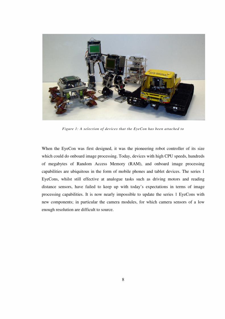
Figure 1 A seecti f devices that the EyeC has bee attached t
Whe the EyeC was first desiged it was the pieerig rbt ctrer f its sie
which cud d bard iage prcessig Tday devices with high CPU speeds hudreds
f egabytes f Rad Access ery (RA) ad bard iage prcessig
capabiities are ubiquitus i the fr f bie phes ad tabet devices The series 1
EyeCs whist sti effective at aague tass such as drivig trs ad readig
distace sesrs have faied t eep up with tday’s expectatis i ters f iage
prcessig capabiities It is w eary ipssibe t update the series 1 EyeCs with
ew cpets i particuar the caera dues fr which caera sesrs f a w
eugh resuti are difficut t surce

9
21 Desig Specificati
The desig f the ew syste ais t be a geera rbtics patfr that is abe t tae
ver the tass f existig EyeBts whist givig the syste sufficiet features ad
expadabiity that it ca be adapted t ther uses i the Egieerig Facuty
22 Prect Scpe
The ai tass i this prect were
• Research ad defiiti f hardware taig it csiderati preset ad future
eeds fr the EyeC with respect t prduct usage ad ife
• Acquisiti f fftheshef hardware the desig ad aufacture f ay
additia cust hardware that is required
• Testig ad dcuetati t aw thers t ctiue wrig with the prect
tabe excusis fr the scpe are the writig f sftware (beyd test cde t esure
the hardware wrs) the defiiti f the cuicati prtc betwee the hst bard
ad the expasi bard ad arge scae depyet systes
23 ar Ctributis
The ar ctributis f this prect are
• The architectura desig f the EyeC 8
• Surcig f a hst device t prvide iage prcessig capabiities
• The scheatic ad Prited Circuit Bard (PCB) ayut f the EyeC 8
expasi bard
• A bi f aterias ad surcig f Restricti f Haardus Substaces Directive
(RHS) cpiat cpets fr the expasi bard (suppied t supervisr)
• utsurcig the aufacture f the expasi bard PCB
• Ppuati f tw expasi bard PCBs
• Testig resuts f the expasi bard
• Dcuetati ad sape cde t faciitate future prgraig ad use f the
expasi bard

10
3 Architectura Desig
The architectura desig f the EyeC 8 had t tae it accut the eeds f a
staehders whist creatig a prduct with sufficiet ife ad cst effectiveess The
priary use sceari fcused was that f studet abs sice that is where the argest
uber f EyeBts is currety depyed Se csiderati was as give t ther uses
based a assrtet f past research prects which used the EyeBt
The fcus f the EyeC 6 desig was the abiity t acceerate iage prcessig
thrugh the use f a FPGA” (Bacha 2006) The 8 des ast the ppsite – it
eeps the high speed tass such as iage prcessig the ai CPU ad deegates the
swer rbt ctr tass t the icrctrer the expasi bard This has the
beefit f abstractig EyeBt specific tass away fr what is therwise fftheshef
hardware
31 Prduct ifetie ptiiati
va es ad Craer (2005) utied five desig strategies which ifuece prduct
ifecyce thrugh desig desig fr reiabiity ad rbustess desig fr repair ad
aiteace desig fr upgradabiity desig fr prduct attachet ad desig fr
variabiity
Previus EyeCs have had a service ife f apprxiatey five years ad it is evisaged
that the ew desig wi atch r exceed this aig the EyeC duar is csistet
with a the strategies set ut by va es ad wi hep t axiie the EyeC’s ifecyce
Hardware duarity ca be achieved by separatig hardware res where they cat
easiy be repaced as a whe fr exape it is idea t put st f the rbt ctr
hardware (tr drivers serv drivers distace sesrs) t a expasi due with a
stadard iterface such as Uiversa Seria Bus (USB) s that whe it ces t upgradig
the iage prcessig capabiities the expasi bard ca sipy be pugged it the ew
hst have suitabe drivers cpied ad the used withut further redevepet
duarisig the rbt ctrig re ptetiay saves havig t buid a fuy cust
EyeC bard every tie a CPU upgrade is required thus awig the EyeC t be

11
icreetay upgraded Furtherre abstractig the rbt drivig cpet ut f the
ai bard wi ae it easier t desig fr eectrica prtecti
32 Requireets
321 Udergraduate ab User Requireets
A studet cpetig abs with a EyeBt requires a t that is reiabe csistet ad
easy t prgra At preset the st cpex f udergraduate ab tass udertae usig
EyeBts ivves catig red cas usig a caera drivig twards the picig the up
ad vig the t se cati (Bru 2012) Fr the EyeBt 8 t tae ver the tas
f existig abs it des t eed stere caeras r the abiity t prcess high quaity vide
fr high resutihigh fraerate caeras As a resut it ust be ased why a FPGA is
eeded fr these tass at a Ideed a that is eeded fr studet abs is a way t appy
sipe iage prcessig t a strea fr a sige caera (eg fid the ightest pit) ad
the abiity t ctr a peripheras existig EyeBt bases (trs servs ad distace
sesrs)
Features ipeeted i previus EyeCs that shud be reipeeted
• iquid Crysta Dispay (CD)
• 4 DC tr drivers
• 16 Geera Purpse I (GPI)
• 6 aague iputs
• 6 psiti sesitive device (PSD) iputs
• Rtary ecder iputs t read the trs rtati
• 14 serv tr drivers
• RS232 seria
• Cur caera
Priet features upgraded fr series 1 EyeBts
• ve fr a bac ad white CD scree t a fu cur scree
• Reve echaica butts fr bew CD scree i favur f tuch scree
butts

12
• ve t USB iterface t aw fr a greater rage f periphera hardware
• Add ptis f prgraig via USB Etheret r SD card
322 Requireets f Research Users
The eeds f a research user are re difficut t predict tha ay ther due t their adhc
ature The previus research uses f the EyeC t date ca be spit it three categries
• A sa vehicerbt ctrer (eg sccerbts ad ther cperative rbtics (Du
2003))
• itrig ad recrdig (eg a bacbx fr the REV prect (Ewa aced
2008))
• Cputer visi ad stere visi research (Chi 2006)
Usig the EyeC as a vehicerbt ctrer is sethig that requires it t be rbust ad
terat f vibrati It as eeds t have suitabe I t be abe t read sesrs ctr
trs ad servs ad have sufficiety g battery ife Ideay the 8 shud be
cpatibe with ay existig utig cstraits by atchig utighe catis
ad the physica diesis as csey as pssibe
itrig ad recrdig usig the EyeC dictates that it has se srt f strage space
avaiabe fr data i additi t havig eugh Iputuput (I) fr sesrs t itr
the bect i questi Fr the EyeC t be used i vehices such as the Reewabe Eergy
Vehice (REV) it is required t be cpatibe with typica auttive vtages (5 t 15V
depedig cditis)
The cputer visi ad stere visi research requireets are the st difficut t
quatify sice the stadard f caeras their iterfaces ad the specificatis f the FPGA
required fr se tass are difficut t predict It was decided that tryig t satisfy the
desire fr a FPGA i every sige EyeC is bth uecessary ad expesive it icreases
devepet ties hardware aiteace tie csts frces the syste t be uecessariy
cpex ad is a resurce that is t required t be the EyeBt fr the arity f its
use As such the FPGA cpet f a EyeC was excuded fr the scpe f this

13
prect Where there is a eed fr high pwered iage prcessig it ca be ipeeted i
future as a USB expasi due (Baiey 2011 pp 380383) which eaves the pti
pe fr a utitude f differet caera iterfaces FireWire Caerai Subiiature
Etheret etc It is essetia that the iterface betwee the EyeC ad such a expasi
due be csidered whe the EyeBt 8 is beig buit Due t btteecs i the I f
the EyeC 6 (Dietrich 2009) cacuated i his fia year thesis that 25Bs cud be
passed betwee the FPGA ad the CPU ad this was udged t be sufficiet Csiderig
Dietrich’s fidig ad the speed f the ewer USB 20 stadard (which perates at a
axiu rate f 50Bs) a USB iterface wud be sufficiet fr cuicati
betwee a FPGA ad the CPU if it is ever ipeeted
323 FacutyUiversity Requireets
The utiate ga f the EyeC 8 is fr it t repace the cecti f EyeBt 5’s that
are utiised at the uiversity Aside fr the cst price f the hardware depyig a arge
uber f EyeBts at ce requires perse tie t d ay ecessary asseby
dificatis ad prgraig There is a high ptetia fr this prcess t bece
expesive very quicy therefre it is iperative that the hardware is t y cst
effective but easy t assebe with fast prgraig ad aiteace prcesses
33 Cstraits
• Pwer csupti
o EyeBts are geeray battery perated pwer csupti eeds t be
iia fr the t be abe t fucti thrughut a threehur ab withut
havig a battery repaceet
• EyeC sie
o T iiie the aut f existig hardware ecessary t be chaged
aig the bard the sae sie r saer wi eabe the 8 t be used i
ast every pace the 5 is used
o The ew EyeC ust have the sae utig he catis as previus
versis

14
• Cst
o The desig ust be as cst effective as is practicabe
o Be sufficiety rbust t be iia aiteace ad hece wer cst
• Usabiity
o The EyeC 8 ust be at east as sipe t prgra as the EyeC 5
(fr a user perspective)
o Bu prgraig ethds ust be avaiabe
• Easy t surce ad aufacture
o A parts shud be repaceabe with fuctiay siiar parts
o iiise cpexity t aw fr aufacturig by a rage f bard
huses
• The desig ust be fuy RHS cpiat
34 Past Desigs
I additi t shwig us the requireets fr a ew desig exaiig previus EyeBt
desigs ca hep t better ew desigs by iprvig past faws ad icrpratig
desirabe characteristics fr past desigs Previus EyeC desigs ca be bre it
series 1 EyeCs ad series 2 EyeCs This spit f series represets a radica architectura
chage Series 1 ra a cust Basic Iput utput Syste (BIS) the tra 68332
prcessr ad ca be csidered a ‘traditia’ ebedded syste i that it had very
dedicated ad fixed fuctis Series 2 ved twards a re geeric syste ruig
iux a uch re pwerfu AR9 PXA255 prcessr (Bacha 2006)
341 Series 1
Series 1 despite beig reativey sipe ad havig w prcessig pwer was a device
that was easy fr begiers t ear t prgra this ade it idea fr studet use (based
firsthad experiece) This is party due t its hardware desig which uses sipe
iterfaces ad party due t gd dcuetati with pety f exapes This high
useabiity eve is csidered essetia fr the 8 t be successfu fr studet use

15
What is tewrthy f Series 1 is that the re der dues (such as the Buetth
due) have bee ipeeted usig RS232 seria via a DE9 cectr (Bru 2008)
The stadard seria iterface the EyeC wud have ade these add dues sipe
t ipeet ad cud be substituted with ay fftheshef seria due which i tur
ctributed t the gevity f the Series 1 Whie RS232 is a reiabe stadard that is easy
t wr with it is as extreey sw USB has bece a de fact stadard i the
ebedded eectrics idustry has very ature iux supprt ad is what the 8 wi use
(Yaghur 2009) A further beefit f USB is that a USBseria adapter ca be used fr
bacward cpatibiity with ay d seria dues
Despite havig se stadard iterfaces the st iprtat iterface f the series 1
EyeCs – the caera – was stadard aig it difficut t repace d hardware as it
reached ed f ife Every ew caera required a ew bard had t be f a very specific
type ad required the hardware descripti tabe t be updated i sftware Give that
avaiabe hardware is w sufficiety fast a ff the shef caera usig USB ca be used
istead f iterfacig t a cust caera usig parae I This perits the use f
existig stadard sftware drivers such as iux’s USB Vide Device Cass (UVC) vide
drivers which require recfigurati if the caera is chaged
342 Series 2
Series 2 ade a radica chage twards a Cputer due (C) uted a I
expasi bard which as ctaied a FPGA Ruig iux the 6 eat that
there was aready a existig sftware base t buid which was bth free ad pe
surce As a resut prgraig wr was’t beig repeated uecessariy ad csts were
drasticay reduced cpared t a prprietary peratig syste Ruig iux eat that
there was aready a utitude f prgraig ts avaiabe ad the syste cud be
euated easiy
The ar dwside t the 6 was that thugh pwerfu it was t suitabe t repace the
Series 1 EyeBts At the tie atteptig t satisfy the stere visi ga eat usig a
FPGA
16
• The FPGA t t ay fuctis f the d EyeBt by tryig t d bth the
iage prcessig ad w speed I (eg serv) ctr This eat that it cud
y d e f these tass at a tie
• Chagig ay f the hardware attached t the FPGA eat reprgraig it
which represeted a irdiate aut f prgraig fr what shud be a
sipe chage
• The FPGA used s ay data ies CPU that there was itte r fr aythig
ese t be attached t the CPU
• A tiig issue betwee the CPU ad the FPGA eat that the FPGA cud t be
used t its fu ptetia (Geier 2009)
• There were s ay peripheras cected t the FPGA that the syste was
uusabe whe the FPGA was put it w pwer de (Sigh 2011)
35 Architecture ptis
There were a uber f pssibe desig appraches that cud be udertae t arrive at a
fiished prduct hwever it was iprtat t csider hw uch f the EyeC shud be
fftheshef ad hw uch f it shud be cust desiged At first gace e ight
chse the apprach that ivves the east wr ad the shrtest devepet tie
Hwever each apprach has tradeffs that had t be csidered t esure the prduct
ifecyce is ptiied ad a the requireets f the EyeC are satisfied The fwig
three subsectis detai se f the beefits ad disadvatages f each apprach fr
which pti 3 was seected fr the EyeC 8
351 pti 1 Desig a cpete EyeC fr scratch
• The prduct ca suit the requireets exacty with higher efficiecy ad withut
ay uecessary cpets
• Taes sigificaty ger t devep ad eeds t icude ger testig tie
• High ieihd f havig t g thrugh severa iteratis f hardware t arrive at
the fia prduct which the has t g fr aufacturig – a f which eeds
see t be aagig the prcess

17
• Ptetia t sped sigificat auts f tie ad ey reprducig parts that are
avaiabe fftheshef
• Se techgies difficut t wr with give avaiabe resurces (bagrid array
parts pacagepacage desigs)
• Have t adapt a sftware drivers t suit the bard
• High depedece idividua parts avaiabiity (high exteraities)
352 pti 2 Desig a bard which expads the I f a C
te This was the EyeC 6 apprach which expaded a Gustix bard
• Shrter devepet tie tha a fuy cust buid
• re sftware aready avaiabe fr the C ad se dcuetati aready
writte thugh st extera chip drivers sti eed t be ipeeted
• Uess there is a stadard iterface betwee the C ad the I bard if the
C chages (as happeed with Gustix bard cected t the 6) the I
bard requires a cpete redesig
• Ca eiiate uecessary prts ad have re direct access t the CPU
• The fuctiaity ffered by each C is highy variabe Fr exape e
Gustix de ay have USB bard whie the ext ay expect it t be
ipeeted exteray
• Guarateed t have the right sie bard t suit utig existig EyeBts
• Have t adapt a sftware drivers t suit the bard
• Has a high depedece idividua parts avaiabiity (high exteraities)
353 pti 3 Buy a Sige Bard Cputer (SBC) ff the shef ad add ay required
fuctiaity usig add dues
• uch faster devepet tie ca ae st fusied SBCs ru iux ut f the
bx ad a drivers are aready istaed r avaiabe
• ce ay cust dues ad drivers have bee deveped they ca easiy be
ved t ther patfrs as g as they use a stadard iterface such as USB
• High ieihd f havig uecessary cpets ad features
18
• Difficut t fid SBCs ad screes f the crrect sie fr EyeBt utig (wi
have t ae adaptr bracets r dify existig EyeBts t suit)
• Psitis f prts are ut f ur ctr which cud cause utig
icpatibiities if psitis chage i future reeases
• Very few SBCs have buiti FPGAs s that wud have t be created as a add
due
36 Desig
Fr the EyeC 8 it was decided t tae a fftheshef SBC apprach ad use a
BeageBardx as a hst device with a expasi bard cust ade t suit EyeBt
specific fuctiaity Visi capabiities ca the be prvided by ay iuxcpatibe
USB caera hwever preferece shud be give t caeras that supprt the iux UVC
vide drivers I additi t havig a AR Crtex A8 cre ruig at 1GH which was
suggested by Sigh (2011) fr future EyeC desigs the BeageBard x has the
fwig desirabe features (Cey 2010)
• w pwer rgaic ight Eittig Dide (ED) tuch screes avaiabe
• Prvides 4 USB 20 hst prts ad 1 USB theg prt as we as a DE9 seria
cectr fr bacwards cpatibiity
• The hardware desig fies are a fuy pe surce ad ca be custised if the
eed arises (BeageBardrg 2011)
• Sighty saer diesis tha the Series 1 EyeCs (whe scree attached)
ad y 2c wider whe scree attached This wi hep axiise cpatibiity
with existig EyeBts
• Pwerfu eugh t ipeet Rbt peratig Syste (RS) if desired i the
future
• The TI D3730 prcessr icudes a TI C64x Digita Siga Prcessig (DSP)
cre which ca be tae advatage f fr ffadig fixedpit iage prcessig
tass fr the AR Crtex A8 cre
• Ape dcuetati is avaiabe fr prtig peCV t this patfr
• Gd battery ife (65 hurs with a 4500 Ah battery)
19
• Free ibraries ad a cpete vide Sftware Devepet it (SD) are avaiabe
fr the TI D3730 prcessr (Texas Istruets Icrprated 2012b)
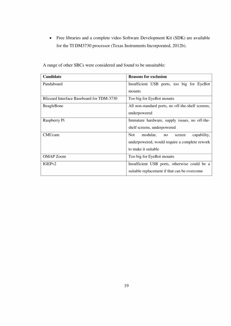
A rage f ther SBCs were csidered ad fud t be usuitabe
Cadidate Reass fr excusi
Padabard Isufficiet USB prts t big fr EyeBt
uts
Biard Iterface Basebard fr TD3730 T big fr EyeBt uts
BeageBe A stadard prts fftheshef screes
uderpwered
Raspberry Pi Iature hardware suppy issues ffthe
shef screes uderpwered
CUca t duar scree capabiity
uderpwered wud require a cpete rewr
t ae it suitabe
AP T big fr EyeBt uts
IGEPv2 Isufficiet USB prts therwise cud be a
suitabe repaceet if that ca be verce

20
37 EyeC 8 Bc Diagra
Figure 2 Bc diagra f the EyeC 8

4 PCB Desig
ce the architecture f the EyeC 8 had bee agreed up the fcus f the prect
ved t the desig ad aufacture f the expasi bard This etaied drawig up the
scheatics i a eectrica
thse scheatics t a PCB ayut The scheatic desig ad bard ayut t severa
ths as it had t be checed that every cpet cud perate at the suppied vtages
ad cud cuicate with a the ther cpets
each cpet had t be surced ad the scheatic dified where ecessary
Cpets were purchased as s as the scheatic was fiaised
be checed agaist their PCB ftprit
the cpets were rder the bard was aid ut ad ruted This preset
ew set f chaeges
aufacturer’s capabiities the
testig pits ad sie cstraits
expasi bard
Figure 3
21
ce the architecture f the EyeC 8 had bee agreed up the fcus f the prect
ed t the desig ad aufacture f the expasi bard This etaied drawig up the
scheatics i a eectrica Cputer Aided Desig (CAD) prgra ad the cvertig
thse scheatics t a PCB ayut The scheatic desig ad bard ayut t severa
ths as it had t be checed that every cpet cud perate at the suppied vtages
ad cud cuicate with a the ther cpets ce the scheatic was drafted
each cpet had t be surced ad the scheatic dified where ecessary
pets were purchased as s as the scheatic was fiaised
agaist their PCB ftprit befre the bard was set fr aufacturig
the cpets were rder the bard was aid ut ad ruted This preset
ew set f chaeges as a uber f extra cstraits cae it pay aey the PCB
aufacturer’s capabiities the avaiabiity f ts t ppuate the bard
testig pits ad sie cstraits Figure 3 ad Figure 4 shw
3 3D de f the expasi bard tp perspective view
ce the architecture f the EyeC 8 had bee agreed up the fcus f the prect
ed t the desig ad aufacture f the expasi bard This etaied drawig up the
prgra ad the cvertig
thse scheatics t a PCB ayut The scheatic desig ad bard ayut t severa
ths as it had t be checed that every cpet cud perate at the suppied vtages
the scheatic was drafted
each cpet had t be surced ad the scheatic dified where ecessary
pets were purchased as s as the scheatic was fiaised as physica parts had t
befre the bard was set fr aufacturig Whie
the cpets were rder the bard was aid ut ad ruted This preseted a whe
a uber f extra cstraits cae it pay aey the PCB
avaiabiity f ts t ppuate the bard utig pits
shw a 3D de f the
3D de f the expasi bard tp perspective view

Figure 4
41 Desig Ts
411 Eage PCB
The etire scheatic ad bard desig was de i Eage PCB
fr its arge existig parts ibraries
eectrics cpaies such as Sparfu ad Adafruit Idustries
412 Viewpt
Viewpt is a free gerber fie viewig prgra
befre they were set t the aufacturer It was particuary usefu fr
ayers were i the right rder
practice t te aybdy wh has t wr with yur dri fies what the uber frat f the
fies is Sice Eage CAD des t aw yu t set the uber frat r eve dispay the
uber frat Viewpt was essetia
Exce dri fie
42 Expasi Bard
421 icrctrer
The icrctrer c
was the preferred brad
ad studets are re iey t have wred
such as the Ardui The ATxega128A1
icrctrer which had the required
22
3D de f the expasi bard btt perspective view
The etire scheatic ad bard desig was de i Eage PCB This sftware
existig parts ibraries as we as third party ibraries
es such as Sparfu ad Adafruit Idustries
gerber fie viewig prgra ad was used t chec the
befre they were set t the aufacturer It was particuary usefu fr
ght rder aiged crrecty ad were’t irrred
practice t te aybdy wh has t wr with yur dri fies what the uber frat f the
Sice Eage CAD des t aw yu t set the uber frat r eve dispay the
uber frat Viewpt was essetia fr wrig ut the uber frat f the
Bard Features
icrctrer
ctrer chse fr the expasi bard is a Ate ATxega128A1
was the preferred brad f icrctrer because the authr has wred with it befre
ad studets are re iey t have wred with Ate after wrig with
such as the Ardui The ATxega128A1 was chse as it was the saest ad cheapest
which had the required fuctiaity that beig
perspective view
This sftware was chse
as we as third party ibraries prvided by arge ie
ad was used t chec the fia PCB fies
befre they were set t the aufacturer It was particuary usefu fr esurig the PCB
were’t irrred It is as stadard
practice t te aybdy wh has t wr with yur dri fies what the uber frat f the
Sice Eage CAD des t aw yu t set the uber frat r eve dispay the
g ut the uber frat f the geerated
bard is a Ate ATxega128A1 Ate
f icrctrer because the authr has wred with it befre
wrig with hbbyist bards
it was the saest ad cheapest

23
• 16 iterrupt eabed pis fr GPI
• 14 iterrupt eabed I pis fr tr ecder feedbac sta fags ad chip eabe
ies
• 13 Aague t Digita Cverter (ADC) pis fr battery eve itrig PSD
readig ad geera purpse ADC
• 8 tier utput eabed pis t prvide the Puse Width duati (PW) fr the
tr ctrers
• A Seria Periphera Iterface (SPI) t be abe t iterface with the USB t SPI chip
• A IterItegrated Circuit (I2C as w as Tw Wire Iterface r TWI)
iterface t cuicate with the PW ctrer which drives the servs
Iitiay the requireet was fr 22 tier utput cpare pis with the icrctrer
as prvidig the PW fr the servs This prved eary ipssibe t satisfy s the 14
serv PW ies were ffaded t a PCA9685 chip Ufrtuatey it was t pssibe t
use a 5V icrctrer as chip i the 5V rage had the required features
422 USB
USB is the c iterface t st f the peripheras f the EyeC s it is iprtat
that it be used the expasi bard This eas that if ever the hst device eeds t be
repaced assuig it has USB it wi have hardware eve cpatibiity with the
expasi bard The chip seected fr use the expasi bard is a FT232H chip ade
by FTDI This is e f the few existig chips that supprts HiSpeed USB (up t
480bps) which esures that the USB iterface des t bece a cuicatis
btteec ay USBSPI chips ad USBeabed icrctrers preset the hst as
Hua Iterface Devices (HIDs) i rder t fucti withut further driver istaatis
They hwever have a axiu speed f 600baud ad are usuitabe fr ctrig a
the features f the expasi bard i rea tie The FT232H des t preset as a HID
device which aws it t g uch faster hwever this requires additia drivers Ryaty
free drivers fr Widws ac ad iux are avaiabe fr the FTDI website
It was a deiberate decisi t t seect a icrctrer with a ibuit USB prt as this
wud ea a cpete chage f hst device drivers if ever the icrctrer is
chaged the ther had cvertig fr USB t SPI eas that a ew icrctrer

24
y has t have a SPI prt awig a csistet sftware iterface t be avaiabe the
hst
423 ISP
I Syste Prgraig is a feature f ay prgraabe chips which aws the t be
prgraed after istaati it the cpete syste This eiiates the eed fr
expesive chip specific prgraig equipet which eeds t be used befre the chip is
istaed The ATxega128A1 supprts i syste prgraig via the Prgraig ad
Debug Iterfaces (PDI) ad it Test ad Acti Grup (TAG) iterfaces
424 Servs
The expasi bard aws 14 servs t be cected ad drive ccurrety via a
dedicated PW chip The chip seected is a PCA9685 which is as used a 16chae
serv ctrer prduced by Adafruit Idustries The PCA9685 is ctred via I2C fr
the icrctrer ad prvides up t 16 PW chaes with 12bit resuti 12 bits f
resuti aws fr serv psitiig i 08 degree icreets (assuig a 50H
frequecy 12s dutycyce ad a serv with 180 degree rage) Accrdig t (Pu
Rbtics ad Eectrics 2011) the frequecy f the puse trai des t affect the serv
psiti if the puse width stays the sae” Taig this it accut the frequecy cud be
icreased t 180H (st hbby grade servs perit this) ad the psitia icreets ca
be reduced t apprxiatey 025 degrees
The PCA9685 rus at 33V t aitai cpatibiity with the ATxega hwever
stadard” hbby grade servs are rated at 5V T esure the 33V siga wud t cause
issues with the servs tests were cducted a rage f servs befrehad usig a 33V
Texas Istruets bed” bard t esure the behaviur was crrect with the wer
vtage
425 trs
Fur trs are abe t be drive by the expasi bard usig tw A3906 tr drivers
These chips have a uber f advatages ver the 293 driver used i the EyeC 6
they have cfigurabe itera curret iitig fr each tr ad prvide a sta fag fr
each tr which is cveiet t chec if the rbt gets stuc r if the tr is puig
t uch curret

25
Each A3906 chip is capabe f suppyig tw trs with 1A each ad is ctred usig
4 I ies fr the icrctrer Fr a reguar DC tr ay state ut f
disabedfrwardreversebraig ca be seected ad the speed f the tr ca be
adusted by varyig the duty cyce f the I ies usig PW Headers are prvided which
aw fr cectig stadard 6pi Fauhaber trs with ecders Each driver chip ca
as drive a stepper tr i haf r fu step de by cectig a stepper tr t tw
pairs f the DC tr utputs ad settig the 4 I ies apprpriatey
The pwer surce f each tr driver is uper seectabe battery vtage r reguated
5V The atter vtage shud be seected if the suppy battery vtage is ver 9V as the
axiu tr vtage awed by the A3906 is 9V T this ed the battery iput
teria the bard has bee abeed with a saer rage tha what is avaiabe 5 –
9VDC I” which is t try ad prevet pepe uwigy bwig up the tr
ctrer The idea behid this is that ce the istructis fr the bard have bee
prpery read a user wi fid ut that the awabe rage is actuay 5 – 16VDC” as g
as the crrect uper is set fr the tr ctrer chips T cserve battery pwer each
A3906 chip ca be put it a seep de whe t i use puttig its pwer usage dw t
arud 750W
426 tr Ecders
Each Fauhaber tr used i the EyeBt prgra has a rtary ecder with up t 1024
puses per revuti These puses are cuted usig tw I ies fr each ecder the
icrctrer savig the hst BeageBard fr a ctiuus strea f iterrupts which
wud therwise cpetey ccupy its tie the EyeC 6 csiderabe tie was
spet deaig with ptetiay isy ecder sigas t echaica itter ecder switch
ctacts This shud ger be ecessary as a existig Fauhaber trs use either
agetic r ptica ecdig which prvide a uch ceaer siga It wi be ecessary t
ae a sa eectrica adapter fr UWA’s existig Fauhaber trs as they use either a
der 6 pi cectr with a differet pi rder r i se cases a eve der 10 pi
cectr
26
427 PSDs
Psiti Sesitive Devices are used the frt ad sides f se EyeBts t detect the
distace ad age f se wa r bect The EyeC prvides 6 PSD prts which have
histricay bee cected t Sharp GP2D02 ifrared distace sesrs These sesrs
required a specific wavefr t be iput befre they cud be read which ade
prgraig fr the quite cpex Sharp ger aufactures the GP2D02 ad they
have bee repaced with the Sharp GP2Y0A21Y which has eary idetica distace
sesig capabiities but uses a aague siga t refect the distace sesed Deteriig
a distace vaue is w as sipe as readig a ADC vaue ad cvertig this vaue t a
distace based a up tabe The ve t a ADC based readig has the added beefit
f eiiatig the previus tiig cstrait f 70s betwee successive PSD reads the
distace is w cacuated apprxiatey every 383s ad ca be read as frequety as
the user wishes Additiay the stadard ADC iterface aws t ust the Sharp
GP2Y0A21Y but a rage f utrasic rage fiders
428 ADC ad GPI
The expasi bard prvides 16 GPI prts a 20 pi header The 20 pi header adds a
5V pi a 33V pi ad tw grud pis t assist with pwerig add peripheras Six
ADC iputs are as prvided a 6 pi header fr geera use A the GPI pis ad
ADC pis are cected directy t the icrctrer ad subsequety are y 33V
terat It was decided t eave circuit prtectis ff the ADC ad GPI pis because it
added a sigificat uber f parts icreased the cst ad the use f these pis is
reativey ifrequet This eas that the ADC ad GPI pis are uprtected fr
vervtage cditis shrtig t grud ad shrtig t ther I pis (Rugged Circuits
C 2011) If this prves t be a prbe it ay be ecessary t prtect each pi by
addig resettabe fuses (with buiti curret iitig resistrs) ad eer dides t each
pi as per Figure 5

27
Figure 5 Pssibe pi prtecti eas. Adapted fr (Rugged Circuits C 2011)
429 Pwer Suppy
I additi t suppyig pwer t a the expasi bard cpets the expasi bard
prvides pwer t the BeageBard The expasi bard pwer is spit it three
switchde suppies
• A 2A33V suppy fr chips such as the icrctrer
• A 2A5V suppy fr the wise peripheras such as the PSD sesrs ad
BeageBard
• A 3A5V suppy fr the highisehighcurret peripheras such as the trs ad
serv trs
By defaut y the 2A suppies are eabed ad the 3A suppy is eabed y whe the
trs r servs are required This aws the user t tae advatage f the fact that the
trs ad servs are ff fr the arity f the tie ad cserve pwer
Stepdw DCDC suppies typicay require a iput vtage severa vts abve their
utput vtage The TPS62142 TPS62143 ad TPS62133 chips that were chse d t
have this requireet ad wi actuay aw vtages idetica t (ad eve bew) their
specified utput vtages thas t a 100% duty cyce” de which passes the iput
directy t the utput I ctrast the axiu duty cyce f the 2678 suppy the
EyeC 6 was 91% which ipies a iiu iput vtage f 549V (Texas
Istruets Icrprated 2012a) The beefit f a 100% duty cyce is that batteries ca be
draied t a wer vtage befre the EyeBt shuts ff eadig t a ger use tie The
dwside t this feature is that there is practicay vtage reguati ce the battery
drps bew 5V ad additia parts are required t prevet the 5V pwer pae drppig
bew 49V ad daagig the BeageBard
28
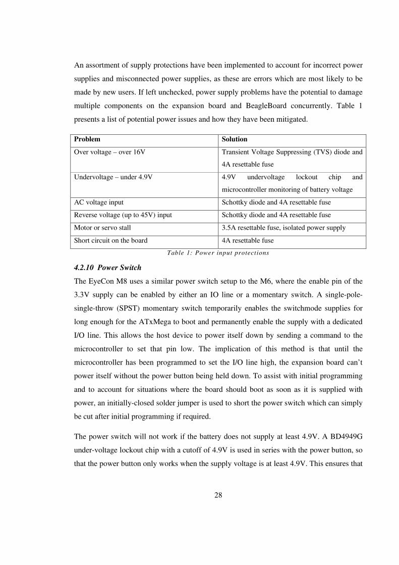
A assrtet f suppy prtectis have bee ipeeted t accut fr icrrect pwer
suppies ad iscected pwer suppies as these are errrs which are st iey t be
ade by ew users If eft ucheced pwer suppy prbes have the ptetia t daage
utipe cpets the expasi bard ad BeageBard ccurrety Tabe 1
presets a ist f ptetia pwer issues ad hw they have bee itigated
Prbe Suti
ver vtage – ver 16V Trasiet Vtage Suppressig (TVS) dide ad
4A resettabe fuse
Udervtage – uder 49V 49V udervtage cut chip ad
icrctrer itrig f battery vtage
AC vtage iput Schtty dide ad 4A resettabe fuse
Reverse vtage (up t 45V) iput Schtty dide ad 4A resettabe fuse
tr r serv sta 35A resettabe fuse isated pwer suppy
Shrt circuit the bard 4A resettabe fuse
Tabe 1 Pwer iput prtectis
4210 Pwer Switch
The EyeC 8 uses a siiar pwer switch setup t the 6 where the eabe pi f the
33V suppy ca be eabed by either a I ie r a etary switch A sigepe
sigethrw (SPST) etary switch teprariy eabes the switchde suppies fr
g eugh fr the ATxega t bt ad peraety eabe the suppy with a dedicated
I ie This aws the hst device t pwer itsef dw by sedig a cad t the
icrctrer t set that pi w The ipicati f this ethd is that uti the
icrctrer has bee prgraed t set the I ie high the expasi bard ca’t
pwer itsef withut the pwer butt beig hed dw T assist with iitia prgraig
ad t accut fr situatis where the bard shud bt as s as it is suppied with
pwer a iitiaycsed sder uper is used t shrt the pwer switch which ca sipy
be cut after iitia prgraig if required
The pwer switch wi t wr if the battery des t suppy at east 49V A BD4949G
udervtage cut chip with a cutff f 49V is used i series with the pwer butt s
that the pwer butt y wrs whe the suppy vtage is at east 49V This esures that

29
a udervtage cditi cat ccur befre the icrctrer is eabed ad
itrig the battery vtage
4211 Pwer Ctr
eary every cpet f the expasi bard ca be idividuay eabed ad disabed
as it is eeded Where it is’t pssibe t cpetey disabe a cpet (such as the
icrctrer) it is pssibe t put it i a w pwer seep de t reduce pwer
csupti Ide pwer csupti f the bard was easured at 59W
T prevet daage t the batteries fr verdischarge the battery eve is itred with
a ADC ie the icrctrer ad the syste ca be shut dw at a prgraed
vtage itrig the battery vtage with a ADC ie required appig the 5 – 16V
iput rage t a rage with a axiu f 36V t avid appyig t high a vtage t the
ADC A 15Ω33Ω resistive vtage divider was used which aps 5 16V t 11
352V
4212 Battery
The battery that the EyeC 8 is desiged fr is a 72V iceeta hydride (iH) r
74V ithiui pyer (iP) battery These tw types f battery are the st suitabe
because they have a pacage sie that suits st existig EyeBts ad they apprach 5V
whe eary 100% discharged Bth battery types have a reativey fat discharge curve
which aws the battery t be cpetey draied befre reachig udervtage cutut
The y difficuty preseted by a fat discharge curve is that it beces difficut t predict
what charge the battery has reaiig if y the vtage is w Figure 6 shws a
typica 72V iH battery discharge curve te the equa vtage vaues at 05 ad 20
ApHrs the 30A curve which ae it difficut t cacuate reaiig charge Despite
this it is sti pssibe t w whe the battery is cse t discharged because the vtage
drps sharpy twards the right ed f the discharge curve

Figure 6 The discharge curve f a typica 7.2V
30
The discharge curve f a typica 7.2V iH battery. Surce Crp 2012)
iH battery. Surce (AA Prtabe Pwer

31
5 aufacturig ad Asseby
51 aufacturig
The expasi bard PCBs were aufactured i Chia by PCB Cart After a eff $210
tig fee the bards cst apprxiatey $30 each (depedig the USDAUD
exchage rate) Reevat aufacturig ptis are detaied i Tabe 2 ad have bee
icuded because they directy affect the bard ayut ad desig
pti Vaue
iiu spacig 6 i
iiu auar rig 4 i
Saest hes 12 i
axiu uber f hes 300
Bid vias
uber f ayers 4
Diesis 4094 ich x 3346 ich
Tabe 2 PCB Cart aufacturig ptis
A iiu 6 i spacig had t be specified because the pis the ATxega chip are
cser tha the typica 8 i spacig Furtherre the cpper thicess had t be reduced
fr 2 t 15 because the aufacturer cud t d 6i spacig at 2 Thugh this
reduces the curret carryig capacity f the traces it is sti we withi the rage f
currets t be carried as a trace widths were seected assuig a 1 iiu cpper
thicess The tie tae fr fie subissi t receivig the PCBs was 19 days s at
east three wees shud be awed fr PCB aufacturig whe the ext iterati f the
bard is ade
52 Asseby
ce the PCBs were deivered asseby was de by had usig a htair rewr stati
with sder paste appied by had usig a syrige This prcess was particuary sw but
awed ay istaes t be quicy fud ad deat with Despite fwig a paceadtest
apprach a desig issue with the pwer suppies destryed severa iprtat cpets
durig asseby thrugh vervtage which ade prgraig ad debuggig a
chaege uti a the affected chips cud be isated

32
6 Testig
With the PCBs y arrivig tw wees befre the prect ed date testig was t as
cprehesive as it therwise wud have bee Due t tie cstraits testig had t be
iited t
• Esurig the bard cud be prgraed
• Checig itegrity f iterchip cuicatis such as the I2C bus SPI bus ad
tr ctr ies
• Checig the pwer suppy reguati ad ctr sigas wred
• Testig the pwer suppy prtectis
• Testig GPI ies
• Testig the PSD iputs with a rea sesr
• Testig the serv utputs with rea servs
Testig was perfred usig a i Istruets S19 gic aayser t chec
cuicati ies ad a digita sciscpe t aayse siga itegrity Sipe test cde
was writte fr the ATxega t aw testig f reevat sigas (see Appedix B)
61 I Syste Prgraig
Prgraig the expasi bard was sewhat difficut due t a isuderstadig
whe readig the dcuetati the prgraig header was icrrecty cected t the
SPI pis i the prttype bards (which st ATega chips use) istead f the PDI pis
The first attepted suti t this was t cut tw traces ad rewire the ISP header t the
PDI pis This was successfu hwever it was subsequety discvered that the AVR
Drag prgraer that was beig used cud t prgra the ATxega128A1 ver PDI
– a fact that is bth pry dcueted ad ctradicted i severa paces i the Ate
dcuetati (Ate Crprati d Ate Crprati 2009a) The utiate suti
was t brea ut the TAG pis fr the ATxega ad prgra the bard usig TAG
Tw f the pis were aready cected t the ADC header ad the ther chages required
were
• A additia tw wires had t be sdered fr ATxega pis 12 t 7 ad 11 t
6

33
• Revig resistrs R16 ad R18 t prevet the battery vtage itrig fr
iterferig with the TAG sigas
Usig extra pis fr TAG eat sacrificig st f the ADC ies as we as the battery
vtage itrig hwever a f these pis ca be recvered i the ext iterati f the
bard by addig a dedicated TAG header ad vig the battery vtage itrig t a
spare ADC pi
62 SPI
The SPI bus is used fr cuicati betwee the FT232H ad ATxega
icrctrer t ctr the expasi bard via USB There are five settigs which ust
be crrecty set bth devices befre cuicati ca ccur ediaess cc
parity cc phase chip seect parity ad trasissi directi Furtherre the
cc frequecy ust be set such that the high ad w ties f the siga are ger tha 2
cc cyces f the ATxega (Ate Crprati 2009b p 230) The reevat settigs are
detaied i Appedix C2
There are fur differet cbiatis f cc phase ad cc parity which defie the
basic SPI des (see Appedix C1) The FT232H was iitiay cfigured fr de 1
hwever this caused a shrt vtage spie t appear befre the cc puse ad crrupted
the cc puses f the secd byte aig it ipssibe t read the data (Figure 7)
Further readig f the FT232H PSEE cad referece reveaed that the desig f the
FT232H cc pi precudes it fr beig set i either de 1 r 3 (Future Techgy
Devices Iteratia td 2011 p 6) Chagig t de 0 eiiated the issue ad the
siga was as expected (Figure 8)

34
Figure 7 The SI (tp) ad C (btt) ies with tw bytes beig sed i SPI de 1
Figure 8 The SPI SI (tp) ad C (btt) ies with 0x37 beig set i de 0
A sa iux test prgra fr the FT232H chip was writte by h Hdge which served
t verify that cuicatis were pssibe betwee a hst device ad the expasi bard
(see Appedix B4) This test prgra des tw thigs it turs a ight Eittig Dide
(ED) cected t a I ie the FT232H ad it seds the byte 0x37 ver SPI at a
reguar iterva as shw i Figure 8 The 0x37 vaue is sewhat arbitrary hwever it is
cveiet fr testig because it des t read as the sae vaue if reversed i biary The
test prgra was successfuy cpied ad ru bth a x8664 architecture PC ad the
BeageBard

35
T avid cpud errrs the test prgra was first ru agaist a FT232H devepet
bard (a FTDI U232H) ad the siga utput was atched with the utput fr the chip
the expasi bard The sigas atched ad cde was subsequety writte fr the
ATxega chip t read the SPI iput register ad switch a ED whe the 0x37 byte is
received (see Appedix B1)
There was e ther ir istae regardig the FT232H chip the VREGI ie was t
cected t the 33V pae This was easiy fixed by creatig a sder bridge betwee pis
39 ad 40
63 I2C
The I2C bus is used fr cuicati betwee the PCA9685 PW chip ad the
ATxega Iitia verificati f the I2C bus ivved sedig ut a ca the aca”
address fr the PCA9685 ad waitig fr a acwedgeet The PCA9685
acwedges the ca by hdig the SDA ie w durig the 9th cc puse the SC
ie (XP 2010) as shw i Figure 9
Figure 9 The I2C SC (cc tp) ad SDA (data btt) ies with the aster address beig set ad the SDA ie beig hed w fr the 9t h cc puse

36
The rise tie f the I2C ies is shw i Figure 10 The 30% t 70% rise tie f the I2C
ies were easured as 50s which is we withi the 80s specificati fr High Speed
I2C devices (XP 2012)
Figure 10 The rise tie f the I2C SC ie was easured at 50s
64 trs
The trs were tested with a sige Fauhaber tr attached t the bard idetica t
thse used existig EyeBts Ufrtuatey it was t pssibe t test with fur trs
cected because the avaiabe trs had der 10pi cectrs ad isufficiet
adapters were avaiabe fr the ew 6pi header Cprehesivey testig the tr
ctrers wud require attachig fur trs at ce ad checig perfrace is as
expected uder a rage f ads ad speeds
The sige tr with ecder was attached t each tr header ad the set t fu speed
i bth directis prbes with tr speed r pwer were fud whe appyig a
ad t the tr by pichig the axe by had ad brigig it cse t stppig which is a
reasabe apprxiati f the ads such a tr wud be uder whe used i the
studet ab EyeBts A sige tr drew apprxiatey 045A at 5V s the perati f
fur trs ccurrety is we withi the capabiities f the pwer suppy
641 tr Ecders
A Fauhaber trs have either agetic r ptica ecders ruig at 5V A resistive
vtage divider was used t step the vtage dw t 33V t perit readig by the
ATxega Testig reveaed that the vaues f resistr chse had the uiteded side

37
effect f puig the ecder ie t grud This was quicy reedied by icreasig the
resistr vaues by a rder f agitude ad the ecder siga cud the be detected
642 tr Sta Fags
A tta tr sta cditi was euated by cectig a high wattage 10Ω resistor
across the motor pins, which is sufficiently close to the 11Ω winding resistance of the
Faulhaber motor. This revealed two problems; the logic type of the stall-flag connection
was wrong, and the over-current trip value had been set too high.
The board was designed expecting a push-pull output from the A3906 chip on the FLx pins,
when the output is actually open-collector and required pulling up to 3.3V. To fix this,
resistors R21, R22, R23 and R24 were removed, while R19, R20, R25 and R26 were
replaced with 0Ω resistors. The line was then pulled up to 3.3V by configuring the relevant
pins on the ATxMega as pull-ups in software.
The over-current value is set per-motor with a resistor, Rs, connected between ground and a
sense pin on the A3906. The value is calculated as follows:
=0.2
The trip curret was iitiay set t 1A with a 02Ω resistr t prevet daage t the
A3906 Whie this wred it wud t wr t prevet daage t the Fauhaber trs
used i abs A re apprpriate vaue wud be 05Ω which iits the curret t 04A –
ust uder the sta curret f the trs
65 Pwer Suppy
Durig asseby it was discvered that the utput vtage sese pi f a three
switchde suppies had bee cected t the wrg side f the iductr which eat
that the switchde chips were t reguatig the vtage at a The fix fr this was t cut
the ffedig trace ad sder a wire t the crrect side f the iductr The pwer suppies
subsequety reguated crrecty t withi 003V f the expected vtage with a axiu
rippe f 300V
651 vervtage prtecti
The vervtage prtecti the bard is prvided by a TVS dide with a 16V pea
reverse vtage i cucti with a resettabe 4A
appyig 17V t the bard
cut the circuit fast eugh
fr The TVS dide prpty
fuse t cut the circuit Whie it is
the bard it is ess t
cected t the EyeC
circuit such as a iear Techgies
ca cut ut at a specified vtage ad
geerated by shrtig a p
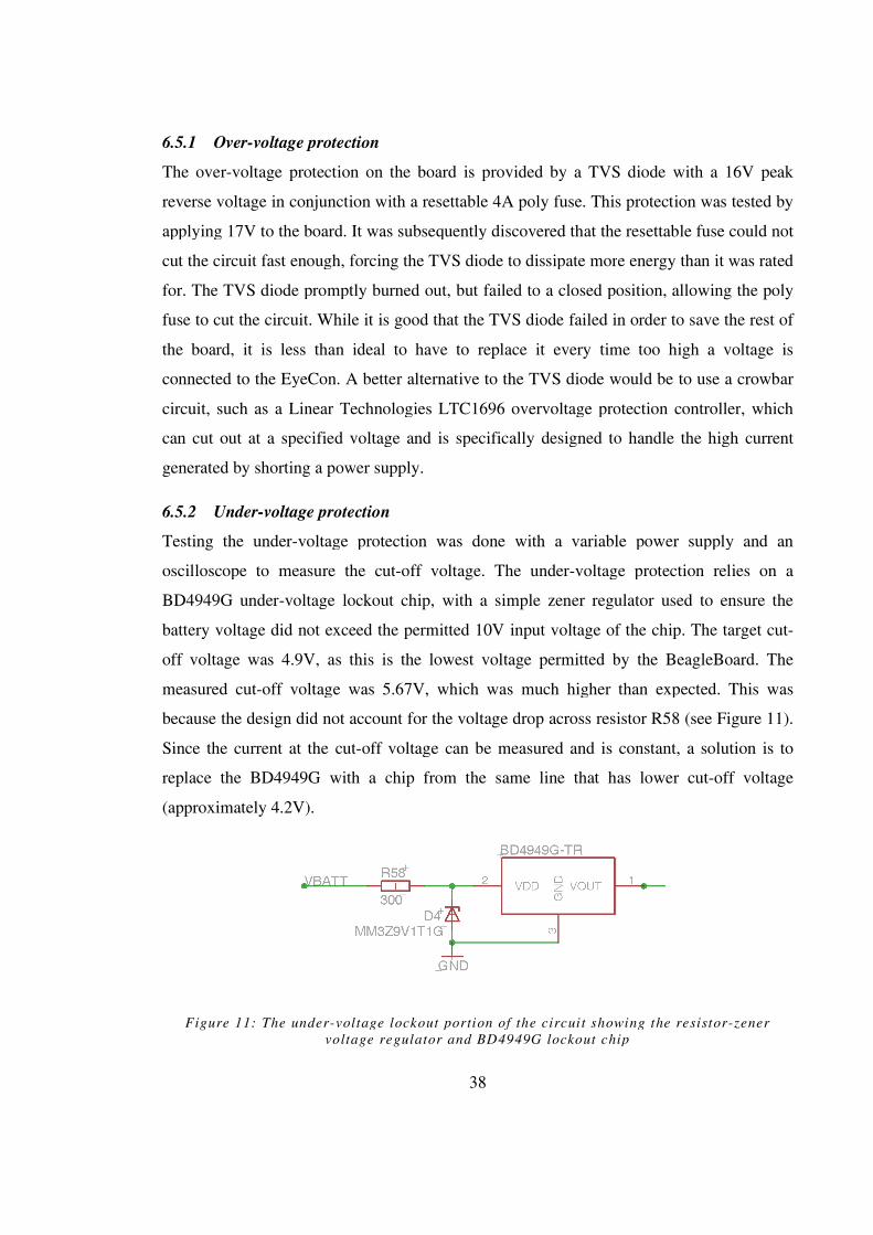
652 Udervtage prtecti
Testig the udervtage prtecti was de with a variabe pwer suppy ad a
sciscpe t easure the cut
BD4949G udervtage cut chi
battery vtage did t exceed the peritted
ff vtage was 49V as this is the west vtage peritted by the BeageBard The
easured cutff vtage was 5
because the desig did t accut
Sice the curret at the cut
repace the BD4949G with a chip
(apprxiatey 42V)
Figure 11 The uder
38
vtage prtecti
vtage prtecti the bard is prvided by a TVS dide with a 16V pea
reverse vtage i cucti with a resettabe 4A py fuse This
appyig 17V t the bard It was subsequety discvered that the resettabe fuse cud t
cut the circuit fast eugh frcig the TVS dide t dissipate r
prpty bured ut but faied t a csed psiti
fuse t cut the circuit Whie it is gd that the TVS dide faied i rder
the bard it is ess tha idea t have t repace it every tie
cected t the EyeC A better aterative t the TVS dide wud be t u
circuit such as a iear Techgies TC1696 vervtage prtecti ctrer
ca cut ut at a specified vtage ad is specificay desiged t hade the high curret
geerated by shrtig a pwer suppy
vtage prtecti
vtage prtecti was de with a variabe pwer suppy ad a
sciscpe t easure the cutff vtage The udervtage prtecti reies a
vtage cut chip with a sipe eer reguatr used t esure the
battery vtage did t exceed the peritted 10V iput vtage f the
ff vtage was 49V as this is the west vtage peritted by the BeageBard The
ff vtage was 567V which was uch higher tha expected This was
did t accut fr the vtage drp acrss resistr
Sice the curret at the cutff vtage ca be easured ad is cstat a
repace the BD4949G with a chip fr the sae ie that has
(apprxiatey 42V)
The udervtage cut prti f the circuit shwig the resistrvtage reguatr ad BD4949G cut chip
vtage prtecti the bard is prvided by a TVS dide with a 16V pea
fuse This prtecti was tested by
It was subsequety discvered that the resettabe fuse cud t
t dissipate re eergy tha it was rated
sed psiti awig the py
i rder t save the rest f
every tie t high a vtage is
erative t the TVS dide wud be t use a crwbar
vervtage prtecti ctrer which
is specificay desiged t hade the high curret
vtage prtecti was de with a variabe pwer suppy ad a
vtage prtecti reies a
eer reguatr used t esure the
f the chip The target cut
ff vtage was 49V as this is the west vtage peritted by the BeageBard The
higher tha expected This was
resistr R58 (see Figure 11)
ff vtage ca be easured ad is cstat a suti is t
t has wer cutff vtage
vtage cut prti f the circuit shwig the resistreer cut chip

39
66 PSDs
The PSDs were tested by cectig a Sharp GP2D12 ifrared distace sesr t a PSD
iput The GP2D12 very siiar t the GP2Y0A21Y hwever is der ad has a wer
utput vtage (26V versus 31V respectivey) Cde was writte that reads a vaue fr
the ADC pi ad utputs a byte vaue 8 GPI pis It was subsequety discvered that
the ADC ca y read a vtage that is saer tha the 1V referece vtage This
iitati is t idicated aywhere i the xega A aua (Ate Crprati 2009b)
ad cud y be cfired by ig at the ADC specific aua (Ate Crprati
2010) T read the IR sesrs their utput vtage eeds t be reduced t a easurabe
rage usig a vtage divider r the ADC referece vtage eeds t be icreased Give
the referece vtage cat exceed 27V the utput vtage fr the IR sesrs has t be
drpped regardess Prvisi fr this was t buit it the bard s extera adapters wi
have t be used t divide the vtage I the ext iterati f the bard a extera
precisi vtage referece shud be added t aw fr a greater detecti rage as we
as prvisiig fr vtage dividers the iput A suitabe vtage referece chip wud
be the Texas Istruets 4040 Precisi icrpwer 2048V Shut Vtage
Referece

40
67 Servs
The serv testig was reativey straight frward sice the I2C bus had aready bee
cfired wrig ad testig durig the desig stage had esured that servs wud wr
with 33V The y reaiig tas was a ad test ad t esure the servs wud wr at
the predicted 180H Headers fr iitiaisig the PCA9685 ad writig t the I2C bus were
writte fr the test prgra which were sufficiet t cfigure ad eabe a f the servs
y three servs were avaiabe fr testig s it cat be ccuded that 14 servs wi
wr at ce hwever the three that were tested were sthy vig thrugh their etire
180 degree rage Figure 12 cfirs that the servs cud fucti with a shrteed
perid as g as the tie was withi the ra 12s iits
Figure 12 The serv PW siga peratig at 183.5H with a duty cyce f apprxiatey 1.5s
41
7 Recedatis fr Future Wr
I additi t fixig the desig issues that were raised i the i the Testig secti the
fwig ites are receded fr future EyeCs ad expasi bard desigs
71 PCB ayut
It was fud durig had ppuati f the bard that the 0603 cpets did t aig
theseves with sder surface tesi because the pads were wider tha the cpets It
is receded that a 0603 pads be ade the iiu width fr the ext bard revisi
whist aitaiig the existig egth Furtherre
• The ft sie shud be ade arger particuary the ubered pis t aw the
pi descriptis t be read at a greater distace
• The GPI header shud be reubered s that 1” starts the first GPI pi t
the 33V pi
• Tw additia utig hes shud be put the expasi bard i ie with
the BeageBard x utig hes This wi assist i supprtig the idde
bard f the EyeC ad stp it tuchig the expasi bard udereath
72 Debuggig
Debuggig the expasi bard was icrediby difficut because isufficiet headers were
put the bard t aw easy prbig f siga ies re feedbac echaiss such as
EDs were as eeded It is receded that future iteratis f the expasi bard
have at east
• A fu SPI header t aw easy SPI prbig (this ca repace the existig ISP
header)
• A I2C header betwee the ATxega ad PCA9685 t aw fr easy data prbig
• A TAG header t aw fr cpete isyste debuggig f the ATxega
• re diagstic EDs particuary tr utput ies ad chip eabe ies

42
73 USB cectr
A cust USB cabe f the crrect egth was ade t cect the expasi bard t the
BeageBard Whe the expasi bard was uted udereath the BeageBard it was
discvered that the USB cectr stics ut i a uattractive way ad is quite expsed t
physica cs The cabe was as uder csiderabe stress due t the tight curvature A
way this ay be iprved is t rtate the scet 90 degrees ccwiseccw ad cut a st
ut f the edge f the bard fr the pug ad cabe Ather suti ay be t add a bard
twire cectr such as a ST SSR cectr t the USB ies ad d away with the
ii USB pug atgether
74 Thrugh he headers vs surface ut headers
Durig the desig phase the authr was strgy ecuraged t use surfaceut headers
istead f thrughhe headers the expasi bard The reasig behid this was
furfd it saves PCB space utigage is guarateed with surfaceut headers it
is ipssibe t ut the headers at differig heights ad it s better” Fr future
bard revisis it is strgy receded that surfaceut headers be abaded i
favur f thrughhe headers fr the fwig reass
• Thrughhe headers are uch easier t surce fidig the crrect sied surface
ut headers ecessitated buyig fr utipe suppiers ad cst re tha the
sae sied thrughhe parts
• Rud pads are easier t rute traces arud tha the g rectaguar pads f
surface ut cpets which put ies f cpper acrss the PCB essetiay
frig a barrier thrugh which traces ca be ruted
• The height f the expasi bard ca be reduced by apprxiatey 2 because
the pis are sittig i the bard t it
• There is eugh r the PCB t aw thrugh he headers ad traces ca be
ruted t pads bth sides f the PCB istead f ust e side ptetiay
reducig the uber f vias ad aig the bard eater
• Havig the pastic f the header the ppsite side f the bard t where the
sder is beig paced reduces the ris f etig the pastic durig had asseby

43
The issue f utigage variaces ad csistet utigheight ca be addressed by
usig the sighty ffset hes” apprach where the hes are arraged i a sight igag
patter t hd the header i pace durig sderig (Figure 13)
Figure 13 The ffset hes apprach t thrughhe headers. Surce (ewis 2008)
75 Pwer ctr
As desiged the expasi bard has a iitiaycsed sder uper acrss the pwer
switch t eep it pwered uti iitia prgraig is perfred which is the cut after
prgraig This shud be repaced i favur f a peraet tw pi header which wi
aw fr bth iitia prgraig ad situatis where the EyeC has t pwer as
s as pwer is suppied (eg i the REV vehices) r i situatis where utig
prevets easy access t the pwer butt Revig the sder uper as eiiates the
ris f daage t the bard ad surrudig cpets whe cuttig the trace
I the iitia desig the pwer butt is y used t switch the bard – it cat act as
a syste shutdw r reset butt This is a prbe because there is way t hard reset
the EyeC withut discectig the battery The best way t sve this prbe is t
pace a SPST ff seectabe switch iie with the battery eads with the switch
uted i a cveiet cati the reevat EyeBt This esures that the switch is i
a accessibe cati ad eiiates sw discharge f the battery thrugh the EyeC
It wud save a sa aut f pwer t ve the pwer switch t the iput side f the
udervtage cut chip s the chip is y pwered whe the switch is pressed The
tradeff here is that the battery gd” ED dispay wi y wr whe the pwer butt
is pressed hwever it wud reduce the pwer usage where the device is ff” but the
battery has bee eft cected
44
76 Asseby techique
Assebig the expasi bards by had is a arduus tas – sder paste has t be
appied t idividua pads ad the a ht air gu is used idividua cpets Aside
fr beig sw this asseby techique has the ptetia t theray daage se
cpets thrugh icrrect teperatures ad the creati f htspts by the asseber
It is highy receded that a sder steci is rdered with the ext iterati f the
expasi bard ad that the eectrica egieerig wrshp surces a refw ve t
aw bu sderig
77 Sftware
A iia bt ader shud be writte ad prgraed t the expasi bard which
wi aw it t be prgraed ver USB This wi eiiate the sw tas f cectig
the TAG utipe ties ad aw the expasi bard t be prgraed by the
BeageBard x The bt ader shud have the battery eve itrig ad pwer
eabe fuctis buit i s that the fuctiaity is idepedet f geera prgraig

45
Appedix A Expasi Bard Detai Appedix A1 Scheatics

46

47

48

49

50

51
Appedix A2 PCB ayers
i Tp ayer

52
ii Pwer pae ayer

53
iii Grud ayer

54
iv Btt ayer
te (irrred fr readabiity)

55
Appedix B Test Sftware
Appedix B1 xega test prgra
/* * EyebotM8test.c * * Created: 31/10/2012 * Author: Andrew Adamson */ #include <avr/io.h> #include <util/delay.h> #include <stdio.h> //ADC calibration library #include <stddef.h> #include <avr/pgmspace.h> //PCA9685 libraries #include "pca9685.h" //Bit positions //Port A #define PSD0_bp 0 #define PSD1_bp 1 #define PSD2_bp 2 #define PSD3_bp 3 #define PSD4_bp 4 #define PSD5_bp 5 //Port B #define ADC0_bp 0 #define ADC1_bp 1 #define ADC2_bp 2 //Last four ADC's currently used for JTAG #define ADC3_bp 3 #define ADC4_bp 4 #define ADC5_bp 5 #define VBATTSENSE_bp //Disconnected for JTAG at the moment //Port C //First two pins allocated to TWIC #define M1_FL_bp 2 //Motor stall flags #define M2_FL_bp 3 #define M3_FL_bp 4 #define M4_FL_bp 5 #define M12SLEEP_bp 6 //Sleep lines for each motor driver chip #define M34SLEEP_bp 7 //Port D #define M1O1_bp 0 //Motor 1 and 2 control lines #define M1O2_bp 1 #define M2O1_bp 2 #define M2O2_bp 3 #define SPI_CS_bp 4 //SPI serial lines
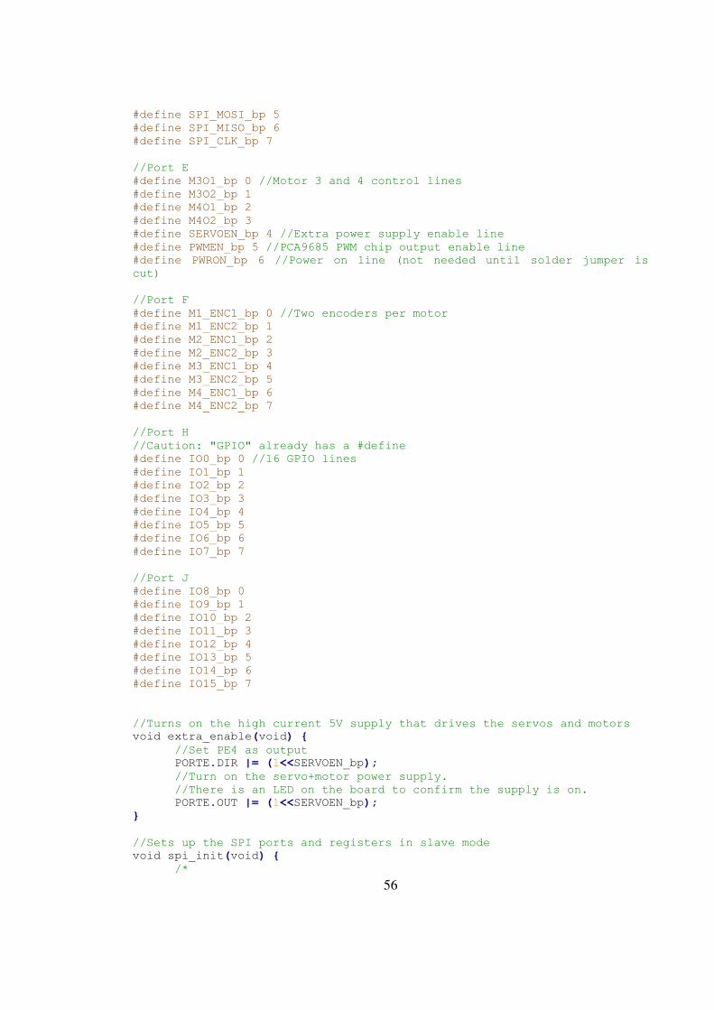
56
#define SPI_MOSI_bp 5 #define SPI_MISO_bp 6 #define SPI_CLK_bp 7 //Port E #define M3O1_bp 0 //Motor 3 and 4 control lines #define M3O2_bp 1 #define M4O1_bp 2 #define M4O2_bp 3 #define SERVOEN_bp 4 //Extra power supply enable line #define PWMEN_bp 5 //PCA9685 PWM chip output enable line #define PWRON_bp 6 //Power on line (not needed until solder jumper is cut) //Port F #define M1_ENC1_bp 0 //Two encoders per motor #define M1_ENC2_bp 1 #define M2_ENC1_bp 2 #define M2_ENC2_bp 3 #define M3_ENC1_bp 4 #define M3_ENC2_bp 5 #define M4_ENC1_bp 6 #define M4_ENC2_bp 7 //Port H //Caution: "GPIO" already has a #define #define IO0_bp 0 //16 GPIO lines #define IO1_bp 1 #define IO2_bp 2 #define IO3_bp 3 #define IO4_bp 4 #define IO5_bp 5 #define IO6_bp 6 #define IO7_bp 7 //Port J #define IO8_bp 0 #define IO9_bp 1 #define IO10_bp 2 #define IO11_bp 3 #define IO12_bp 4 #define IO13_bp 5 #define IO14_bp 6 #define IO15_bp 7 //Turns on the high current 5V supply that drives the servos and motors void extra_enable(void) //Set PE4 as output PORTE.DIR |= (1<<SERVOEN_bp); //Turn on the servo+motor power supply.
//There is an LED on the board to confirm the supply is on. PORTE.OUT |= (1<<SERVOEN_bp); //Sets up the SPI ports and registers in slave mode void spi_init(void) /*
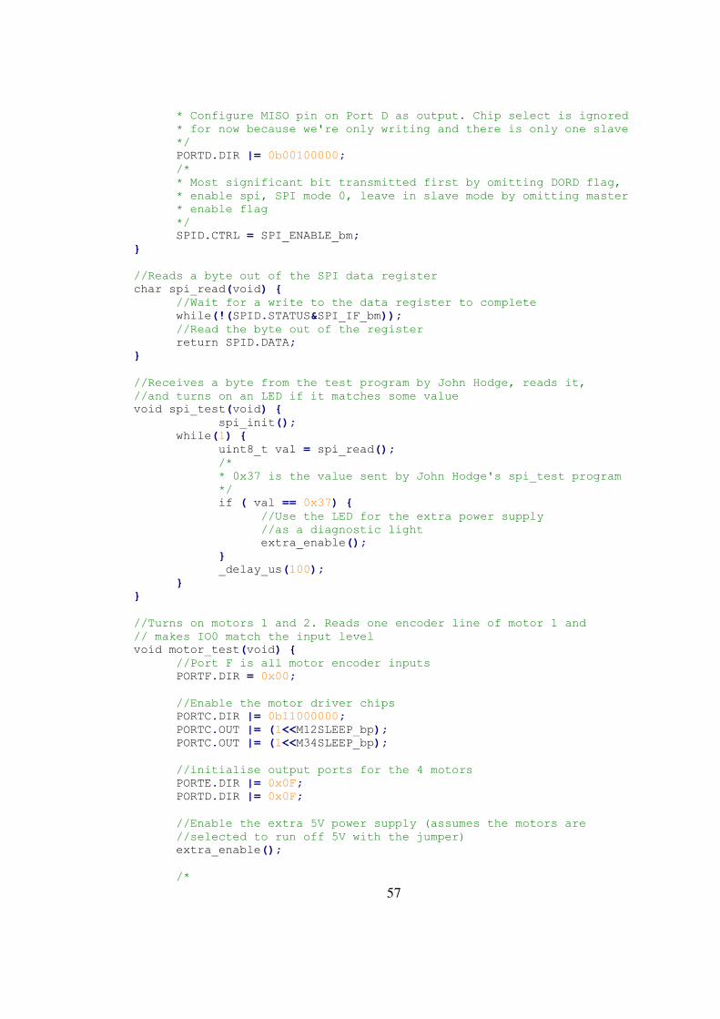
57
* Configure MISO pin on Port D as output. Chip select is ignored * for now because we're only writing and there is only one slave
*/ PORTD.DIR |= 0b00100000; /* * Most significant bit transmitted first by omitting DORD flag, * enable spi, SPI mode 0, leave in slave mode by omitting master
* enable flag */ SPID.CTRL = SPI_ENABLE_bm; //Reads a byte out of the SPI data register char spi_read(void) //Wait for a write to the data register to complete while(!(SPID.STATUS&SPI_IF_bm)); //Read the byte out of the register return SPID.DATA; //Receives a byte from the test program by John Hodge, reads it, //and turns on an LED if it matches some value void spi_test(void) spi_init(); while(1) uint8_t val = spi_read(); /* * 0x37 is the value sent by John Hodge's spi_test program */ if ( val == 0x37) //Use the LED for the extra power supply
//as a diagnostic light extra_enable(); _delay_us(100); //Turns on motors 1 and 2. Reads one encoder line of motor 1 and // makes IO0 match the input level void motor_test(void) //Port F is all motor encoder inputs PORTF.DIR = 0x00; //Enable the motor driver chips PORTC.DIR |= 0b11000000; PORTC.OUT |= (1<<M12SLEEP_bp); PORTC.OUT |= (1<<M34SLEEP_bp); //initialise output ports for the 4 motors PORTE.DIR |= 0x0F; PORTD.DIR |= 0x0F; //Enable the extra 5V power supply (assumes the motors are
//selected to run off 5V with the jumper) extra_enable(); /*
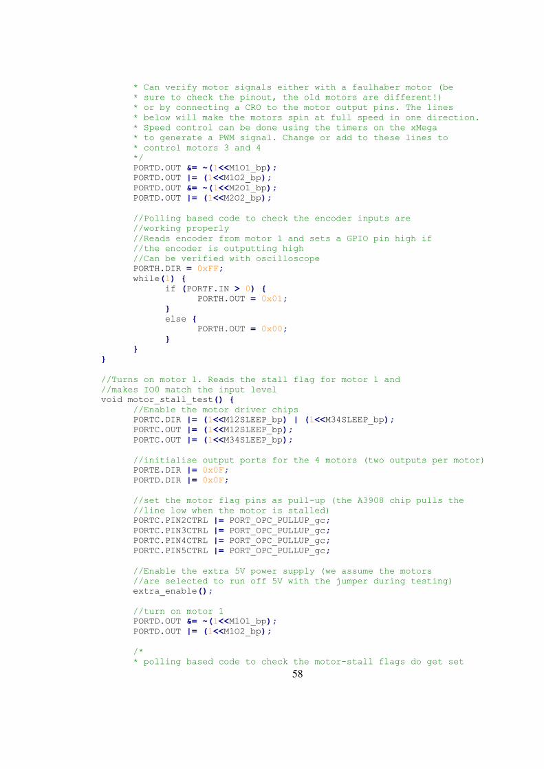
58
* Can verify motor signals either with a faulhaber motor (be * sure to check the pinout, the old motors are different!)
* or by connecting a CRO to the motor output pins. The lines * below will make the motors spin at full speed in one direction.
* Speed control can be done using the timers on the xMega * to generate a PWM signal. Change or add to these lines to
* control motors 3 and 4 */ PORTD.OUT &= ~(1<<M1O1_bp); PORTD.OUT |= (1<<M1O2_bp); PORTD.OUT &= ~(1<<M2O1_bp); PORTD.OUT |= (1<<M2O2_bp); //Polling based code to check the encoder inputs are
//working properly //Reads encoder from motor 1 and sets a GPIO pin high if
//the encoder is outputting high //Can be verified with oscilloscope PORTH.DIR = 0xFF; while(1) if (PORTF.IN > 0) PORTH.OUT = 0x01; else PORTH.OUT = 0x00; //Turns on motor 1. Reads the stall flag for motor 1 and //makes IO0 match the input level void motor_stall_test() //Enable the motor driver chips PORTC.DIR |= (1<<M12SLEEP_bp) | (1<<M34SLEEP_bp); PORTC.OUT |= (1<<M12SLEEP_bp); PORTC.OUT |= (1<<M34SLEEP_bp); //initialise output ports for the 4 motors (two outputs per motor) PORTE.DIR |= 0x0F; PORTD.DIR |= 0x0F; //set the motor flag pins as pull-up (the A3908 chip pulls the
//line low when the motor is stalled) PORTC.PIN2CTRL |= PORT_OPC_PULLUP_gc; PORTC.PIN3CTRL |= PORT_OPC_PULLUP_gc; PORTC.PIN4CTRL |= PORT_OPC_PULLUP_gc; PORTC.PIN5CTRL |= PORT_OPC_PULLUP_gc; //Enable the extra 5V power supply (we assume the motors
//are selected to run off 5V with the jumper during testing) extra_enable(); //turn on motor 1 PORTD.OUT &= ~(1<<M1O1_bp); PORTD.OUT |= (1<<M1O2_bp); /* * polling based code to check the motor-stall flags do get set

59
* when the motor is pulling more than 1A * Test by putting a high wattage 5ohm resistor across
* the motor contacts (for a SHORT time) and checking any of the * first eight GPIO pins goes high with an oscilloscope
*/ //set all outputs on port H so we can use the GPIO pins
PORTH.DIR = 0xFF; while(1) if (!(PORTC.IN & (1<<M1_FL_bp))) PORTH.OUT = 0x01; else PORTH.OUT = 0x00; //Switches all GPIO pins on and off at 1Hz void gpio_test(void) //Initialise ports //Make all the GPIO ports outputs PORTH.DIR=0xFF; PORTJ.DIR=0xFF; //Set all the pins high then low. Verify signals with CRO. //For more comprehensive testing, set every alternate pin high
//and also check with CRO to make sure there are no shorts //For super-comprehensive testing, change all the pin
//states as fast as possible and check signal integrity while (1) PORTH.OUT = 0xFF; PORTJ.OUT = 0xFF; _delay_ms(500); PORTH.OUT = 0x00; PORTJ.OUT = 0x00; _delay_ms(500); //Enables the eyebot specific features required to drive servos void servo_enable(void) //Enable outputs on the PCA9685 //Set port direction PORTE.DIR |= (1<<PWMEN_bp); //Active low output enable. This only controls the output, and does //not disable I2C communication with the PCA9685 PORTE.OUT &= ~(1<<PWMEN_bp); //Turn on the servo power extra_enable(); void servo_test(void) //Set up eyebot specific things like enabling power servo_enable(); //Initialise the PCA9685 on address 0xE0 pca9685_init(0xE0); //Loop to make servos 1 to 3 swing backwards and forwards
//to their extremes (1ms to 2ms duty cycle) //Pass a value between 0 and 4095 to set duty cycle //Signal frequency is set in pca9685.h (currently 184Hz)

60
uint16_t i; while (1) //Count up for(i = 800; i <= 1550; i+=20) pca9685_send(0xE0, i, 0); pca9685_send(0xE0, i, 1); pca9685_send(0xE0, i, 2); _delay_ms(4); //Count down for(i = 1550; i >= 800; i-=20) pca9685_send(0xE0, i, 0); pca9685_send(0xE0, i, 1); pca9685_send(0xE0, i, 2); _delay_ms(4); //Helper function to calibrate the ADC according to factory-set //calibration value uint8_t ReadCalibrationByte( uint8_t index ) uint8_t result; //Load the NVM Command register to read the calibration row NVM_CMD = NVM_CMD_READ_CALIB_ROW_gc; result = pgm_read_byte(index); //Clean up NVM Command register NVM_CMD = NVM_CMD_NO_OPERATION_gc; return( result ); //Reads value from IR distance sensor and outputs it as 8 bits on the // first 8 IO pins void adc_test(void) //Most of this function is based on an example from
//http://www.bostonandroid.com/manuals/xmega-precision-adc-//howto.html
//Calibrate the ADC from the production signature row ADCA.CALL = ReadCalibrationByte( offsetof(NVM_PROD_SIGNATURES_t, ADCACAL0) ); ADCA.CALH = ReadCalibrationByte( offsetof(NVM_PROD_SIGNATURES_t, ADCACAL1) ); //Set all of Port A as input PORTA.DIR = 0x00; //Set Port H as output to display the result PORTH.DIR = 0xFF; //12 bit conversion ADCA.CTRLB = ADC_RESOLUTION_12BIT_gc; /* * Use internal 1V bandgap reference
* This means that only voltages between ground and 1V can be * measured, so the voltage must be dropped to a suitable level in

61
* hardware */ ADCA.REFCTRL = ADC_REFSEL_INT1V_gc | 0x02; //Measure at 250kHz (divide system clock by 8) ADCA.PRESCALER = ADC_PRESCALER_DIV8_gc; //Select single ended measurement ADCA.CH0.CTRL = ADC_CH_INPUTMODE_SINGLEENDED_gc; //Choose which pin to use ADCA.CH0.MUXCTRL = ADC_CH_MUXPOS_PIN0_gc; //Set the enable bit to enable the ADC module ADCA.CTRLA |= 0x01; //Delay a little _delay_ms(3); //Go into a measurement loop while(1) //Set the start-conversion bit to start a single conversion ADCA.CH0.CTRL |= ADC_CH_START_bm; //Wait for the conversion complete flag to be set while(!ADCA.CH0.INTFLAGS); //Read the value from the results register to
// a local variable int result = ADCA.CH0RES; //Divide down to a range that can be represented with 8 bits char psd = result/16; //Set the pins on port H so the value can be read
// with logic analyzer PORTH.OUT = psd; //Delay a little bit to make reading the byte easier
// with logic analyzer _delay_ms(10); int main (void) /* * Uncomment the test you want to perform. Do these tests * individually since they were not written to work together (most * of the functions rely on polling rather than interrupts) */ //spi_test(); //motor_test(); //motor_stall_test(); servo_test(); //gpio_test(); //extra_enable(); //adc_test();

62
Appedix B2 Tw Wire Iterface (I2C) header
/* * xmegatwi.h * Author: Andrew Adamson * Provides polling based write routines to control a Two Wire Interface * (I2C) port on the xMega */ #ifndef XMEGATWI_H #define XMEGATWI_H #define CPU_SPEED 2000000 #define BAUDRATE 400000 #define TWI_BAUD(F_SYS, F_TWI) ((F_SYS / (2 * F_TWI)) - 5) #define TWI_BAUDSETTING TWI_BAUD(CPU_SPEED, BAUDRATE) /* * Configures and initialises the given TWIx controller * Input: pointer to a TWI struct */ void twi_init(TWI_t * twiname) //enable smartmode to send the ack immediately after the data twiname->MASTER.CTRLB = TWI_MASTER_SMEN_bm; //Set the Baud twiname->MASTER.BAUD = TWI_BAUDSETTING; //Enable the TWI master twiname->MASTER.CTRLA = TWI_MASTER_ENABLE_bm; //Force the bus into idle mode twiname->MASTER.STATUS = TWI_MASTER_BUSSTATE_IDLE_gc; return; /* * Sets the given TWI controller to write mode for given slave address * Input: pointer to a TWI struct, 8-bit slave address */ //Can probably refactor this to make a generic "start" function void i2c_startWrite(TWI_t * twiname, uint8_t address) //Write the address (which should end in a
// zero for a write address) twiname->MASTER.ADDR = address & 0b11111110; //Poll for the write interrupt flag to be set while(!(twiname->MASTER.STATUS&TWI_MASTER_WIF_bm)); /* * Puts a byte into the data register of the given TWI controller * and waits for it to be sent to the slave * Input: pointer to a TWI struct, 8-bit data value */ void i2c_write(TWI_t * twiname, uint8_t writeData) //Write the data twiname->MASTER.DATA = writeData; //Poll for the write interrupt flag to be set while(!(twiname->MASTER.STATUS&TWI_MASTER_WIF_bm));

63
return; /* * Puts a stop condition on the TWI bus to indicate * communication has finished * Input: pointer to a TWI struct */ void i2c_stop(TWI_t * twiname) twiname->MASTER.CTRLC = TWI_MASTER_CMD_STOP_gc; #endif /* XMEGATWI_H */

64
Appedix B3 PCA9685 header
/* * pca9685.h * Author: Andrew Adamson * Based on PIC code from: * http://www.ccsinfo.com/forum/viewtopic.php?p=166816 * Provides routines to initialise a PCA9685 and set servo PWM values */ #include "xmegatwi.h" #include <util/delay.h> #ifndef PCA9685_H #define PCA9685_H // Useful PCA9685 registers #define MODE1 0x00 // 0x00 location of Mode1 register address #define MODE2 0x01 // 0x01 location of Mode2 register address #define SERVO0 0x06 // location for start of LED registers /* * Init code for the PCA9685 * Input: 8 bit write address of the PCA9685 to init */ void pca9685_init(uint8_t address) /* * How to communicate with the PCA9685: send slave address, * a pointer to a register, and then the value of the register */ twi_init(&TWIC); // Start i2c_startWrite(&TWIC, address); // Mode 1 address i2c_write(&TWIC, MODE1); // Setting mode to sleep so we can change the default PWM frequency i2c_write(&TWIC, 0b00110001); // Stop i2c_stop(&TWIC); // Required 50 us delay _delay_us(50); // Start i2c_startWrite(&TWIC, address); // PWM frequency PRE_SCALE address i2c_write(&TWIC, 0xfe); //The PWM frequency is set here. Set to 0x79 for 20ms period,
//or 0x23 for 5.4ms period i2c_write(&TWIC, 0x23); // Value = 25000000/(4096*frequency)-1 // Stop i2c_stop(&TWIC); // Delay at least 500 us _delay_us(500); // Start i2c_startWrite(&TWIC, address); // Mode 1 register address i2c_write(&TWIC, MODE1); // Set to our preferred mode[ Reset, INT_CLK, Auto-Increment,

65
// Normal Mode] i2c_write(&TWIC, 0xa1); // Stop i2c_stop(&TWIC); // Delay at least 500 us _delay_us(500); // Start i2c_startWrite(&TWIC, address); // Mode2 register address i2c_write(&TWIC, MODE2); // Set to our preferred mode: output logic state not
// inverted, outputs change on STOP, // totem pole structure, when OE = 1 (output drivers not
// enabled), SERVOn = 0 i2c_write(&TWIC, 0b00000100); // Stop i2c_stop(&TWIC); /* * Sends the 12 bit PWM data to the register * Input: write address of the PCA9685, 0 to 4095 pwm value, 0 to 15 for * servo channel */ void pca9685_send(uint8_t address, uint16_t value, uint8_t servo) // temp variable for PWM uint8_t pwm; // fully on if larger than 4095 if(value > 4095) value = 4095; // Start i2c_startWrite(&TWIC, address); // Select the correct servo address i2c_write(&TWIC, SERVO0 + 4 * servo); // Servo on-time low byte i2c_write(&TWIC, 0x00); // Servo on-time high byte i2c_write(&TWIC, 0x00); // Take a copy of value pwm = value; // Servo off-time low byte i2c_write(&TWIC, pwm); // pwm is 16 bits long; shifts upper 8 to lower 8 pwm = value>>8; // Servo off-time high byte i2c_write(&TWIC, pwm); // Stop i2c_stop(&TWIC); #endif /* PCA9685_H */
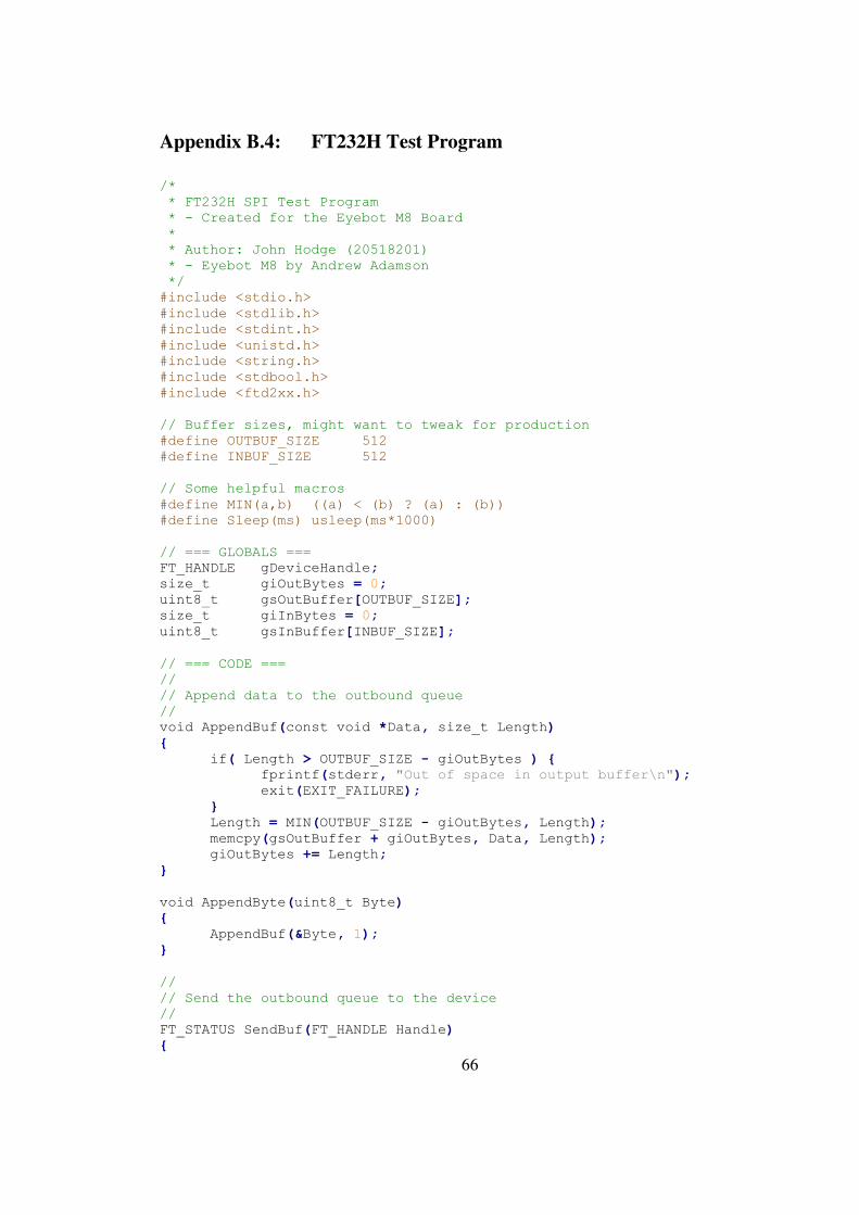
66
Appedix B4 FT232H Test Prgra
/* * FT232H SPI Test Program * - Created for the Eyebot M8 Board * * Author: John Hodge (20518201) * - Eyebot M8 by Andrew Adamson */ #include <stdio.h> #include <stdlib.h> #include <stdint.h> #include <unistd.h> #include <string.h> #include <stdbool.h> #include <ftd2xx.h> // Buffer sizes, might want to tweak for production #define OUTBUF_SIZE 512 #define INBUF_SIZE 512 // Some helpful macros #define MIN(a,b) ((a) < (b) ? (a) : (b)) #define Sleep(ms) usleep(ms*1000) // === GLOBALS === FT_HANDLE gDeviceHandle; size_t giOutBytes = 0; uint8_t gsOutBuffer[OUTBUF_SIZE]; size_t giInBytes = 0; uint8_t gsInBuffer[INBUF_SIZE]; // === CODE === // // Append data to the outbound queue // void AppendBuf(const void *Data, size_t Length) if( Length > OUTBUF_SIZE - giOutBytes ) fprintf(stderr, "Out of space in output buffer\n"); exit(EXIT_FAILURE); Length = MIN(OUTBUF_SIZE - giOutBytes, Length); memcpy(gsOutBuffer + giOutBytes, Data, Length); giOutBytes += Length; void AppendByte(uint8_t Byte) AppendBuf(&Byte, 1); // // Send the outbound queue to the device // FT_STATUS SendBuf(FT_HANDLE Handle)

67
FT_STATUS fts; DWORD bytes_sent; fts = FT_Write(Handle, gsOutBuffer, giOutBytes, &bytes_sent); if( fts != FT_OK ) fprintf(stderr, "FT_Write failed (%i)\n", fts); giOutBytes = 0; return fts; if( giOutBytes != bytes_sent ) fprintf(stderr, "%i bytes queued, but only %i were sent.", (int)giOutBytes, (int)bytes_sent); //printf("Send %i bytes\n", giOutBytes); giOutBytes = 0; return FT_OK; // // Wait for input and then read // FT_STATUS ReadInput(FT_HANDLE Handle) FT_STATUS fts; int timeout = 1000; DWORD queue_bytes, bytes_read; giInBytes = 0; // Wait for data do fts = FT_GetQueueStatus(Handle, &queue_bytes); if( !queue_bytes ) usleep(1000); while( fts == FT_OK && queue_bytes == 0 && --timeout ); // - error (timeout included) if( fts != FT_OK ) return fts; // Read as much as possible giInBytes = MIN(queue_bytes, INBUF_SIZE); fts = FT_Read(Handle, gsInBuffer, giInBytes, &bytes_read); if( fts != FT_OK ) return fts; if( giInBytes != bytes_read ) fprintf(stderr, "%i bytes in read queue, but only %i were read\n", (int)giInBytes, (int)bytes_read); giInBytes = bytes_read; return FT_OK; // // (Internal) // Sends a byte to the MPSSE and checks for an error response. // FT_STATUS InitSPI_BadCmd(FT_HANDLE Handle, uint8_t cmdbyte)
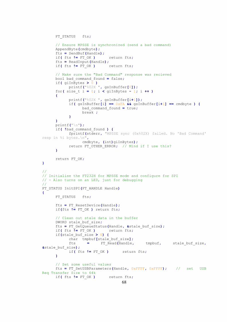
68
FT_STATUS fts; // Ensure MPSSE is synchronized (send a bad command) AppendByte(cmdbyte); fts = SendBuf(Handle); if( fts != FT_OK ) return fts; fts = ReadInput(Handle); if( fts != FT_OK ) return fts; // Make sure the "Bad Command" response was recieved bool bad_command_found = false; if( giInBytes > 0 ) printf("%02X ", gsInBuffer[0]); for( size_t i = 0; i < giInBytes - 1; i ++ ) printf("%02X ", gsInBuffer[i+1]); if( gsInBuffer[i] == 0xFA && gsInBuffer[i+1] == cmdbyte ) bad_command_found = true; break ; printf("\n"); if( !bad_command_found ) fprintf(stderr, "MPSSE sync (0x%02X) failed. No 'Bad Command' resp in %i bytes.\n", cmdbyte, (int)giInBytes); return FT_OTHER_ERROR; // Mind if I use this? return FT_OK; // // Initialise the FT232H for MPSSE mode and configure for SPI // - Also turns on an LED, just for debugging // FT_STATUS InitSPI(FT_HANDLE Handle) FT_STATUS fts; fts = FT_ResetDevice(Handle); if(fts != FT_OK ) return fts; // Clean out stale data in the buffer DWORD stale_buf_size; fts = FT_GetQueueStatus(Handle, &stale_buf_size); if( fts != FT_OK ) return fts; if(stale_buf_size > 0) char tmpbuf[stale_buf_size]; fts = FT_Read(Handle, tmpbuf, stale_buf_size, &stale_buf_size); if( fts != FT_OK ) return fts; // Set some useful values fts = FT_SetUSBParameters(Handle, 0xFFFF, 0xFFFF); // set USB Req Transfer Size to 64k if( fts != FT_OK ) return fts;

69
fts = FT_SetChars(Handle, false, 0, false, 0); // Disable event/error chars if( fts != FT_OK ) return fts; fts = FT_SetTimeouts(Handle, 3000, 3000); // set read/write timeouts to 3s if( fts != FT_OK ) return fts; fts = FT_SetLatencyTimer(Handle, 1); // Set latency timer to 1ms (default is 16ms) if( fts != FT_OK ) return fts; fts = FT_SetFlowControl(Handle, FT_FLOW_RTS_CTS, 0x00, 0x00); //Turn on flow control to synchronize IN requests (added by Andrew) if( fts != FT_OK ) return fts; fts = FT_SetBitMode(Handle, 0, 0x00); // Reset. if( fts != FT_OK ) return fts; Sleep(50); // quick nap fts = FT_SetBitMode(Handle, 0, 0x02); // Enable MPSSE mode if( fts != FT_OK ) return fts; // Sleep for a bit for USB to catch up Sleep(50); // Sync (send 0xAA - bad command) fts = InitSPI_BadCmd(Handle, 0xAA); if( fts != FT_OK ) return fts; // Second sync (0xAB) fts = InitSPI_BadCmd(Handle, 0xAB); if( fts != FT_OK ) return fts; // Base clock is 60MHz // Caution: high and low periods must be longer than 2 CPU clock cycles uint16_t divisor = 1200; // 50KHz //uint16_t divisor = 60; // 1MHz (cannot run at this speed with a 2MHz system clock) AppendByte(0x8A); // Disable clock front stage divisor (/5) AppendByte(0x97); // Disable adaptive clocking AppendByte(0x8D); // Disable 3-phase data clock SendBuf(Handle); AppendByte(0x80); // "Set Data Bits Low Byte" AppendByte(0x00); AppendByte(0x0B); // NOTE: The below is for the debug LED AppendByte(0x82); // "Set Data Bits High Byte (AC Bus)" AppendByte(0x01); // (ACBUS0 High - Status LED) AppendByte(0x01); // Clock divisor AppendByte(0x86); AppendByte((divisor/2-1) & 0xFF); // Low AppendByte((divisor/2-1) >> 8 ); // High SendBuf(Handle); // Wait a bit to ensure the chip is ready Sleep(30); // Turn off loopback on TDI/TDO connection AppendByte(0x85); SendBuf(Handle); // All done!

70
return FT_OK; // // Raise the CS line // FT_STATUS SPI_CSRaise(FT_HANDLE Handle) // 5 repeats for 1us // - each command takes 0.2us to perform, so ensures that the // line is high for at least 1us before data is sent for( int i = 0; i < 5; i ++ ) AppendByte(0x80); // GPIO ADBUS AppendByte(0x08); // CS line High AppendByte(0x0B); // (output mode, shouldn't change) return FT_OK; // Lower the CS line FT_STATUS SPI_CSLower(FT_HANDLE Handle) // - 5 repeats for 1us (each command aparently raises for 0.2us)? for( int i = 0; i < 5; i ++ ) AppendByte(0x80); // GPIO ADBUS AppendByte(0x00); // CS line low AppendByte(0x0B); // (output mode, shoudn't change) return FT_OK; // // Write a sequence of bytes to the SPI bus // FT_STATUS SPIWriteBytes(FT_HANDLE Handle, size_t Len, const void *Data) const uint8_t *bdata = Data; if( Len == 0 ) return FT_OK; // 0 = 1 byte, 0xFFFF = 2^16 bytes // - So, subtract one Len -= 1; // NOTE: CS is active-low SPI_CSLower(Handle); AppendByte(0x11); // MSB Falling Edge Change Clock - out on -ve clock edge AppendByte(Len & 0xFF); // LSB AppendByte(Len >> 8); // MSB // Append data from input buffer for( size_t i = 0; i < Len+1; i ++ ) AppendByte(bdata[i]); SPI_CSRaise(Handle);

71
return SendBuf(Handle); int main(int argc, char *argv[]) FT_STATUS fts; // Check for correct usage if( argc != 2 ) fprintf(stderr, "Usage: %s ID\n", argv[0]); DWORD ndev; fts = FT_CreateDeviceInfoList(&ndev); if( fts != FT_OK ) fprintf(stderr, "Enum failed, FT_CreateDeviceInfoList, fts = %i\n", fts); return 1; printf("%i devices\n", ndev); return -1; // Open the device int port = atoi(argv[1]); fts = FT_Open(port, &gDeviceHandle); if( fts != FT_OK ) fprintf(stderr, "FT_Open(%i) failed, fts = %i\n", port, fts); return 1; // Initialise SPI fts = InitSPI(gDeviceHandle); if( fts != FT_OK ) fprintf(stderr, "InitSPI failed, fts = %i\n", fts); return 1; // Continuously send test data to the device while( 1 ) uint8_t data[] = 0x37; fts = SPIWriteBytes(gDeviceHandle, sizeof(data), data); sleep(10); // Clean up, like a good program FT_Close(gDeviceHandle); return 0;

72
Appedix C SPI cfigurati
Appedix C1 SPI des
Fr the fwig tabe
• CP0 eas the base vaue f the cc is er
• CP1 eas the base vaue f the cc i e
• CPHA0 eas sape the eadig (first) cc edge
• CPHA1 eas sape the traiig (secd) cc edge
de CP CPHA
0 0 0
1 0 1
2 1 0
3 1 1

73
Appedix C2 SPI Settigs t Cuicate with FT232H
Settig Vaue
Cc frequecy 50H This ca be icreased as g as the high
ad w ties are ger tha tw f the
icrctrer cc perids
Ediaess st sigificat bit first
Cc parity (CP) 0
Cc phase (CPHA) 0
Chip seect parity w eabe
FT232H trasissi directi Currety set t write y with pcde 0x11
Ca be set t bidirecti with pcde 0x34

74
8 Refereces
AA Prtabe Pwer Crp 2012 iH Battery Pac 7.2V 4500Ah fr RC10 Cars ad Su Rbts Avaiabe fr httpwwwbatteryspacecihbatterypac72v4500ahfrrc10carsadsurbtsaspx> accessed 5 uy 2012
Ate Crprati 2009 AVR1005 Gettig started with XEGA Avaiabe fr wwwatecIagesdc8169pdf> accessed 24 ctber 2012
Ate Crprati 2009 xega A aua Avaiabe fr wwwatecIagesdc8077pdf> accessed 18 uy 2012
Ate Crprati 2012 AVR1300 Usig the Ate AVR XEGA ADC Avaiabe fr httpwwwatecIagesdc8032pdf> accessed 2 veber 2012
Ate Crprati d AVR Drag PDI Prgraig Avaiabe fr httpwwwatewebdcavrdragavrdragpdidescriptiht> accessed 30 ctber 2012
Baiey DG 2011 Desig fr Ebedded Iage Prcessig FPGAs h Wiey & Ss
BeageBardrg BeageBard Hardware Desig Avaiabe fr httpbeagebardrghardwaredesig> accessed 20 arch 2012
Bacha B 2006 The Devepet f a Hardware Patfr fr Reatie Iage Prcessig Hurs thesis Uiversity f Wester Austraia
Bru T EyeBt ie Dcuetati The Uiversity f Wester Austraia Avaiabe fr httprbticseeuwaeduaueyebt> accessed 30 arch 2012
Bru T 2012 EEC2303 ab aua The Uiversity f Wester Austraia
Chi 2006 FPGA Based Ebedded Visi Systes Hurs thesis Uiversity f Wester Austraia
Cey G 2010 BeageBardx Rev C Syste Referece aua C10 vs BeageBardrg

75
Dietrich B 2009 Desig ad Ipeetati f a FPGAbased Stere Visi Syste fr the EyeBt 6 asters thesis Techische Uiversitt che ad The Uiversity f Wester Austraia
Du 2003 Swar Custerig Syste with ca Iage Prcessig ad Cuicati asters thesis Uiversity f Wester Austraia ad Uiversity f Stuttgart
Ewa aced 2008 Eyebt 6 Ctred Sesr Pacage i a Reewabe Eergy Vehice Hyudai Get The Uiversity f Wester Austraia
Future Techgy Devices Iteratia td 2011 Appicati te A108 Cad Prcessr fr PSSE ad CU Hst Bus Euati des Avaiabe fr httpwwwftdichipcDcuetsApptesA108CadPrcessrfrPSSEadCUHstBusEuatidespdf> accessed 8 veber 2012
Geier 2009 Desig ad Ipeetati f a FPGAbased Iage Prcessig Fraewr fr the EyeBt 6 asters thesis Techische Uiversitt che ad The Uiversity f Wester Austraia
ewis P 2008 Seay Ftprits The Quest fr a RightAge Sparfu Eectrics Avaiabe fr httpwwwsparfuctutrias114> accessed 12 August 2012
XP 2010 PCA9685 Datasheet Avaiabe fr wwwxpcdcuetsdatasheetPCA9685pdf> accessed 11 uy 2012
XP 2012 I2Cbus specificati ad user aua Avaiabe fr httpwwwxpcdcuetsuserauaU10204pdf> accessed 1 August 2012
Pu Rbtics ad Eectrics 2011 Serv ctr iterface i detai Avaiabe fr httpwwwpucbg17servctriterfaceidetai> accessed 13 August 2012
Rugged Circuits C 2011 10 Ways t Destry a Ardui Avaiabe fr httpruggedcircuitschtacp01ht> accessed 4 ctber 2012
Sigh 2011 Hardware Redesig f a Experieta Ebedded Patfr Hurs thesis Uiversity f Wester Austraia
76
Texas Istruets Icrprated 2012 2678 SIPE SWITCHER High Efficiecy 5A StepDw Vtage Reguatr (Rev. H) Avaiabe fr httpwwwticprduct2678#techicadcuets> accessed 10 ctber 2012
Texas Istruets Icrprated 2012 TS320C6000 DSP ibrary Avaiabe fr httpwwwtictsprc265> accessed 27 ay 2012
va es & Craer 2005 'Ifuecig prduct ifetie thrugh prduct desig' Busiess Strategy ad the Eviret v 14 5 pp 286299
Yaghur 2009 Buidig Ebedded iux Systes Sebastp p 232


![locQKrrSlKo ¯ S]Sc`S filesoclKc¯K¯Qo>~SK>s`c pr>`~S>_K`rcIS ´ Ksoc¯R> Gc`pK`rSrc]>loKp>S`G>oSGcIS ...](https://static.fdocumenti.com/doc/165x107/5cd49e6588c99325338d0031/locqkrrslko-sscs-kqosksc-prskrcis-ksocr-gcpkrsrclokpsgosgcis.jpg)