
CAN GMT ADC 812
38
Via dell' Artigiano, 8/6 40016 San Giorgio di Piano (Bologna) ITALY E-mail: [email protected] http://www.grifo.it http://www.grifo.com Tel. +39 051 892.052 (a. r.) FAX: +39 051 893.661 , GPC ® , grifo ® , are trade marks of grifo ® grifo ® ITALIAN TECHNOLOGY ADC 812 Rel. 5.00 Rel. 18 June 2002 CAN GMT ADC 812 Analog to Digital Converter - 8 channels 12 bit TECHNICAL MANUAL
Transcript of CAN GMT ADC 812

Via dell' Artigiano, 8/640016 San Giorgio di Piano(Bologna) ITALYE-mail: [email protected]
http://www.grifo.it http://www.grifo.comTel. +39 051 892.052 (a. r.) FAX: +39 051 893.661
, GPC®, grifo ®, are trade marks of grifo ®
grifo ®
ITALIAN TECHNOLOGY
ADC 812 Rel. 5.00 Rel. 18 June 2002
CAN GMTGeneral Purpose Controller 80c32,
80c320, 89c51Rx2
ADC 812Analog to Digital Converter - 8 channels 12 bit
TECHNICAL MANUAL
Interface for Abaco® I/O BUS on 26 pins standard low profileconnector; dimension: 100x50x30 mm, (110x60x70 mm withcontainer) in 4 type format; optional plastic support for DIN46277-1 and DIN 46277-3 Ω rails; one A/D Converter section,8 channels,12 bits, based on DAS MAX197; 9 µs conversiontime, for each channel; 5Mhz Bandwidth Track Hold , 100KspsSampling-Rate; software controlled indication of polarity ; inputrange and input channel selectable by software; available inputranges: ±10V, ±5V, +10V, +5V or 0÷20mA, 4÷20mA withoptional conversion module: .8420; fault protected inputmultiplexer (±16,5V); two 8 pins quick release screw terminalconnectors, for all analog inputs; interrupt request joined to endof conversion; interrupt connection to /INT or /NMI , selectableby hardware; only 2 consecutives Bytes used for card I/Oaddressing; card I/O allocation address defined through properdip switch; single power supply voltage: +5 Vdc; 80 mA.

DOCUMENTATION COPYRIGHT BY grifo ® , ALL RIGHTS RESERVED
No part of this document may be reproduced, transmitted, transcribed, stored in aretrieval system, or translated into any language or computer language, in any form orby any means, either electronic, mechanical, magnetic, optical, chemical, manual, orotherwise, without the prior written consent of grifo ®.
IMPORTANT
Although all the information contained herein have been carefully verified, grifo ®
assumes no responsability for errors that might appear in this document, or for damageto things or persons resulting from technical errors, omission and improper use of thismanual and of the related software and hardware.grifo ® reserves the right to change the contents and form of this document, as well as thefeatures and specification of its products at any time, without prior notice, to obtainalways the best product.For specific informations on the components mounted on the card, please refer to theData Book of the builder or second sources.
SYMBOLS DESCRIPTION
In the manual could appear the following symbols:
Attention: Generic danger
Attention: High voltage
Trade Marks
, GPC®, grifo ® : are trade marks of grifo ®.Other Product and Company names listed, are trade marks of their respective companies.
ITALIAN TECHNOLOGY grifo ®
Page I ADC 812 Rel. 5.00
GENERAL INDEXINTRODUCTION ........................................................................................................................ 1
CARD VERSION ......................................................................................................................... 1
GENERAL INFORMATIONS .................................................................................................... 2 A/D CONVERTER .................................................................................................................. 4 INPUT FILTERS ..................................................................................................................... 4 REFERENCE VOLTAGE ...................................................................................................... 6 INTERFACING AND ADDRESSING................................................................................... 6
TECHNICAL FEATURES .......................................................................................................... 7 GENERAL FEATURES..........................................................................................................7 PHYSICAL FEATURES.........................................................................................................7 ELECTRIC FEATURES ........................................................................................................ 7
INSTALLATION .......................................................................................................................... 8 TRIMMERS AND CALIBRATION ...................................................................................... 8 TEST POINT ........................................................................................................................... 8 CONNECTIONS ................................................................................................................... 10 CN2 - A/D CONVERTER INPUTS 0÷3 CONNECTOR .............................................. 10 CN3 - A/D CONVERTER INPUTS 4÷7 CONNECTOR .............................................. 12 CN1 - ABACO® I/O BUS CONNECTOR....................................................................... 13 I/O CONNECTION ............................................................................................................... 14 TYPE OF ANALOG INPUT SELECTION ........................................................................ 14 JUMPERS .............................................................................................................................. 15 POWER SUPPLY SELECTION.......................................................................................... 15 MECHANICAL MOUNTING ............................................................................................. 16 INTERRUPT.......................................................................................................................... 16
ADDRESSES AND MAPS ......................................................................................................... 17 BOARD MAPPING............................................................................................................... 17 I/O ADDRESSES ................................................................................................................... 18
PERIPHERAL DEVICES SOFTWARE DESCRIPTION ..................................................... 19 A/D CONVERTER ................................................................................................................ 19 INITIALIZATION SEQUENCE .................................................................................... 22 POLLING CONVERSION.............................................................................................. 22 INTERRUPT CONVERSION......................................................................................... 22
EXTERNAL CARDS .................................................................................................................23
BIBLIOGRAPHY....................................................................................................................... 27
APPENDIX A: ALPHABETICAL INDEX ............................................................................ A-1

grifo ® ITALIAN TECHNOLOGY
Page II ADC 812 Rel. 5.00
FIGURES INDEXFIGURE 1: CARD PHOTO ................................................................................................................... 3FIGURE 2: COMPONENTS MAP ........................................................................................................... 3FIGURE 3: BLOCK DIAGRAM ............................................................................................................. 5FIGURE 4: TEST POINT FOR REFERENCE VOLTAGE .............................................................................. 8FIGURE 5: CONNECTORS, TEST POINT, DIP SWITCH, ETC. LOCATION .................................................... 9FIGURE 6: A/D CONVERTER INPUTS 0÷3 CONNECTOR ...................................................................... 10FIGURE 7: ANALOG INPUT BLOCK DIAGRAM .................................................................................... 11FIGURE 8: A/D CONVERTER INPUTS 0÷3 CONNECTOR ...................................................................... 12FIGURE 9: CN1 - ABACO® I/O BUS CONNECTOR ....................................................................... 13FIGURE 10: JUMPER SUMMARIZING TABLE ....................................................................................... 15FIGURE 11: INTERNAL REGISTERS ADDRESSES TABLE ........................................................................ 18FIGURE 12: POSSIBLE CONNECTIONS DIAGRAM ................................................................................ 25

ITALIAN TECHNOLOGY grifo ®
Page 1 ADC 812 Rel. 5.00
INTRODUCTIONINTRODUCTION
The use of these devices has turned - IN EXCLUSIVE WAY - to specialized personnel.
The purpose of this handbook is to give the necessary information to the cognizant and sure use ofthe products. They are the result of a continual and systematic elaboration of data and technical testssaved and validated from the manufacturer, related to the inside modes of certainty and quality ofthe information.
The reported data are destined- IN EXCLUSIVE WAY- to specialized users, that can interact withthe devices in safety conditions for the persons, for the machine and for the enviroment, impersonatingan elementary diagnostic of breakdowns and of malfunction conditions by performing simplefunctional verify operations , in the height respect of the actual safety and health norms.
The informations for the installation, the assemblage, the dismantlement, the handling, the adjustment,the reparation and the contingent accessories, devices etc. installation are destined - and thenexecutable - always and in exclusive way from specialized warned and educated personnel, ordirectly from the TECHNICAL AUTHORIZED ASSISTANCE, in the height respect of themanufacturer recommendations and the actual safety and health norms.
The devices can't be used outside a box. The user must always insert the cards in a container thatrispect the actual safety normative. The protection of this container is not threshold to the onlyatmospheric agents, but specially to mechanic, electric, magnetic, etc. ones.
To be on good terms with the products, is necessary guarantee legibility and conservation of themanual, also for future references. In case of deterioration or more easily for technical updates,consult the AUTHORIZED TECHNICAL ASSISTANCE directly.
To prevent problems during card utilization, it is a good practice to read carefully all the informationsof this manual. After this reading, the user can use the general index and the alphabetical index,respectly at the begining and at the end of the manual, to find information in a faster and more easyway.
CARD VERSIONCARD VERSION
The present handbook is reported to the ADC 812 card release 240398 and later. The validity of thebring informations is subordinate to the number of the card release. The user must always verify thecorrect correspondence among the two denotations. On the card the release number is present in morepoints both board printed diagram (serigraph) and printed circuit (for example near capacitor C16both on the component sideand on the solder side).
grifo ® ITALIAN TECHNOLOGY
Page 2 ADC 812 Rel. 5.00
GENERAL INFORMATIONSGENERAL INFORMATIONS
The ADC 812 is a powerfull peripheral, high speed, low price, analog to digital converter card,included in Abaco® industrial family. It is composed by a 12 bits A/D converter section, based onthe multi range MAX197 DAS (Data Acquisition System) and it provides 8 indipendent analoginputs.The electric connection of the card is performed through three confortable connectors: one for thecontrol cards with Abaco® I/O BUS, and the other two for the input analog signals; the mechanicalmounting is simplified by a proper optional plastic support for DIN 46277-1 and DIN 46277-3omega rails.The ADC 812 card is the right component for all the applications where it is required a low price,an high number of signals to be acquired and an high conversion speed. If the number of requiredanalog input channels is higher than those available on the board, it is moresuitable an europe cardsize with Abaco® BUS.A very important feature of ADC 812 are the multi range analog inputs, in fact with a simplesoftware setting, many different input signals can be converted; furthermore, there are two handysockets 8 way each, where you can mount up to 8 precision resistors to quickly specialize, each oneof the eight voltage inputs, into current inputs in the range 0÷20mA or 4÷20mA.A wide range of demo programs and examples allow an immediate use of the same. These programsare available for the whole CPUs of Abaco® family. They are duly documented and supplied undersource form for many different languages in which Abaco® control cards can be programmed.
- Interface for Abaco® I/O BUS on 26 pins standard low profile connector.- Dimension: 100x50x40 mm, (110x60x70 mm with container) in 4 type format.- Optional plastic support for DIN 46277-1 and DIN 46277-3 Ω rails.- One A/D Converter section, 8 channels,12 bits, based on DAS MAX197.- 9 µs conversion time, for each channel.- 5Mhz Bandwidth Track Hold , 100Ksps Sampling-Rate.- Software controlled indication of polarity .- Input range and input channel selectable by software.- Available input ranges: ±10V, ±5V, +10V, +5V or 0÷20mA, 4÷20mA with optional conversion
module: .8420.- Fault protected input multiplexer (±16.5V)- Two 8 pins quick release screw terminal connectors, for all analog inputs.- Interrupt request joined to end of conversion.- Interrupt connection to /INT or /NMI , selectable by hardware.- Only 2 consecutives Bytes used for card I/O addressing.- Card I/O allocation address defined through proper dip switch.- Single power supply voltage: +5 Vdc; 80 mA.
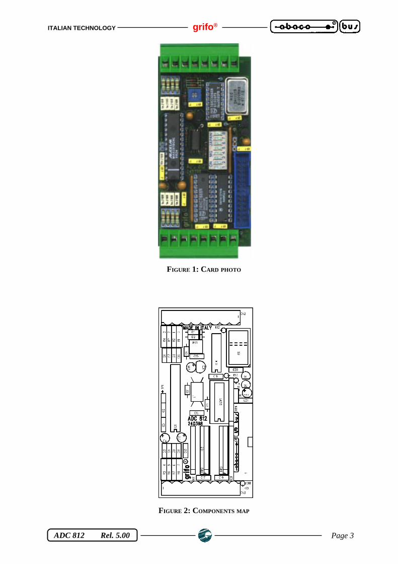
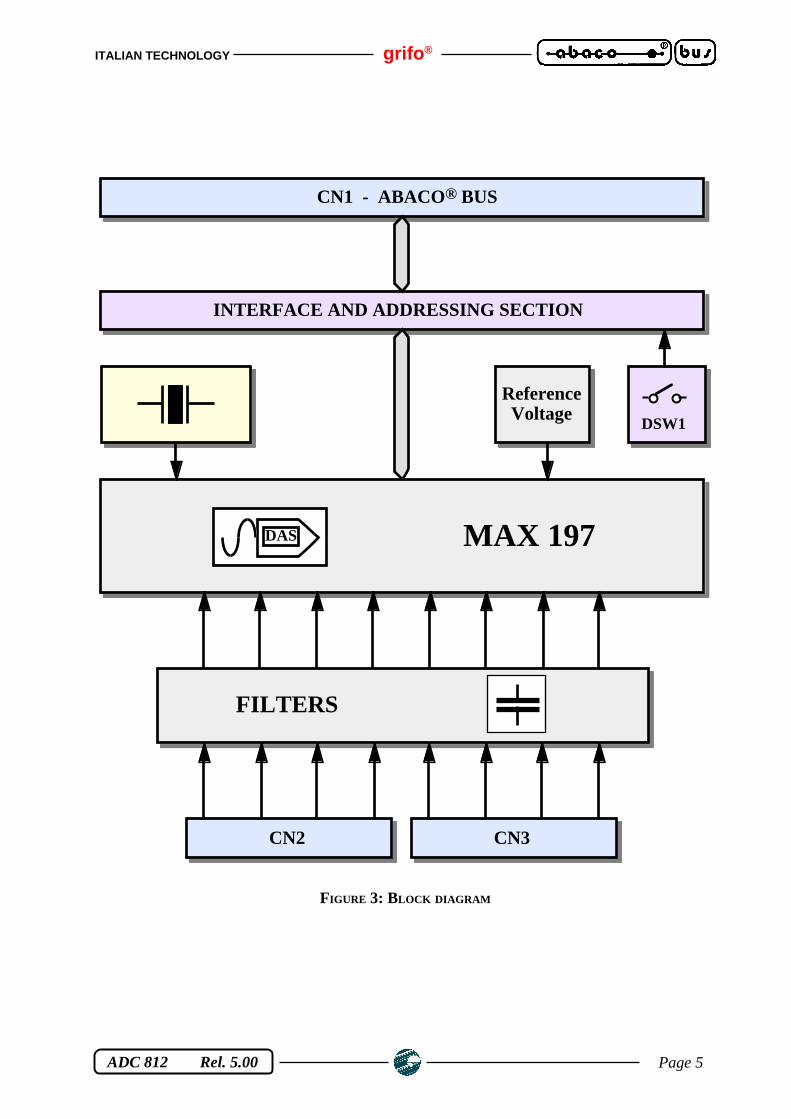
Here follows a description of the board's functional blocks, with an indication of the operationsperformed by each one. To easily locate these blocks and verify their connections pleare refer tofigure 3.
ITALIAN TECHNOLOGY grifo ®
Page 3 ADC 812 Rel. 5.00
FIGURE 1: CARD PHOTO
FIGURE 2: COMPONENTS MAP
grifo ® ITALIAN TECHNOLOGY
Page 4 ADC 812 Rel. 5.00
A/D CONVERTER
DAC 812 performs the eight channels A/D conversion by a MAX 197, that is a multi-range, 12-bitdata-acquisition system (DAS) which uses successive approximation and internal track/holdcircuitry.Main features of this device are:
- Resolution 12 bits in unipolar mode or 11 bits plus sign in bipolar mode.- Multi-range software configurable inputs, allowed ranges are 0÷5 V, 0÷10 V, ±5 V, ±10 V.- Conversion time per channel 6 µsec.- Maximum linearity error ±1 LSB.- Fault Protected Input Multiplexer (±16.5 V).- 5 MHz Bandwitdh Track Hold, sample rate per channel 100 Ksps indipendent for each section.- easy software management; end-of-conversion interrupt generation.
MAX 917 is the ideal component for common applications in industrial automation, where bothconversion speed and resolution must be high. For further information please refer to manufacturersinformation.
INPUT FILTERS
The eigth analog inputs of ADC 812 are provided with a filtering circuitery that decrease sensibilityto field noises. These sections are based on high precision components and are set up in laboratory,to deliver cards with the same interfacement.The filters are made to install an optional module for current-to-voltage conversion which is basedon 248 Ω selected precision resistors that allow to acquire signals in the range 0÷20 mA or 4÷20 mA.For further information please refer to figure 7.
ITALIAN TECHNOLOGY grifo ®
Page 5 ADC 812 Rel. 5.00
FIGURE 3: BLOCK DIAGRAM
INTERFACE AND ADDRESSING SECTION
CN1 - ABACO® BUS
CN3
DSW1
CN2
DAS MAX 197
FILTERS
ReferenceVoltage
grifo ® ITALIAN TECHNOLOGY
Page 6 ADC 812 Rel. 5.00
REFERENCE VOLTAGE
A precision circuitery is charged to generate the reference voltage required by the A/D convertersection. This circuitery is designed to provide a tension stabilized and indipendent from ADC 812on board power supply and temperature changes, obtaining a greater precision.This tension is calibrated in test phase and the user must not change it. For further information pleaserefer to paragraph “TRIMMER ADN CALIBRATIONS”.
INTERFACING AND ADDRESSING
This section manages the data exchange between CAN controller and command board; in particular,all written or read data transit across this section that, in addition, provides the board I/O managementin its addressing space and an eventual interrupt generation by setting the dip switch DSW1.Physical connection to command boards is performed through ABACO® I/O BUS, featuring 8 databits, but it can be extended to ABACO® BUS using specific conversion modules like ABB 05 or ABB03.Interfacing and addressing section is based on logic gates and buffers carefully selected to warranta correct working under any condition and minimize the room taken.
ITALIAN TECHNOLOGY grifo ®
Page 7 ADC 812 Rel. 5.00
TECHNICAL FEATURESTECHNICAL FEATURES
GENERAL FEATURES
BUS: ABACO® I/O BUSAnalog signals: 8Addressing space: 256 bytesBytes taken: 2
On board resources: DAS MAX 197Oscillator frequency: 8 MHzWork frequency: 2 MHzConversion time: 9 µsec per channelA/D Resolution: 12 bit (Unipolar mode)
11 bit + sign (Bipolar mode)Linearity maximum error: ±1 LSB (*)Offset maximum error: ±1 LSB (*)Diffrential input error: ±1 LSB (*)
Connectors: CN1: 26 pins low profile vertical maleCN2: 8 pins quick release screw terminalCN3: 8 pins quick release screw terminal
PHYSICAL FEATURES
Size: 100 x 50 x 30 mm (without container)110 x 60 x 65 mm (with DIN container)
Weight: 85 g
Temperature range: 0÷50 °C
Relative humidity: 20%÷90% (without condense)
ELECTRIC FEATURES
Power supply voltage: +5 Vdc
Consumption on +5 Vdc: 80 mA
Input impedance: 21 kΩ (unipolar mode)16 kΩ (bipolar mode)
Cut off frequency: 1 MHz
* Data here reported are referred to a 20 centigrad degreeeses environmental temperature
grifo ® ITALIAN TECHNOLOGY
Page 8 ADC 812 Rel. 5.00
INSTALLATIONINSTALLATION
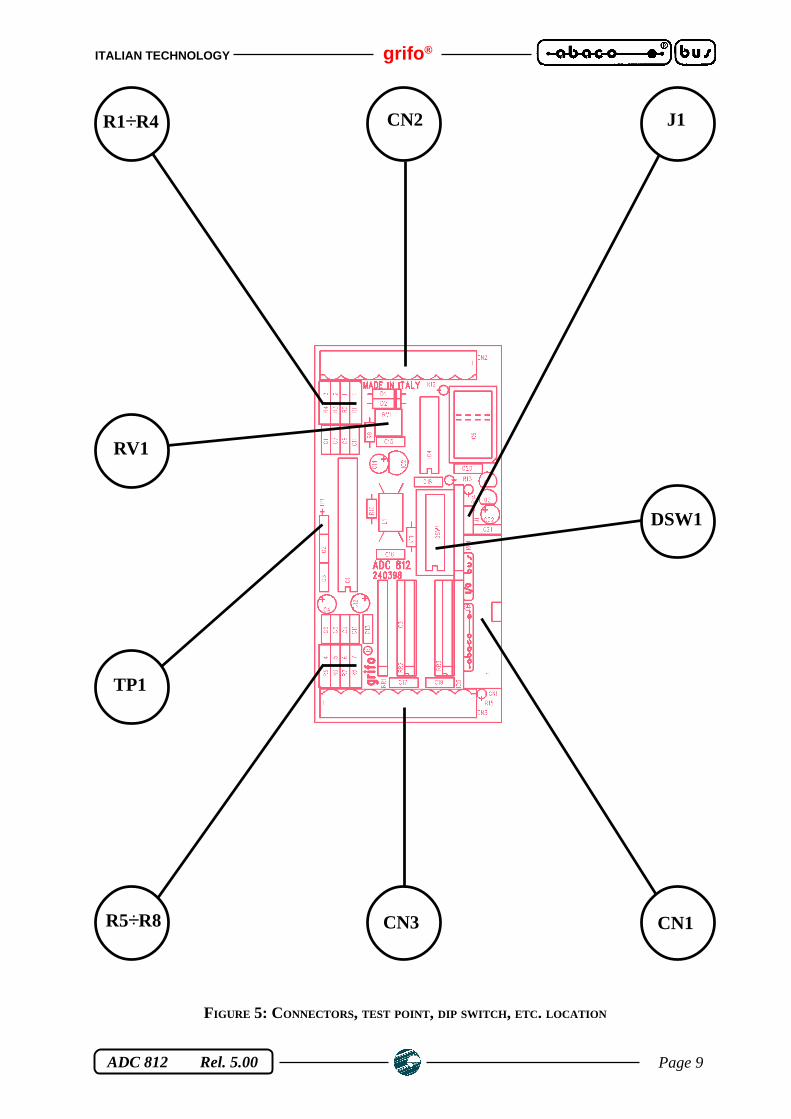
In this chapter there are the information for a right installation and correct use of the card. The usercan find the location and functions of each connectors, dip switch, LEDs, etc. and some explanatorydiagrams.
TRIMMER AND CALIBRATION
On ADC 812 there is available a trimmer, named RV1, that calibrates the Vref voltage of the optionalA/D converter section. The ADC 812 is subjected to a careful test that verifies and calibrates all thecard sections. To easily locate the trimmer, please refer to figure 5. The calibration is executed inlaboratory, with a conntrolled +20 C° room temperature, following these steps:
-The A/D voltage reference (Vref) is calibrated through RV1 trimmer, by using a 5 digits precisionmultimeter, to a value of +4,096 Vdc, measured on test point TP1.
- The corrispondance between the analog input signal and the combination read from A/D is verified.This check is performed with a reference signal connected to A/D inputs and testing that the A/Dcombination and the theoric combination differ at maximum of the A/D section errors sum.
- The trimmer is blocked with paint.
The analog interfaces use high precision components that are selected during mounting phase toavoid complicate and long calibration procedures. After the calibration, the on board trimmer isblocked with paint to mantain calibration also in presence of mechanic stresses (vibrations, movings,delivery, etc.).The user must not modify the card calibration, but if thermic drifts,time drifts and so on, makenecessary a new calibration, the user must strictly follow the previous described procedure.
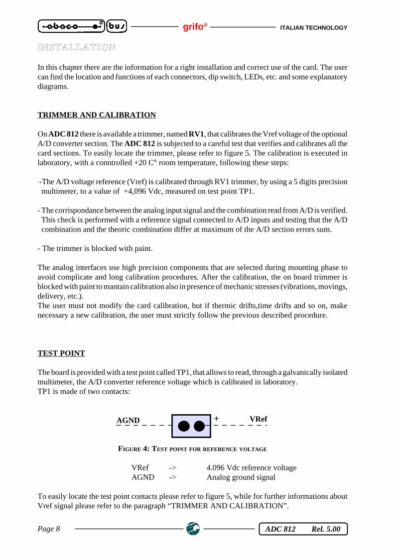
TEST POINT
The board is provided with a test point called TP1, that allows to read, through a galvanically isolatedmultimeter, the A/D converter reference voltage which is calibrated in laboratory.TP1 is made of two contacts:
FIGURE 4: TEST POINT FOR REFERENCE VOLTAGE
VRef -> 4.096 Vdc reference voltageAGND -> Analog ground signal
To easily locate the test point contacts please refer to figure 5, while for further informations aboutVref signal please refer to the paragraph “TRIMMER AND CALIBRATION”.
AGND VRef+
ITALIAN TECHNOLOGY grifo ®
Page 9 ADC 812 Rel. 5.00
FIGURE 5: CONNECTORS, TEST POINT, DIP SWITCH , ETC. LOCATION
DSW1
R1÷R4
R5÷R8 CN1
TP1
CN3
RV1
J1CN2
grifo ® ITALIAN TECHNOLOGY
Page 10 ADC 812 Rel. 5.00
CONNECTIONS
The ADC 812 module has 3 connectors that can be linkeded to other devices or directly to the field,according to system requirements. In this paragraph there are connectors pin out, a short signalsdescription (including the signals direction), connectors location (please refer to figure 5) and someelectrical diagrams that shows the on board circuit of each connector.
CN2 - A/D CONVERTER INPUTS 0÷3 CONNECTOR
CN2 is a 8 pins, quick release screw terminal connector.Through CN2 the first 4 A/D converter section input signals interface to the external world, in detailinputs from 0 to 3 of A/D converter section are available.Analog lines are provided with a low-pass filter and are placed in order to reduce interference andelectricale nois warranting a good signal transmission and in order to simplify connection with othersystems.
FIGURE 6: A/D CONVERTER INPUTS 0÷3 CONNECTOR
Signals description:
CHn+ = I - n-th analog input.CHn- = I - n-th analog input ground.
CH3 +
CH3 -
CH2 +
CH2 -
CH1 +
CH0 +
CH0 -
CH1 -
8
7
5
4
2
1
3
6
ITALIAN TECHNOLOGY grifo ®
Page 11 ADC 812 Rel. 5.00
FIGURE 7: ANALOG INPUT BLOCK DIAGRAM
VRef.
CN
3
DA
S M
AX
197
23
22
21
20
19
18
17
16
AN. GND
15
2
4
6
8
2
6
8
4
1, 3, 5, 7
CN
2
1, 3, 5, 7
R1
R2
R3
R4
R5
R6
R7
R8
VR1

grifo ® ITALIAN TECHNOLOGY
Page 12 ADC 812 Rel. 5.00
CN3 - A/D CONVERTER INPUTS 4÷7 CONNECTOR
CN3 is a 8 pins, quick release screw terminal connector.Through CN3 the second 4 A/D converter section input signals interface to the external world, indetail inputs from 4 to 7 of A/D converter section are available.Analog lines are provided with a low-pass filter and are placed in order to reduce interference andelectricale nois warranting a good signal transmission and in order to simplify connection with othersystems.
FIGURE 8: A/D CONVERTER INPUTS 0÷3 CONNECTOR
Signals description:
CHn+ = I - n-th analog input.CHn- = I - n-th analog input ground.
1
2
3
4
5
7
8
6
CH4 -
CH4 +
CH5 -
CH5 +
CH6 -
CH7 -
CH7 +
CH6 +

ITALIAN TECHNOLOGY grifo ®
Page 13 ADC 812 Rel. 5.00
CN1 - ABACO® I/O BUS CONNECTOR
CN1 is a 26 pins, male, vertical, low profile connector with 2.54 mm pitch.Through CN1 the card can be connected via ABACO® I/O BUS to some of the numerous grifo ®
boards,both intelligent and not. For example the user can directly use cards for analog signalsacquisition (A/D), cards for analog signals generation (D/A), cards for digital I/O signals management,cards with timers and counters, etc. All this connector signals are at TTL level.
FIGURE 9: CN1 - ABACO® I/O BUS CONNECTOR
Signals description:A0÷A7 = O - Address BUS.D0÷D7 = I/O - Data BUS./INT BUS = I - Interrupt request (open collector type)./NMIBUS = I - Non mascable interrupt./IORQ = O - Input output request./RD = O - Read cycle status./WR = O - Write cycle status./RESET = O - Reset.+5 Vdc = I - +5 Vdc power supply.GND = - Ground signal.N.C. = - Not connected.
1 2
3 4
5 6
7 8
9 10
11 12
13 14
D0
D2
D4
D6
A0
A2
A4
D1
D3
D5
D7
A1
A3
A5
15 16
17 18
19 20
A6
/WR
/IORQ
A7
/RD
/INT BUS
21 22
23 24
25 26
N.C.
GND
N.C.
+5 Vdc
N.C.
/NMI BUS
grifo ® ITALIAN TECHNOLOGY
Page 14 ADC 812 Rel. 5.00
I/O CONNECTION
To prevent possible connecting problems between GPC® 153 and the external systems, the user hasto read carefully the information of the previous paragraphs and he must follow these instrunctions:
- For all TTL signals the user must follow the rules of this electric standard. The connected digitalsignal must be always referred to card digital ground (GND). For TTL signals, the 0 Vdc levelcorresponds to logic state "0", while 5Vdc level corrisponds to logic state "1". For ABACO® I/OBUS signals it is suggsted to use connection of at most 10 centimeters.
- The analog inputs (A/D section) must be connected to low impedance signals in the selected voltagerange (please refer to paragraph“SOFTWARE DESCRIPTION”). Remember that the eight analoginputs available on CN2 and CN3 are provided of filter capacitors that ensure an higher stabilityof the acquired signals, but reduce at the same time the bandwith frequency.
TYPE OF ANALOG INPUT SELECTION
ADC 812 board can accept analog voltage and/or current inputs, as described in the previousparagraphs and chapters. The input type selection must be made during the order phase and isperformed mounting a specific voltage-current conversion module (option code .8420) made byprecision resistors. In detail:
R1 -> channel 0R2 -> channel 1R3 -> channel 2R4 -> channel 3R5 -> channel 4R6 -> channel 5R7 -> channel 6R8 -> channel 7
Should the voltage-current conversion module not to be mounted (default case) the correspondingchannel accepts a voltage input signal in the ranges 0÷5 V, 0÷10 V, ±5 V or ±10 V; otherwise a currentinput signal is accepted.In this latter case the input range must be set as 0÷5 V, so the value of the above mentioned resistorsis obtained by the following spread;
R = 5 V / Imax
Usually the voltage-current conversion modules are made using 248 Ω precision resistors,corresponding to 4÷20 mA or 0÷20 mA.Any eventual configuration out of this standard shold be asked directly to grifo ®.To easily locate the voltage-current conversion module please refer to figure 5.
ITALIAN TECHNOLOGY grifo ®
Page 15 ADC 812 Rel. 5.00
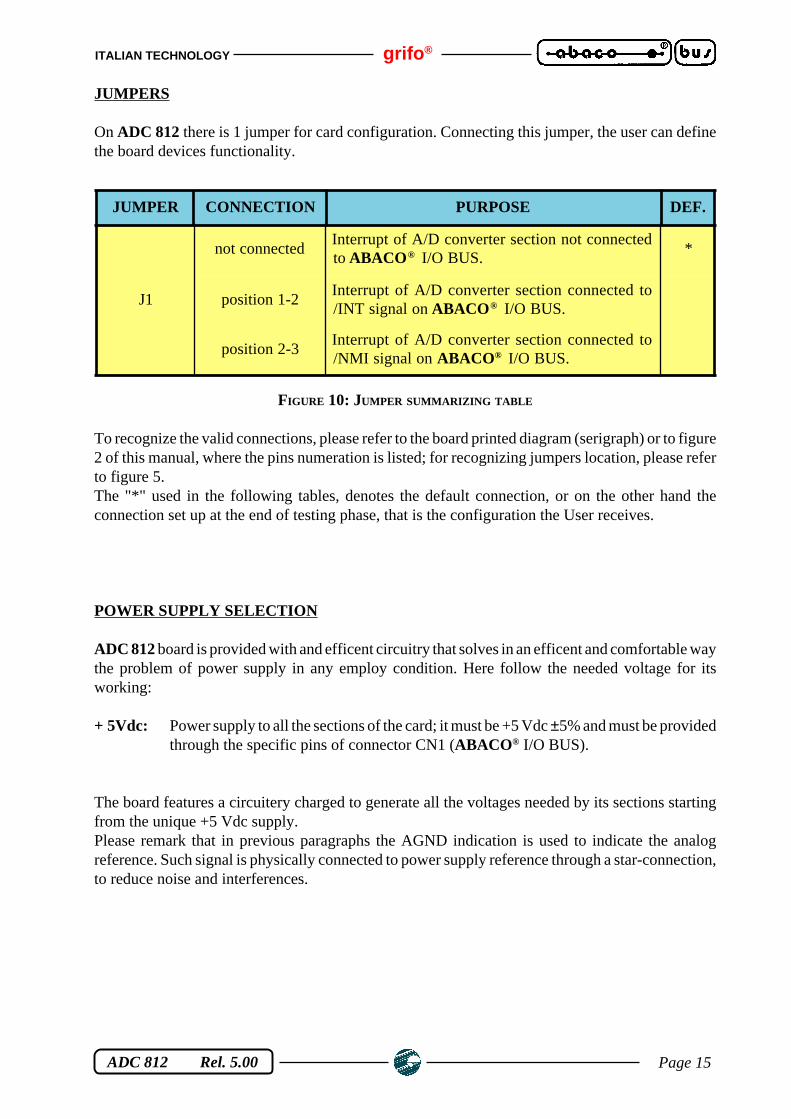
JUMPERS
On ADC 812 there is 1 jumper for card configuration. Connecting this jumper, the user can definethe board devices functionality.
FIGURE 10: JUMPER SUMMARIZING TABLE
To recognize the valid connections, please refer to the board printed diagram (serigraph) or to figure2 of this manual, where the pins numeration is listed; for recognizing jumpers location, please referto figure 5.The "*" used in the following tables, denotes the default connection, or on the other hand theconnection set up at the end of testing phase, that is the configuration the User receives.
POWER SUPPLY SELECTION
ADC 812 board is provided with and efficent circuitry that solves in an efficent and comfortable waythe problem of power supply in any employ condition. Here follow the needed voltage for itsworking:
+ 5Vdc: Power supply to all the sections of the card; it must be +5 Vdc ±5% and must be providedthrough the specific pins of connector CN1 (ABACO® I/O BUS).
The board features a circuitery charged to generate all the voltages needed by its sections startingfrom the unique +5 Vdc supply.Please remark that in previous paragraphs the AGND indication is used to indicate the analogreference. Such signal is physically connected to power supply reference through a star-connection,to reduce noise and interferences.
JUMPER CONNECTION PURPOSE DEF.
J1
not connectedInterrupt of A/D converter section not connectedto ABACO ® I/O BUS.
*
position 1-2Interrupt of A/D converter section connected to/INT signal onABACO ® I/O BUS.
position 2-3Interrupt of A/D converter section connected to/NMI signal onABACO® I/O BUS.
grifo ® ITALIAN TECHNOLOGY
Page 16 ADC 812 Rel. 5.00
MECHANICAL MOUNTING
By default, ADC 812 board is provided without any container, but optionally are available items thateasy remarkably its mechanical mounting. These items are plastic container designed to be installedon Ω rails type DIN 46277-1 and DIN 46277-3, like, for example, item BLOCK.100.50. Should theADC 812 be matched to other boards provided with ABACO® I/O BUS, it is possible to order anunique container for all the boards, to simplify the mounting and reduce the costs. For furtherinformation please call grifo ® directly.
INTERRUPT
ADC 812 is provided with a comfortable and efficent interrupt generation circuitery, that, if enabled,can generate an interrupt to the GPC® control card when conversion ends. Such circuitery allows tooptimize the time needed to manage the board, in fact the GPC® intelligent control card is not obligedto poll ADC 812 registers, but can simply wait for an interrupt and manage the new data interchange.ABACO® I/O BUS interrupt signal remains activated until the control card accesses ADC 812 to readthe conversion value. This warrants a correct management also in case of multiple interrupt becausethe interrupt is disengaged only by an appropriate software management, which is time independent.Please remark that interrupt generation circuitery can be connected or not connected to ABACO®
I/O BUS through the specific jumper J1 as described in the paragraph “JUMPER”.

ITALIAN TECHNOLOGY grifo ®
Page 17 ADC 812 Rel. 5.00
ADDRESSES AND MAPSADDRESSES AND MAPS
In this chapter are reported all information about card use, related to hardware and software. Forexample, the registers addresses and the memory allocation are described below.
BOARD MAPPING
ADC 812 board is mapped into a 2 bytes I/O addressing space, that can be allocated starting fromdifferent base addresses according to how the board is configured. This feature allows to use severalAD C 812 cards on the same ABACO® I/O BUS or ABACO® BUS, or to install them on a BUS whereother peripheral modules are installed obtaining a structure that can be expanded without anydifficulty or modifications to the application software. These bytes allow the complete control ofboard settings and status and the complete flow of input and output data.The base address can be defined through the specific BUS interface circuitry on the board itself; thiscircuitry uses the eight pins dip switch called DSW1, from which it reads the address set by the user.Here follows the corrispondance between dips configuration and address signals, to easily locatesuch component please refer to figure 5.
DSW1.1 -> Not usedDSW1.2 -> Bit A1DSW1.3 -> Bit A2DSW1.4 -> Bit A3DSW1.5 -> Bit A4DSW1.6 -> Bit A5DSW1.7 -> Bit A6DSW1.8 -> Bit A7
These dips are driven in complemented logic, this means that if a switch is ON generates a logiczero, viceversa if a switch is OFF generates a logic one.
NOTEWhen allocating the mapping address of the boards, plase be careful not to allocate more than onedevice in the same addressing space (count also the number of bytes occupied by the card). If thiscondtion will not be respected, a BUS conflict will happen; such conflict will compromise the correctworking of the whole system.
As an example, dip configuration to set address 048H is repored here:
DSW1.1 -> IndifferentDSW1.2 -> ONDSW1.3 -> ONDSW1.4 -> OFFDSW1.5 -> ONDSW1.6 -> ONDSW1.7 -> OFFDSW1.8 -> ON
grifo ® ITALIAN TECHNOLOGY
Page 18 ADC 812 Rel. 5.00
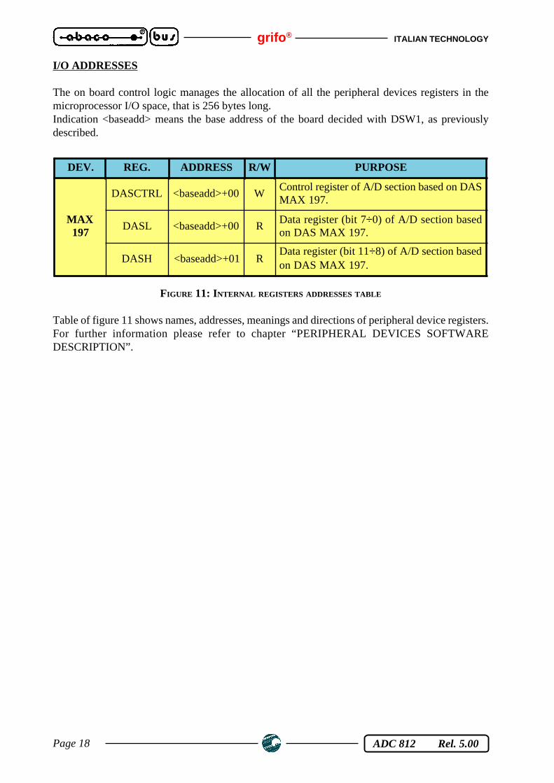
I/O ADDRESSES
The on board control logic manages the allocation of all the peripheral devices registers in themicroprocessor I/O space, that is 256 bytes long.Indication <baseadd> means the base address of the board decided with DSW1, as previouslydescribed.
FIGURE 11: INTERNAL REGISTERS ADDRESSES TABLE
Table of figure 11 shows names, addresses, meanings and directions of peripheral device registers.For further information please refer to chapter “PERIPHERAL DEVICES SOFTWAREDESCRIPTION”.
DEV. REG. ADDRESS R/W PURPOSE
MAX197
DASCTRL <baseadd>+00 WControl register of A/D section based on DASMAX 197.
DASL <baseadd>+00 RData register (bit 7÷0) of A/D section basedon DAS MAX 197.
DASH <baseadd>+01 RData register (bit 11÷8) of A/D section basedon DAS MAX 197.
ITALIAN TECHNOLOGY grifo ®
Page 19 ADC 812 Rel. 5.00
PERIPHERAL DEVICES SOFTWARE DESCRIPTIONPERIPHERAL DEVICES SOFTWARE DESCRIPTION
In the previous paragraphs are described the external registers addresses, while in this one there isa specific description of registers meaning and function (please refer to I/O addresses table, for theregisters names and addresses values). For a more detailed description of the devices, please referto manufacturing company documentation. In the following paragraphs the D7÷D0 and .0÷7indications denote the eight bits of a register.
A/D CONVERTER
A/D converter section installed on ADC 812 is based on DAS MAX 197. This device is managedthrough three registers, two readable and one writable as shown in figure 11, such registers are calledDASCTRL, DASL and DASH, they allow the user to perform all the operations proper of thissection.Here follows the meaning of the registers and their use.
Register DASCTRL
This write register manages the DAS MAX 197 operations: a write instruction to its address will startthe conversion from the specified channell in the specified range.The meaning of the bits register is:
D7 -> PD1D6 -> PD0D5 -> ACQMODD4 -> RNGD3 -> BIPD2 -> A2D1 -> A1D0 -> A0
PD1 PD0 = Set the working modality of A/D converter amongst the following: 0 0 -> Use external clock in normal mode 0 1 -> Use internal clock in normal mode (DO NOT USE) 1 0 -> Standby Power-Down mode 1 1 -> Full Power-Down mode
NOTENever use internal clock in normal mode, because ADC 812 emploies its own clock circuitrydesigned to optimize conversion time and noise immunity.
grifo ® ITALIAN TECHNOLOGY
Page 20 ADC 812 Rel. 5.00
ACQMOD = Controls theA/D internal Track-Hold working:0 -> Track-Hold of the channell specified by A0÷A2, remains active for 3 µsec then
begins the conversion phase of the signal captured.1 -> Track-Hold of the channell specified by A0÷A2, is actived and remains active
up to the next write to the control register, the data written will be equal to the previous one, but ACQMOD=0. By this modality the User can capture the signal to be converted for as long as he/she wishes.
RNG BIP = Set the voltage range for the analog channell, specified by bit A0÷A2; this settingwill affect only the conversion the device is going to perform, so it may vary from channell to channelland even on the same channell for different conversions:
RNG BIP 0 0 -> Range 0÷5 V 1 0 -> Range 0÷10 V 0 1 -> Range ±5 V 1 1 -> Range ±10 V
A2 A1 A0 = Select the analog input channell where the Track-Hold operation and the nextconversion of the signal captured will be performed:
A2 A1 A0 0 0 0 -> Channell 0 0 0 1 -> Channell 1 0 1 0 -> Channell 2 0 1 1 -> Channell 3 1 0 0 -> Channell 4 1 0 1 -> Channell 5 1 1 0 -> Channell 6 1 1 1 -> Channell 7
EXAMPLEFor example, writing 0BH into register ADCNT, the device will perform a conversion from lineADC3 connected to connector CN6, in the range ±5 V with automatici Track-Hold modality.
Register DASL
This read only register allows to acquire the low byte of the last conversion performed by the A/DConverter; a read operation from this register will return bits 7÷0 of the last combination.Here follows the bits meaning:

ITALIAN TECHNOLOGY grifo ®
Page 21 ADC 812 Rel. 5.00
D7 -> Bit 7 of combinationD6 -> Bit 6 of combinationD5 -> Bit 5 of combinationD4 -> Bit 4 of combinationD3 -> Bit 3 of combinationD2 -> Bit 2 of combinationD1 -> Bit 3 of combinationD0 -> Bit 2 of combination
Please remark that this register returns valid data only when a Track-Hold phase or a conversion arenot in progress, that is only after the conversion has been completed.
Register DASH
This read only register allows to acquire the high byte of the last conversion performed by the A/DConverter; a read operation from this register will return bits 11÷8 of the last combination.Here follows the bits meaning:
D7 -> Not usedD6 -> Not usedD5 -> Not usedD4 -> Not usedD3 -> Bit 11 of combination (Unipolar mode)
Sign of combination (Bipolar mode)D2 -> Bit 10 of combinationD1 -> Bit 9 of combinationD0 -> Bit 8 of combination
Please remark that this register returns valid data only when a Track-Hold phase or a conversion arenot in progress, that is only after the conversion has been completed.Bit D3=C11 will contain the twelveth bit of the combination in case the conversion ranges areunipolar (0÷5 V, 0÷10 V) or the sign of the combination (0 = positive, 1 = negative) in case theconversion ranges are bipolar (±5 V, ±10 V). This technique to code the sign meets the requirementsof most programming languages, in fact it is the same normally used to code signed integers.For further information please refer to the specific programs provided with the card.
Please remark that accessing any of the card registers implies deactivation of ADC 812 interruptsignal.
EXAMPLEFor example, after a conversion in range ±5 V register DASL reports 40H and register DASH reports90H; the resulting combination is -140H = -320 decimal.

grifo ® ITALIAN TECHNOLOGY
Page 22 ADC 812 Rel. 5.00
INITIALIZATION SEQUENCE
Afer a power on A/D converter section of ADC 812 is in a status of total reset and is ready to receivea write to DASCTRL register to perform a conversion. In case the control board is simply reset (forexample due to a manual reset or watchdog activation) ADC 812 is not reset and keeps its previousstatus. This situation is not cause of problems because next writing to DASCTRL register will clearprevious status starting a new conversion at the same time.So, the board does not need an initialization procedure.
POLLING CONVERSION
Here follows a sequence of operations to perform a conversion on a channell of ADC 812.Conversion end is tested in a loop (polling) to wait for the possibility to begin another conversion.
- Write to DASCTRL register the data that specifies the desired conversion modalities (channel,range, Track-Hold, etc..).
- Wait for at least a conversion time (≥ 9 µsec).- Read bits 8÷11 of the combination obtained from the conversion from register DASH.- Read bits 0÷7 of the combination obtained from the conversion from register DASL.- Elaborate the obtained combination
Here follows a sequence of operations to perform a conversion on a channell of ADC 812.Conversion end is tested in a loop (polling) to wait for the possibility to begin another conversion.
INTERRUPT CONVERSION
Here follows a sequence of operations to perform a conversion on a channell of ADC 812.Conversion end will generate an interrupt on ABACO ® I/O BUS that will signal to control card theavailability of the combination ready to be fetched.
Main program must contain:- Write to DASCTRL register the data that specifies the desired conversion modalities (channel,
range, Track-Hold, etc..).- Elaborate the combination obtained from the interrupt handler routine
While the interrupt handler routine must contain:- Read bits 8÷11 of the combination obtained from the conversion from register DASH.- Read bits 0÷7 of the combination obtained from the conversion from register DASL.
NOTEThis latter conversion modality can be used only if the A/D section interrupt line is connected throughjumper J1, as described in the previous chapters “INTERRUPT” and “JUMPERS”.
ITALIAN TECHNOLOGY grifo ®
Page 23 ADC 812 Rel. 5.00
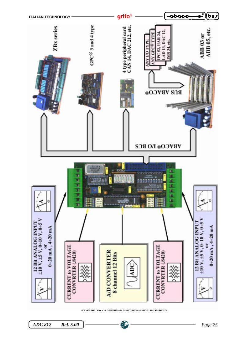
EXTERNAL CARDSEXTERNAL CARDS
ADC 812 can be connected to a wide range of block modules and operator interface system producedby grifo ®, or to many system of other companies.The on board resources can be expanded with asimple connection to the numerous peripheral grifo ® boards,both intelligent and not, thanks to itsstandard BUS ABACO® connector. Even cards with ABACO® I/O BUS can be connected, by usingthe proper mother boards.Hereunder some of these cards are briefly described; ask the detailed information directly to grifo ®,if required.
GPC® 323General Purpose Controller 51 family
80C32 µP, 14 MHz; Full CMOS; 1 RS 232 line (software); 1 RS 232 or RS 422-485 or Current Loopline; 24 TTL I/O lines; 11 A/D 12 bits lines; 3 Timers Counters; 64K EPROM; 64K RAM; 32K RAMand RTC backed; 32K DIL EEPROM; 8K serial EEPROM; Buzzer; 2 Activity LED; Watch dog; 5readable DIPs; LCD Interface.
GPC® 553General Purpose Controller 80C552
80C552 µP, 22÷33 MHz; 1 RS 232 line (software); 1 RS 232 or RS 422-485 or Current Loop line;16 TTL I/O lines; 8 A/D 10 bits lines; 3 Timers Counters; 64K EPROM; 64K RAM; 32K RAM andRTC backed; 32K DIL EEPROM; 8K serial EEPROM; 2 PWM lines; 1 Activity LED; Watch dog;5 readable DIPs; LCD Interface.
GPC® 153General Purpose Controller Z80
84C15 µP, 10÷16 MHz; Full CMOS; 1 RS 232 line; 1 RS 232 or RS 422-485 or Current Loop line;16 TTL I/O lines; 8 A/D 12 bits lines; 2÷4 Timers Counters; 512K EPROM or FLASH; 512K RAMand RTC backed; 8K serial EEPROM; Buzzer; 1 Activity LED; Watch dog; 8 readable DIPs; LCDInterface.
GPC® 183General Purpose Controller Z180
Z180 µP, 10÷16 MHz; Full CMOS; 1 RS 232 line; 1 RS 232 or RS 422-485 or Current Loop line;24 TTL I/O lines; 11 A/D 12 bits lines; 2 Timers Counters; 512K EPROM or FLASH; 512K RAMand RTC backed; 8K serial EEPROM; Buzzer; 2 Activity LED; Watch dog; 4 readable DIPs; LCDInterface.
GPC® 324/D“4” Type General Purpose Controller 80C32/320
80C32 or 80C320 µP, 14÷22 MHz; Full CMOS; 1 RS 232 line; 1 RS 232 or RS 422-485 or CurrentLoop line; 4÷16 TTL I/O lines; 3 Timers Counters; 64K EPROM; 64K RAM; 32K RAM backed;32K DIL E2; 8K serial EEPROM; Watch dog; 1 readable DIP; LCD Interface; Abaco® I/O BUS;5Vdc Power supply; Size: 100x50 mm.
ABB 03ABACO® Block BUS 3 slots
3 slots ABACO® mother board; 4 TE pitch connectors; ABACO® I/O BUS connector; screwterminal for power supply; connection for DIN C type and Ω rails.
grifo ® ITALIAN TECHNOLOGY
Page 24 ADC 812 Rel. 5.00
ABB 05ABACO® Block BUS 5 slots
5 slots ABACO® mother board with power supply. Double power supply built in; 5Vdc 2,5A sectionfor powering the on board logic; second section at 24Vdc 400mA galvanically coupled, for theoptocoupled input lines. Auxiliary connector for ABACO® I/O BUS. Connection for DIN Ω rails.
GPC® 554General Purpose Controller 80C552
Microprocessor 80C552 at 22 MHz; implementation completely CMOS; 32K EPROM; 32 KSRAM; 32 K EEPROM or SRAM; EEPROM; 2 RS 232 serial lines; 16 I/O TTL; 2 PWM lines; 16bits Timer/Counter; Watch Dog; 6 signals A/D converter with resolution 10 bit; interface forABACO® I/O BUS.
GPC® 154“4” Type General Purpose Controller Z80
84C15 µP, 10÷16 MHz; Full CMOS; 1 RS 232 line; 1 RS 232 or RS 422-485 line; 16 TTL I/O lines;2÷4 Timers Counters; 512K EPROM or FLASH; 512K RAM and RTC backed; 8K serial EEPROM;Watch dog; 2 readable DIPs; LCD Interface; Abaco® I/O BUS; 5Vdc Power supply; Size: 100x50mm.
GPC® 884General Purpose Controller Am188ES
Microprocessor AMD Am188ES up to 40 MHz16 bits; implementation completely CMOS; serie 4format; 512K EPROM or FLASH; 512K SRAM backed with Lithium battery; RTC; 1 RS 232 serialline + 1 RS 232 or RS 422-485 or current loop; 16 I/O TTL; 3 timer/counter; watch dog; EEPROM;11 signals A/D converter with 12 bit resolution; interface for ABACO® I/O BUS.
GPC® 114General Purpose Controller 68HC11
Microprocessor 68HC11A1 at 8 MHz; implementation completely CMOS; serie 4 format; 32KEPROM; 32K SRAM backed with Lithium battery; 32K EPROM, SRAM, EEPROM; RTC; 1 serialline RS 232 or RS 422-485; 10 I/O TTL; 3 timer/counter; watch dog; 8 signals A/D converter withresolution 8 bit; 1 asunchronous serial line; extremly low power consumption; interface forABACO® I/O BUS.
GPC® 184General Purpose Controller Z80195
Microprocessor Z80195 at 22 MHz; implementation completely CMOS; 512K EPROM or FLASH;512K RAM; Back-Up with Lithium battery internal or external; 1 serial line RS 232 + 1 RS 232 orRS 422-485 or current loop + 1 TTL; 18 I/O TTL; 4 timer/counter 8 bits; 2 timer 16 bits; Watch Dog;Real Time Clock; activity LED; EEPROM; interface for ABACO® I/O BUS.
GPC® AM4General Purpose Controller ATmega103
Microprocessor ATmega103 at 5.5 MHz; implementation completely CMOS; 128K internalFLASH; 32K SRAM; Back-Up with Lithium battery internal or external; 1 serial line RS 232 or RS422-485 or current loop; 16 I/O TTL; 8 linee A/D resolution 10 bits; 2 timer/counter; Watch Dog;Real Time Clock; 4K internal EEPROM; interface for ISP programming; interface forr ABACO®
I/O BUS.
ITALIAN TECHNOLOGY grifo ®
Page 25 ADC 812 Rel. 5.00
FIGURE 12: POSSIBLE CONNECTIONS DIAGRAM
grifo ® ITALIAN TECHNOLOGY
Page 26 ADC 812 Rel. 5.00
GPC® 51General Purpose Controller fam. 51
Microprocessor family 51 INTEL including the masked BASIC chip; the board features: 16 I/O TTLlines; dip switch; 3 timer/counter; RS 232; 4 A/D converter signals resolution 11 bit; buzzer; on boardEPROM programmer; RTC and 32K SRAM with Lithium battery back up; controlloer for displayand keyboard.
GPC® 188FGeneral Purpose Controller 80C188
80C188 µP 20MHz; 1 RS 232 line; 1 RS 232, RS 422-485 or Current Loop line; 24 TTL I/O lines;1M EPROM or 512K FLASH; 1M RAM Lithium battery backed; 8K serial EEPROM; RTC; WatchDog; 8 Dip switch; 3 Timer Counter; 8 13 bit A/D lines; Power failure; activity LEDs; single powersupply +5Vdc.
GPC® 15AGeneral Purpose Controller 84C15
Full CMOS card, 10÷20 MHz 84C15 CPU; 512K EPROM or FLASH; 128K RAM; 8K RAM andRTC backed; 8K serial EEPROM; 1 RS 232 line; 1 RS 232 line or RS 422-485 or Current Loop line;32 or 40 TTL I/O lines; CTC; Watch dog; 2 Dip switches; Buzzer.
GPC® 150General Purpose Controller 84C15
Microprocessor Z80 at 16 MHz; implementation completely CMOS; 512K EPROM or FLASH;512K SRAM; RTC; Back-Up through external Lithium battery; 4M serail FLASH ; 1 serial line RS232 plus 1 RS 232 or RS 422-485 or current loop; 40 I/O TTL; 2 timer/counter; 2 watch dog; dipswitch; EEPROM; A/D converter with resolution 12 bit; activity LED.
GPC® 15RGeneral Purpose Controller 84C15
84C15 µP, 10÷16 MHz; 1 RS 232 line; 1 RS 232 or RS 422-485 or C. L. line; 16÷24 TTL I/O lines;16 Opto-in; 8 Relays; 4 Opto Coupled Timers Counters; 512K EPROM or FLASH; 512K RAM andRTC backed; 8K serial EEPROM; 8K Backed RAM modul; Buzzer; 1 Activity LED; Watch dog;4÷12 readable DIPs; LCD Interface.
SPC 03.5SSwitch Power Card +5 Vdc
Europe format switching power supply capable to provide +5 Vdc to a load of 4 A; input voltage12÷24 Vac; power-failure; connector for back-up battery; standard connector for mother board SPB0x.
SPC 512Switch Power Card +5 Vdc +12 Vdc
Europe format switching power supply capable to provide +5 Vdc 5A and +12 Vdc 2.5 A; inputvoltage 12÷24 Vac; power-failure; connector for back-up battery; standard connector for motherboard SPB 0x.
ITALIAN TECHNOLOGY grifo ®
Page 27 ADC 812 Rel. 5.00
BIBLIOGRAPHYBIBLIOGRAPHY
Here follows a list of manuls thst can be a source of further informations about the devices installedon ADC 812.
Manual TEXAS INSTRUMENTES: The TTL Data Book - SN54/74 Families
Manual MAXIM: New Releases Data Book 1996 - Volume V
Manual NATIONAL SEMICONDUCTOR: DataBook - Linear 2
Please connect to the manifactures Web sites to get the latest version of all manuals and data sheets.

grifo ® ITALIAN TECHNOLOGY
Page 28 ADC 812 Rel. 5.00
ITALIAN TECHNOLOGY grifo ®
Page A-1 ADC 812 Rel. 5.00
APPENDIX A: ALPHABETICAL INDEXAPPENDIX A: ALPHABETICAL INDEX
SYMBOLS
+ 5VDC 15
A
A/D CONVERSION TIME 7A/D CONVERTER 4, 10, 12, 18, 19A/D CUT OFF FREQUENCY 7A/D EXAMPLE 20A/D INITIALIZATION SEQUENCE 22A/D INPUT IMPEDANCE 7A/D INPUTS 7, 14A/D INTERRUPT CONVERSION 22A/D POLLING CONVERSION 22A/D RESOLUTION 7A/D VOLTAGE POLARITY 20A/D VOLTAGE RANGE 20ABACO ® I/O BUS 7, 13, 15, 16, 22, 23ADDRESSING 6, 18ADDRESSING SPACE 7, 18
B
BIBLIOGRAPHY 27BLOCK DIAGRAM 5BUS 7BUS ABACO® 23BYTES TAKEN 7
C
CALIBRATION 8CARD VERSION 1CONNECTORS 7
CN1 13CN2 10CN3 12
CONSUMPTION 7
D
DASCTRL 19DASH 21DASL 20DIFFRENTIAL INPUT ERROR 7DIN 46277-1 AND 3 16DSW1 6, 17, 18
grifo ® ITALIAN TECHNOLOGY
Page A-2 ADC 812 Rel. 5.00
E
EXTERNAL CARDS 23
F
FILTERS 4
I
I/O CONNECTION 14INPUT FILTERS 4INTERFACING 6INTERRUPT 15, 16
J
JUMPERS 15
L
LINEARITY MAXIMUM ERROR 7
M
MAPPING 17MECHANICAL MOUNTING 16MOUNTING 16
O
OFFSET MAXIMUM ERROR 7ON BOARD RESOURCES 7OSCILLATOR FREQUENCY 7
P
POWER SUPPLY 7, 15
R
REFERENCE VOLTAGE 6RELATIVE HUMIDITY 7RESOURCES 7RV1 8
S
SIZE 7

ITALIAN TECHNOLOGY grifo ®
Page A-3 ADC 812 Rel. 5.00
T
TEMPERATURE RANGE 7TEST POINT 8TP1 8TRIMMER 8TTL 14
V
VOLTAGE REFERENCE 8VOLTAGE-CURRENT CONVERSION MODULE 14VREF 8
W
WEIGHT 7WORK FREQUENCY 7

grifo ® ITALIAN TECHNOLOGY
Page A-4 ADC 812 Rel. 5.00