
DISPOSITIVI ASIC Application Specific Integrated Circuit De Faveri Martina Classe 3 BET.

S.Veneziano, 2010, Roma
ASIC designTecnologie disponibili, flusso di progettazione.
Panoramica dei linguaggi utilizzati e librerie. Specifiche, partizionamento del progetto. Simulazione e
“testbench”. Sintesi logica. Vincoli di progetto. Analisi statica dei tempi, “floorplan” e vincoli alla sintesi fisica.
Piazzamento. Routing. Estrazione di resistenze e capacita’ parassite.
1
Friday, January 22, 2010
S.Veneziano, gennaio 2010, Roma
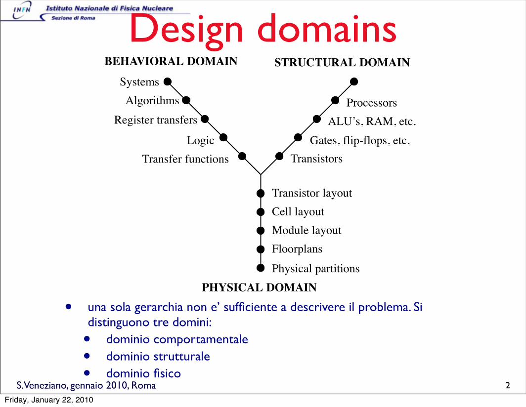
Design domains
• una sola gerarchia non e’ sufficiente a descrivere il problema. Si distinguono tre domini:
• dominio comportamentale
• dominio strutturale
• dominio fisico
BEHAVIORAL DOMAIN
PHYSICAL DOMAIN
Physical partitions
Floorplans
Module layout
Cell layout
Transistor layout
Systems
Algorithms
Register transfers
Logic
Transfer functions
Processors
ALU’s, RAM, etc.
Gates, flip-flops, etc.
Transistors
STRUCTURAL DOMAIN
2
Friday, January 22, 2010
S.Veneziano, gennaio 2010, Roma
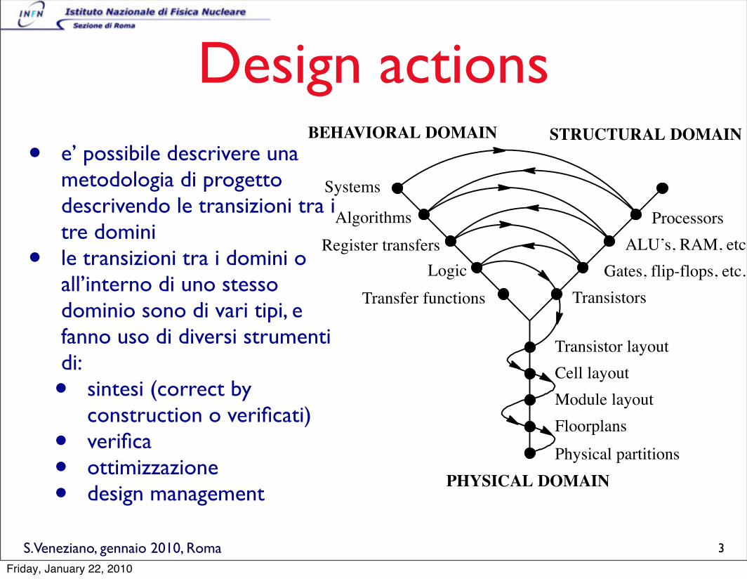
Design actions• e’ possibile descrivere una
metodologia di progetto descrivendo le transizioni tra i tre domini
• le transizioni tra i domini o all’interno di uno stesso dominio sono di vari tipi, e fanno uso di diversi strumenti di:• sintesi (correct by
construction o verificati)• verifica• ottimizzazione• design management
BEHAVIORAL DOMAIN
PHYSICAL DOMAIN
Physical partitions
Floorplans
Module layout
Cell layout
Transistor layout
Systems
Algorithms
Register transfers
Logic
Transfer functions
Processors
ALU’s, RAM, etc.
Gates, flip-flops, etc.
Transistors
STRUCTURAL DOMAIN
3
Friday, January 22, 2010

S.Veneziano, gennaio 2010, Roma
Design automation tools
• algorithmic and system design
• structural and logic design• transistor-level design• layout design• verification• design management• le soluzioni CMOS
disponibili oggi si differenziano per l’uso di un diverso set di tools di design automation
BEHAVIORAL DOMAIN
PHYSICAL DOMAIN
STRUCTURAL DOMAIN
Algorithmic and system design
Structural and logic design
Transistor-level design
Layout design
4
Friday, January 22, 2010

S.Veneziano, gennaio 2010, Roma
verification methods
• prototyping
• simulation
• formal verification (specification vs implementation)
5
Friday, January 22, 2010

S.Veneziano, gennaio 2010, Roma
Technologies and design approach
• soluzioni CMOS disponibili oggi:
• Full custom• Standard cell• Structured ASIC• Embedded array• Gate Array• Field Programmable Gate Array
• Hanno in comune la tecnologia della singola cella ma cambia il numero di maschere dedicate e il flusso di progettazione
6
Friday, January 22, 2010
S.Veneziano, gennaio 2010, Roma
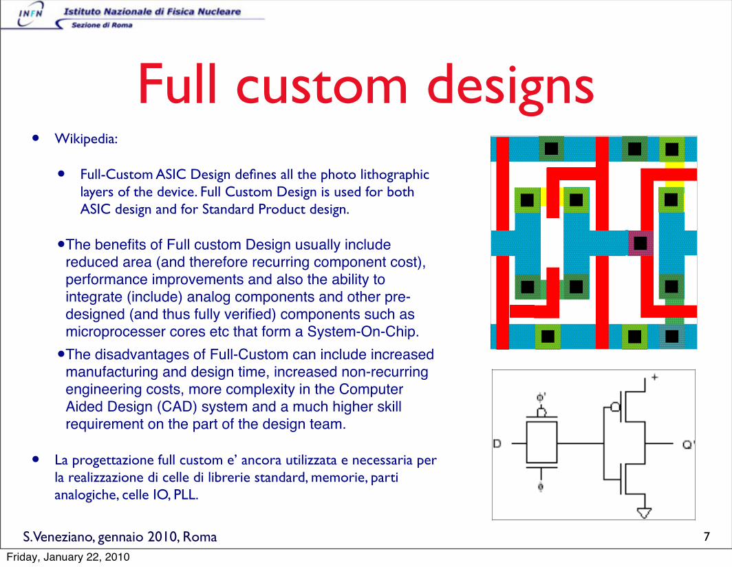
Full custom designs• Wikipedia:
• Full-Custom ASIC Design defines all the photo lithographic layers of the device. Full Custom Design is used for both ASIC design and for Standard Product design.
•The benefits of Full custom Design usually include reduced area (and therefore recurring component cost), performance improvements and also the ability to integrate (include) analog components and other pre-designed (and thus fully verified) components such as microprocesser cores etc that form a System-On-Chip.
•The disadvantages of Full-Custom can include increased manufacturing and design time, increased non-recurring engineering costs, more complexity in the Computer Aided Design (CAD) system and a much higher skill requirement on the part of the design team.
• La progettazione full custom e’ ancora utilizzata e necessaria per la realizzazione di celle di librerie standard, memorie, parti analogiche, celle IO, PLL.
7
Friday, January 22, 2010

S.Veneziano, gennaio 2010, Roma
Progetti full-custom
• in un progetto full-custom si fa uso di:
• layout editors (symbolic editor+compactors)
• design rule checkers
• circuit extractors (parasitics)
36 IC LAYOUT Chapter 3
Design-Rule Checking
Design rules were introduced in Chapter 2 as a set of layout restrictions that ensure the
manufactured design will operate as desired with no short or open circuits. A prime
requirement of the physical layout of a design is that it adhere to these rules. This can be
verified with the aid of a design-rule checker (DRC), which uses as inputs the physical
layout of a design and a description of the design rules presented in the form of a technol-
ogy file. Since a complex circuit can contain millions of polygons that must be checked
against each other, efficiency is the most important property of a good DRC tool. The ver-
ification of a large chip can take hours or days of computation time. One way of expedit-
ing the process is to preserve the design hierarchy at the physical level. For instance, if a
cell is used multiple times in a design, it should be checked only once. Besides speeding
up the process, the use of hierarchy can make error messages more informative by retain-
ing knowledge of the circuit structure.
DRC tools come in two formats: (1) The on-line DRC runs concurrent with the lay-
out editor and flags design violations during the cell layout. For instance, max has a built-
in design-rule checking facility. An example of on-line DRC is shown in Figure 3.4. (2)
Batch DRC is used as a post-design verifier, and is run on a complete chip prior to ship-
ping the mask descriptions to the manufacturer.
Circuit Extraction
Another important tool in the custom-design methodology is the circuit extractor, which
derives a circuit schematic from a physical layout. By scanning the various layers and
their interactions, the extractor reconstructs the transistor network, including the sizes of
the devices and the interconnections. The schematic produced can be used to verify that
the artwork implements the intended function. Furthermore, the resulting circuit diagram
contains precise information on the parasitics, such as the diffusion and wiring capaci-
tances and resistances. This allows for a more accurate simulation and analysis. The com-
plexity of the extraction depends greatly upon the desired information. Most extractors
extract the transistor network and the capacitances of the interconnect with respect to
GND or other network nodes. Extraction of the wiring resistances already comes at a
Figure 3.4 On-line design rule checking. The white dots
indicate a design rule violation. The violated rule can be
obtained with a simple mouse click.
poly_not_fet to all_diff minimum spacing = 0.14 um.
DMIA.fm Page 36 Monday, September 4, 2000 11:19 AM
Section 35
wires). The absolute coordinates of these elements are determined automatically by the
editor using a compactor [Hsueh79, Weste93]. The compactor translates the design rules
into a set of constraints on the component positions, and solves a constrained optimization
problem that attempts to minimize the area or another cost function.
An example of a symbolic notation for a circuit topology, called a sticks diagram, is
shown in Figure 3.2. The different layout entities are dimensionless, since only position-
ing is important. The advantage of this approach is that the designer does not have to
worry about design rules, because the compactor ensures that the final layout is physically
correct. Thus, she can avoid cumbersome polygon manipulations. Another plus of the
symbolic approach is that cells can adjust themselves automatically to the environment.
For example, automatic pitch-matching of cells is an attractive feature in module genera-
tors. Consider the case of Figure 3.3 (from [Croes88]), in which the original cells have dif-
ferent heights, and the terminal positions do not match. Connecting the cells would require
extra wiring. The symbolic approach allows the cells to adjust themselves and connect
without any overhead.
The disadvantage of the symbolic approach is that the outcome of the compaction
phase is often unpredictable. The resulting layout can be less dense than what is obtained
with the manual approach. Notwithstanding, symbolic layout tools have improved consid-
erably over the years and are currently a part of the mainstream design process.
Figure 3.2 Sticks representation of CMOS inverter. The numbers
represent the (Width/Length)-ratios of the transistors.
1
3
In Out
VDD
GND
Figure 3.3 Automatic pitch matching of datapath cells based on symbolic layout.
BEFORE
AFTER
DMIA.fm Page 35 Monday, September 4, 2000 11:19 AM
8
Friday, January 22, 2010
S.Veneziano, gennaio 2010, Roma
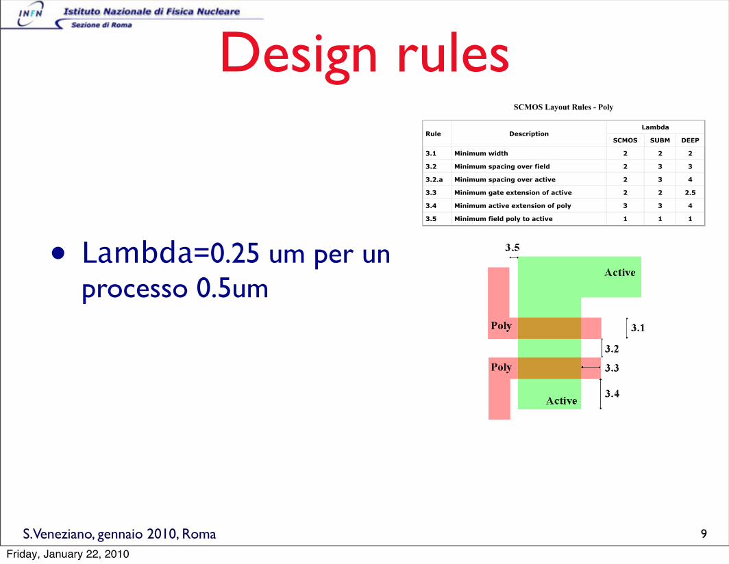
Design rules
• Lambda=0.25 um per un processo 0.5um
9
MOSIS SCMOS - Poly http://www.mosis.org/Technical/Designrules/scmos/scmos-poly.html
1 of 1 01/01/2005 16:13
SCMOS Layout Rules - Poly
Rule DescriptionLambda
SCMOS SUBM DEEP
3.1 Minimum width 2 2 2
3.2 Minimum spacing over field 2 3 3
3.2.a Minimum spacing over active 2 3 4
3.3 Minimum gate extension of active 2 2 2.5
3.4 Minimum active extension of poly 3 3 4
3.5 Minimum field poly to active 1 1 1
Friday, January 22, 2010

S.Veneziano, gennaio 2010, Roma
Standard cell design
• utilizziamo strumenti di piazzamento e routing, a partire da librerie di celle (gate-level)
10
Friday, January 22, 2010

S.Veneziano, gennaio 2010, Roma
Macrocelle e compilatori
• utilizzati nella progettazione standard cell
The eSi-RAM/2P two-port register file compiler is a high performance
memory solution for embedded applications. "What-if" scenarios are easy to
explore using the eSi-RAM/2P SRAM compiler helping designers to
perform optimal floorplanning of their designs.
Typical applications include register files, buffer memories, fall-through
FIFO’s, palette RAM’s, tag RAM etc. Wide bits make the memory very
suitable for address matching of physical and virtual addresses. Low area
overhead of decode-logic and sense-amplifiers are the salient features of the
two port compilers.
Key FeaturesKey Features! High performance – 650MHz for a 128x64 array! Synchronous read/write operations
! Dedicated read and write address ports
! Ports may be operated synchronously or independently
! Data retention at low voltage
! Zero standby current
! 3-State output buffers
! Byte-write control for selective data write! Ability to compile to multiple aspect ratios
! Interface to industry standard BIST controllers
Features Capability
Maximum Macro Size 64K
Maximum Words 1024
Minimum Words 8
Word Increment 2 * column mux
Maximum Data Width 128 bits
Minimum Data Width 4 bits
Data Width Increment 1 bit
Column Mux 1, 2, 4
Synthesis .libs (3 corners)
Behavioral Verilog, VITAL
Static Timing .libs
Place and Route LEF
Physical Views GDSII
Netlist HSPICE
Data Sheets Postscript, HTML
BenefitsBenefits
! High performance registerfiles
! Dedicated read & writeports operating withindependent clocks
! Java based compilerenhances ease-of-use and
automates EDA viewgeneration
! Accurate EDA modelingfor design integration
Data Preliminary Subject to Change Rev. 3.0
Copyright © 2000 Virtual Silicon Technology
All rights reserved
0.180.18mm eSiliconeSilicon Embedded Components Embedded Components
eSi-RAM/2P!!Two Port Register Compiler
0.18µµ L180 1.8V
High Performance Process
Silicon ReadySilicon Ready
! Engineered to foundry’sexact process for optimum
density and performance
! Proven test chips insure firsttime silicon success
! High resolution EDA modelsassure rapid timingconvergence
EDA VIEWS SUPPORT
0.18µµ L180, 1.8V
High Performance Process
In order to take advantage of the high intrinsic speed of advanced silicon
technologies, off-chip external clocks need to be multiplied to obtain high
on-chip frequencies. Many system-on-chip designs require multiple
application frequencies and therefore multiple PLL (Phase Locked Loop)
instances. The eSi-PLL is a compiler-based technology that allows systemdesigners to choose the center frequency, duty cycle, and create a
customized PLL. The PLL is created to be fully modular and embedded in
the I/O pad ring with no area overhead on the core. This also offers
complete modularity, eliminating manual wiring of analog power supply.
The PLL is best suited for applications such as frequency multiplication,
multi-phase clock generation, clock tree delay cancellation, clock
regeneration functions, duty cycle correction and jitter removal. The PLL
offers very high stability and good noise rejection characteristics, low power
consumption requiring no additional band-gaps or external components.
Key FeaturesKey Features! Compiler technology enhances ease-of-use! User provides 3 parameters – input, output frequencies and duty cycle
! Custom PLL has zero area overhead on core logic
! PLL module entirely located in the I/O pad rings
! Uses two dedicated analog power supply pine (AVDD, AVSS)
! Built-in ESD and latch-up protection structures
! Integrated loop filter and oscillator
! Integrated dividers are automatically programmed for duty cycle andinput clock division.
Parameters Capability
Input Frequency Range 14MHz to 200 MHz
Output Frequency Range 40MHz to 800MHz
Duty Cycle Range 33%, 50%, 66%
Max. long term jitter < 1% or 100ps
Synthesis (Black Box) .libs (3 corners)
Behavioral Verilog, VITAL
Static Timing .libs, TLF
Place and Route LEF, Frame-GDSII
Physical Views GDSII
Netlist HSPICE
Data Sheets PDF, HTML
BenefitsBenefits
! Wide frequency ranges to
meet multiple applicationrequirements
! Compiler technologygenerates customized PLL
! Module located inside I/Opad ring reduces die area
! Integrated loop filterensures high stability andnoise immunity
! Low Power
Data Preliminary Subject to Change Rev.3..0
Copyright © 2000 Virtual Silicon Technology
All rights reserved
0.180.18mm eSiliconeSilicon Embedded Components Embedded Components
eSi-PLL!!Phase Locked Loop Compiler
Silicon ReadySilicon Ready
! Engineered to foundry’sexact process for optimum
density and performance
! Proven test chips insure firsttime silicon success
! Ultra-high resolution of EDAmodels assures rapid timingconvergence
EDA Views Support
11
Friday, January 22, 2010
S.Veneziano, gennaio 2010, Roma
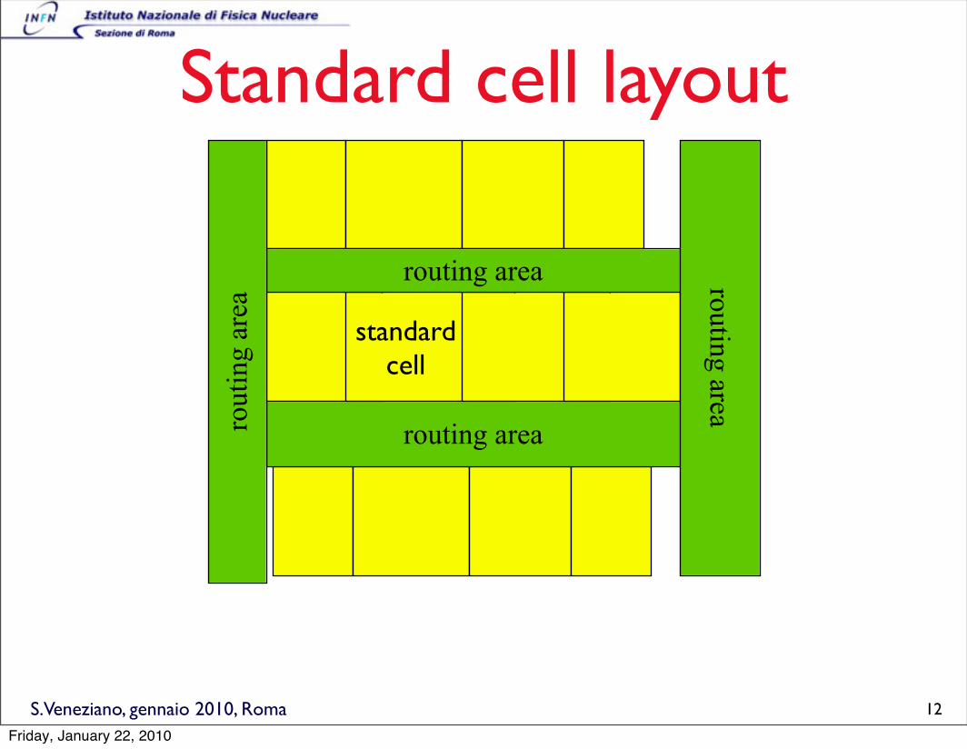
Standard cell layout
routing area
routing arearout
ing
area
routing area
12
standardcell
Friday, January 22, 2010

S.Veneziano, gennaio 2010, Roma
Gate array designs
• 2-4 layers di metallo dedicate al routing
• le dimensioni del die e il pincount sono predeterminati
Strong Technical SupportClose customer support provided by
NEC Electronics' global sales network.
Stable Delivery !Efficient production line operation
!Small-lot orders also delivered quickly
No.1 global
share since 1993Note
with
shipments exceeding
10,000 codes
Gate arrays are used to create a specific LSI by executing routing on a master wafer on which gates have been pre-placed in an
array formation.
The most beneficial feature of gate arrays is that a chip with the transistors embedded already exists, so only the routing process
needs to be carried out in order to realize (customize) the circuit. This means that a device can be developed much faster than a
full-custom or cell-based IC.
Products known as embedded arrays are also included in the gate array category. Embedded arrays are high-performance semi-
custom LSIs that use basic gate array cells in the internal area, but that feature embedded memories and cores of the same type
as cell-based ICs. When creating circuits with high-capacity memories, embedded arrays are the better option in terms of unit
price, but development will cost more in order to build the embedded array into the base wafer like cell-based ICs.
Don't hesitate to contact NEC Electronics for a quote to determine whether a gate array or embedded array is the better choice for
your design.
The Gate Array solution you don't want
No.1 global
share since 1993Note
with
shipments exceeding
10,000 codes
Extensive Product Lineup!Usable gates: 1.5 K to 1.5 M
!Power supply voltage: 5 V to 1.8 V
!Process: 0.5 m to 0.25 mµ µ
Note Source: Gartner Dataquest (April 2003)
2 Pamphlet A16841EJ2V0PF
"Low Cost" and "Time-to-Market" are the key demands that drive new
Now, master-slice-type products such as gate arrays have re-emerged as a
Your rivals are using gate array products. You can gain the edge by che
NEC
Product outlines
Basic Performance
PLL Macro Lineup
High-Speed I/O Lineup
Remark !: Not supported
µ
Parameter
Process
Wiring layers
Power supply voltage
Operating frequency
Usable gates
Package pin count
CMOS-N5
0.5 m
2-layer
2.7 to 5.5 V
5 V:60 MHz
3 V:33 MHz
1536 to 92538
20 to 304
EA-9HD
0.35 m
3/4-layer
2.7 to 3.6 V
100 MHz
9712 to 1386739
48 to 696
CMOS-10HD
0.25 m
3/4-layer
2.5/3.3 V
1.8/3.3 V
2.5 V:133 MHz
1.8 V:66 MHz
38143 to 1563458
44 to 680
Remark All series come complete with CTS and oscillation blocks. Scan path and boundary scan tests are also supported.
Note The input frequency is restricted to the range of 45 MHz " input frequency # internal multiplication factor setting " 100
MHz. Therefore, the minimum input frequency of approximately 6 MHz is supported only when the internal multiplication
factor is set to 8, and the maximum input frequency of 100 MHz is supported only when the internal multiplication factor is
set to 1.
Remark !: Not supported
Item
Skew adjustment DPLL
(F9E4)
Multiplication DPLL (F9H2)
Multiplication DPLL (F9H3)
Analog PLL
PLL for EMI noise
reduction:SSCG macro
CMOS-N5
!
!
!
!
!
CMOS-9HD
33 to 80
33 to 80
25 to 100
(Customer-specific support)
!
6 to 100Note
EA-9HD
33 to 80
33 to 80
25 to 100
(Customer-specific support)
4 to 160
6 to 100Note
CMOS-10HD
2.5 V: 33 to 133
1.8 V: 25 to 66
!
2.5 V: 33 to 133
1.8 V: 25 to 66
!
Under development
Input frequency (Unit: MHz)
Input/output frequency (Unit: MHz)
Item
PCI
GTL+
PECL
SSTL2
SSTL3
LVDS
CMOS-N5
VDD = 5.0 V
!
!
!
!
!
!
CMOS-9HD
VDD = 3.3 V
33/33
100/100
156/!
!
!
!
EA-9HD
VDD = 3.3 V
33/33
100/100
156/!
!
!
!
CMOS-10HD
VDD = 2.5 V
66/66
250/100
200/!
250/200
200/200
200/156
CMOS-9HD
0.35 m
3/4-layer
2.7 to 3.6 V
100 MHz
11207 to 1505570
48 to 696
µ µ µ
6 Pamphlet A16841EJ2V0PF
13
Friday, January 22, 2010

S.Veneziano, gennaio 2010, Roma
Embedded arrays, Structured ASICs
• come nei gate-arrays le maschere di diffusione sono comuni a tutti i progetti
• memorie, dll, microprocessori etc sono prediffusi.
• Migliori prestazioni rispetto ai gate array14
Friday, January 22, 2010

S.Veneziano, gennaio 2010, Roma
Metal layers
• i layers di metallo utilizzabili per le connessioni tra celle sono ridotti rispetto ad un progetto custom
• flessibilita’ sulle prestazioni (high-speed, low-power)
0.18µm ASIC Technology
Features
: SC82 and EA82 series
Overview
EA82 Embedded Array series is based on a 2P and 2N-
transistor basic cells (BC). It supports high-speed RAMs, ROMs,
CAM, mixed-signal macros, and a variety of other embedded
functions.
The EA82 series offers density (over 23 million total gates) and
provides the time-to-market advantage of gate arrays.
This series of devices include 44µm, 66µm, or 88µm pad pitch for
a cost-effective solution for both pad-limited and core-limited
designs.
With a nominal 1.1V to 1.8V core operation and with 2.5V
and 3.3Vand 5V tolerant I/Os, the EA82 series features a very
low-power consumption of 0.8 nW/gate/MHz.
Clk I/O
Hard
Macro
RAMs
SC82 Standard Cell library is optimized for synthesis-based
designs, and is designed for low power by improving transistor
count and minimizing crowbar current. Using optimized gates
instead of stacked transistors further minimizes power consump-
tion.
The core process operates at 1.1V to 1.8V with I/Os operating at
2.5V, 3.3V or 5V tolerant conditions. The library supports the
most popular third-party tools and data exchange file standards.
As with EA82, both standard and staggered I/O pad configura-
tions are supported. Interface options include low-swing, high-
speed I/Os and high-speed bus interface I/Os.
In addition to the traditional QFP packages, the SC82 family is
available in Ball Grid Array and Flip Chip packages.
CS81 offers a rich set of ADCs and DACs, digital and ana-log
PLLs, high-speed RAMs, ROMs and DRAMs, as well as
a variety of other embedded functions.
Standard Cell
(High Speed)
IP/Macro
(High Speed)
SRAM
Standard Cell
(Low Power)
IP/Macro
(Low Power)
Design Methodology
Fujitsu’s design methodology ensures first-silicon success by
integrating proprietary point tools with the most popular,
sign-off quality, industry-standard CAD tools. The following
are among these tools:
• Simultaneous Switching Output analysis
• Logic design rule checker
• 0.13µm effective channel length
• Up to 28 million gates per chip
• 3 to 5 layers of metal interconnects
• Very high density: 110K raw gates/mm 2
• 5 nW/gate/MHz power dissipation at 1.1V
• Core supply voltage: 1.1V to 1.8V
• 11 ps gate delay at 1.8V and 1 fan-out
• Junction temperation: -40 to 125oC
• I/Os: 3.3V, 2.5V, 1.8V, 5V tolerant
• High density diffused RAM, ROM, CAM
• High speed mixed signal macros, APLL
• Comprehensive list of high speed IO’s and popular standard
bus interface
• IPWareTM Soft IP and ARM7TDMI macro
• In-line and staggered IO in various pitches
• Advanced packaging support
• Proven design methodology and tool support
1.8V CMOS
2.5V CMOS
3.3V CMOS
5.0V TTL
1.8V Device
2.5V Device
3.3V Device
5.0V Device
1.8VCMOS
2.5VCMOS
3.3VCMOS
5.0VTolerant
PCI IEEE1394 USB
ADC/DAC
Cx81 Core
( 1.8V )
T-LVTTLP-CMLLVDSSDRAM I/FSSTLHSTLGTL +
High-speedInterface
High-speedDevices
AnalogInterface
PCI Bus IEEE1394 USB Devices
15
Friday, January 22, 2010

S.Veneziano, gennaio 2010, Roma
SOC architettureT Y P I C A L S O C D I E L A Y O U T
Embedded Microcontroller Coresfor system control and application support
MCU Peripheralscompatible with the MCU core
SRAM Cache Memoryfor rapid access to operational data
Industry-standard Interfacesfor networking and communication
Analog Interfacing and Processingfor direct connection to external devices
EEPROMData Memorygives instant
access to data
Flash ProgramMemory
eliminates the costand delay of ROM
code changes
EmbeddedDSP Core
for high-bandwidthsignal processing
Customer-specificLogic
that makesthe SoC unique
4B24 Silicon City 12 pg.xp 16/04/04 15:33 Page 10
16
Friday, January 22, 2010
S.Veneziano, gennaio 2010, Roma
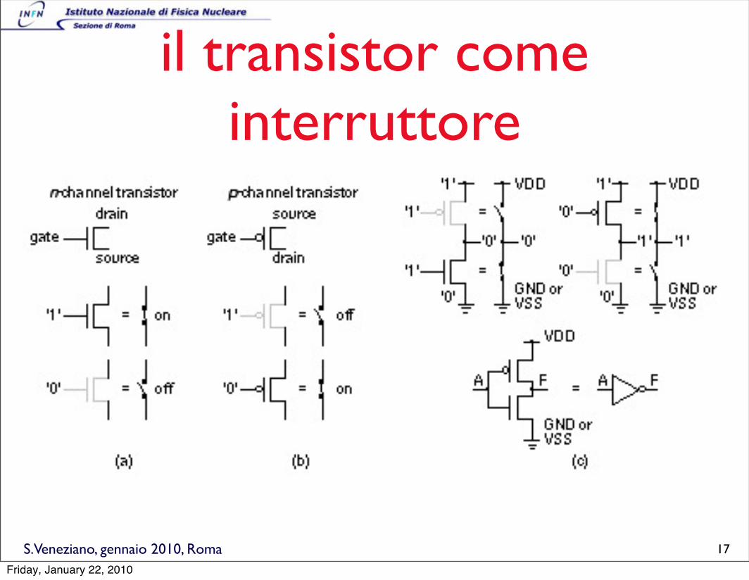
il transistor come interruttore
17
Friday, January 22, 2010

S.Veneziano, gennaio 2010, Roma
MOSIS 0.13 um MOSIS WAFER ACCEPTANCE TESTS RUN: T59M (8RF_8LM_DM) VENDOR: IBM-BURLINGTON TECHNOLOGY: SCN013 FEATURE SIZE: 0.13 microns Run type: SKD
INTRODUCTION: This report contains the lot average results obtained by MOSIS from measurements of MOSIS test structures on each wafer of this fabrication lot. SPICE parameters obtained from similar measurements on a selected wafer are also attached.
COMMENTS: 8RF_IBM-BURLIN
TRANSISTOR PARAMETERS W/L N-CHANNEL P-CHANNEL UNITS MINIMUM 0.16/0.12 Vth 0.41 -0.45 volts SHORT 20.0/0.12 Idss 462 -179 uA/um Vth 0.45 -0.45 volts Vpt 3.0 -3.9 volts WIDE 20.0/0.12 Ids0 277.7 -91.4 pA/um LARGE 50/50 Vth 0.11 -0.22 volts Vjbkd 2.6 -2.9 volts Ijlk <50.0 <50.0 pA Gamma 0.27 0.23 V^0.5 K' (Uo*Cox/2) 289.0 -49.3 uA/V^2 Low-field Mobility 535.64 91.37 cm^2/V*s
PROCESS PARAMETERS N+ P+ POLY M1 M2 M3 M4 UNITS Sheet Resistance 3.6 7.4 7.0 0.13 0.10 0.12 0.06 ohms/sq Contact Resistance 13.1 15.4 9.9 0.77 1.40 1.72 ohms Gate Oxide Thickness 32 angstrom PROCESS PARAMETERS M5 N+BLK PPLY+BLK M8 M6 POLY_NON TaN M7 N_W UNITS Sheet Resistance 0.06 75.7 328.2 0.01 0.09 1537.9 61.4 0.01 553 ohms/sq Contact Resistance 1.93 2.72 2.25 2.41 ohms COMMENTS: BLK is silicide block.
18
Friday, January 22, 2010
S.Veneziano, gennaio 2010, Roma
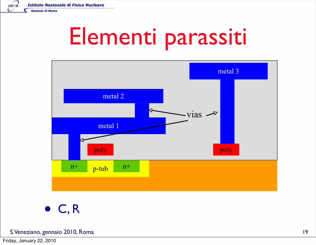
Elementi parassiti
• C, R
p-tub
poly poly
n+n+
metal 1
metal 3
metal 2
vias
19
Friday, January 22, 2010

S.Veneziano, gennaio 2010, Roma
Diffusioni
• formati dalle giunzioni p e n• n-type (0.5 μm process):
• bottomwall: 0.6 fF/μm2
• sidewall: 0.2 fF/μm
• p-type:
• bottomwall: 0.9 fF/μm2
• sidewall: 0.3 fF/μm
n+ (ND)
depletion region
substrate (NA)bottomwallcapacitance
sidewallcapacitances
20
Friday, January 22, 2010
S.Veneziano, gennaio 2010, Roma
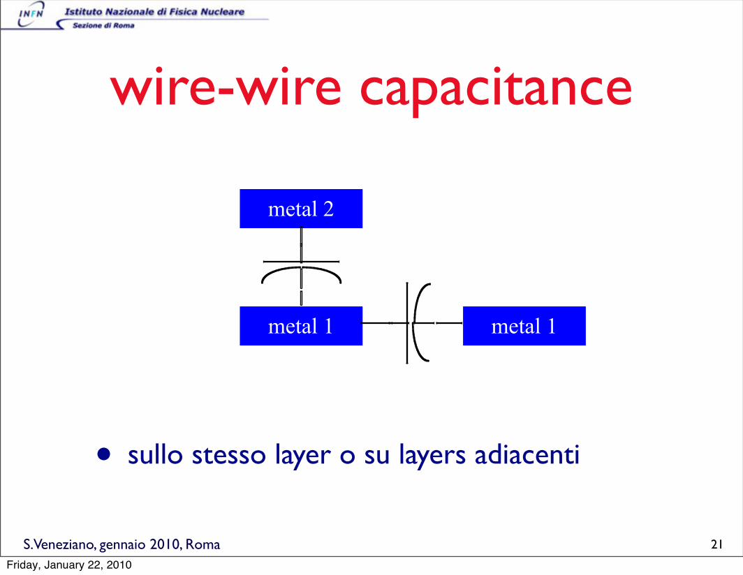
wire-wire capacitance
• sullo stesso layer o su layers adiacenti
metal 2
metal 1 metal 1
21
Friday, January 22, 2010

S.Veneziano, gennaio 2010, Roma
Resistenza
• R/square
Poly: 4 ohms/squaremetal 1: 0.08 ohms/squaremetal 2: 0.07 ohms/squaremetal 3: 0.03 ohms/squarendiff: 2 ohms/squarepdiff: 2 ohms/square
22
Friday, January 22, 2010

S.Veneziano, gennaio 2010, Roma
Propagation delays
• i modelli di timing possono essere piu’ complessi, come vedremo quando parleremo di timing verification.
23
Friday, January 22, 2010

S.Veneziano, gennaio 2010, Roma
Propagation delays 2
y = 0,7342x + 1,7317
R2 = 0,9999
0,00
5,00
10,00
15,00
20,00
25,00
30,00
35,00
0,00 10,00 20,00 30,00 40,00 50,00
timeLinear (time)
.OP
.TRAN 1NS 100NScl0 output0 Ground 5pFcl1 output1 Ground 10pFcl2 output2 Ground 20pFcl3 output3 Ground 40pF
VIN input Ground 0.01 PWL(0us 5V 10ns 5V 12ns 0V 20ns 0V)VGround 0 Ground DC 0VVdd +5V 0 DC 5Vm10 output0 input Ground Ground NMOS W=100u L=2um20 output0 input +5V +5V PMOS W=200u L=2um11 output1 input Ground Ground NMOS W=100u L=2um21 output1 input +5V +5V PMOS W=200u L=2um12 output2 input Ground Ground NMOS W=100u L=2um22 output2 input +5V +5V PMOS W=200u L=2um13 output3 input Ground Ground NMOS W=100u L=2um23 output3 input +5V +5V PMOS W=200u L=2u
.model nmos nmos level=2 vto=0.78 tox=400e-10 nsub=8.0e15 xj=-0.15e-6+ ld=0.20e-6 uo=650 ucrit=0.62e5 uexp=0.125 vmax=5.1e4 neff=4.0+ delta=1.4 rsh=37 cgso=2.95e-10 cgdo=2.95e-10 cj=195e-6 cjsw=500e-12+ mj=0.76 mjsw=0.30 pb=0.80.model pmos pmos level=2 vto=-0.8 tox=400e-10 nsub=6.0e15 xj=-0.05e-6+ ld=0.20e-6 uo=255 ucrit=0.86e5 uexp=0.29 vmax=3.0e4 neff=2.65+ delta=1 rsh=125 cgso=2.65e-10 cgdo=2.65e-10 cj=250e-6 cjsw=350e-12+ mj=0.535 mjsw=0.34 pb=0.80.end
time
voltage
XXX
0.0 5.0 10.0 15.0 20.0 25.0 30.0 35.0 40.0
ns
-1
0
1
2
3
4
5
V output3
time
voltage
XXX
0.0 5.0 10.0 15.0 20.0 25.0 30.0 35.0 40.0
ns
-1
0
1
2
3
4
5
V output0
24
Spice
Cload [pF]
delay [ns]
Friday, January 22, 2010
S.Veneziano, gennaio 2010, Roma
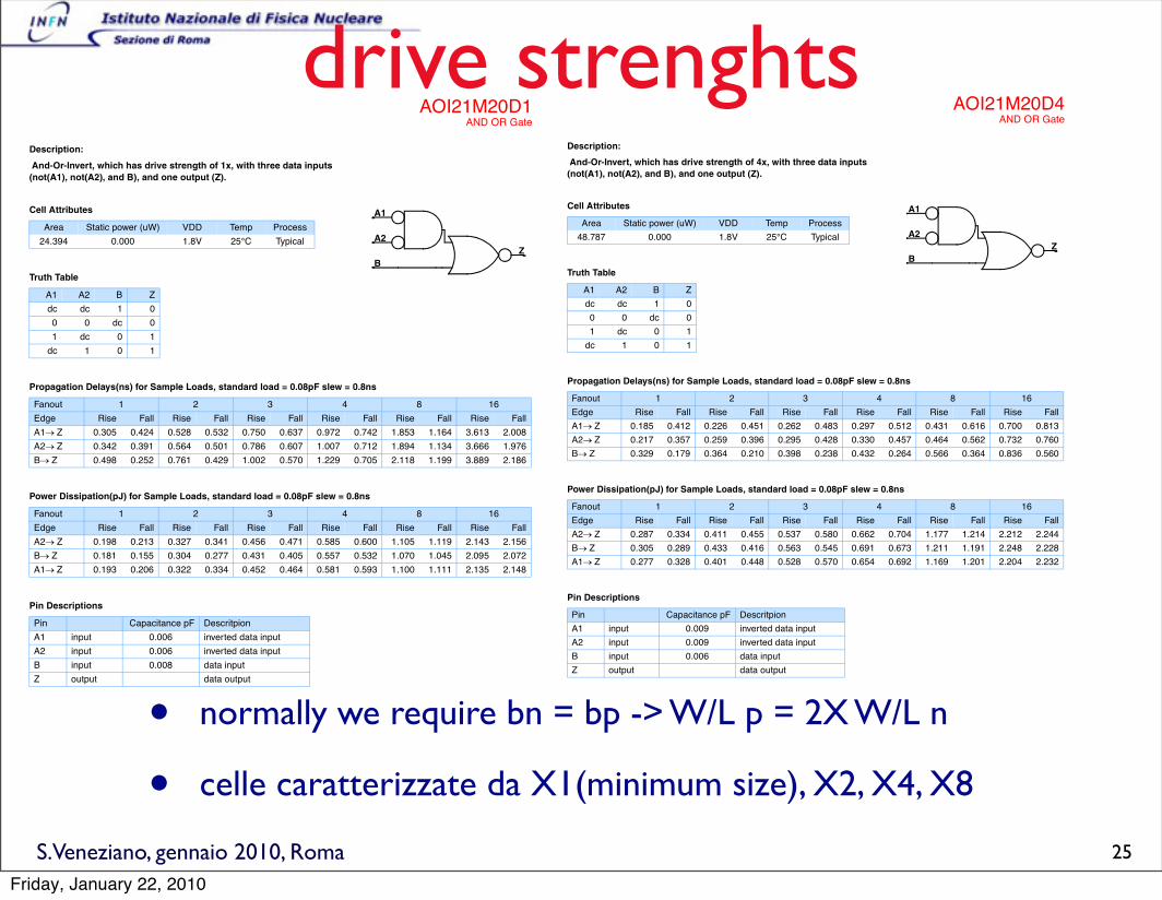
drive strenghts
• normally we require bn = bp -> W/L p = 2X W/L n
• celle caratterizzate da X1(minimum size), X2, X4, X8
AOI21M20D1AND OR Gate
© Virtual Silicon Technology, Inc. Any information in this databook is subject to change without notice.
0.18um Standard Cell Library 84
Description:
And-Or-Invert, which has drive strength of 1x, with three data inputs (not(A1), not(A2), and B), and one output (Z).
Cell Attributes
Area Static power (uW) VDD Temp Process
24.394 0.000 1.8V 25°C Typical
Truth Table
A1 A2 B Z
dc dc 1 0
0 0 dc 0
1 dc 0 1
dc 1 0 1
Propagation Delays(ns) for Sample Loads, standard load = 0.08pF slew = 0.8ns
Fanout 1 2 3 4 8 16
Edge Rise Fall Rise Fall Rise Fall Rise Fall Rise Fall Rise Fall
A1!"Z 0.305 0.424 0.528 0.532 0.750 0.637 0.972 0.742 1.853 1.164 3.613 2.008
A2!"Z 0.342 0.391 0.564 0.501 0.786 0.607 1.007 0.712 1.894 1.134 3.666 1.976
B!"Z 0.498 0.252 0.761 0.429 1.002 0.570 1.229 0.705 2.118 1.199 3.889 2.186
Power Dissipation(pJ) for Sample Loads, standard load = 0.08pF slew = 0.8ns
Fanout 1 2 3 4 8 16
Edge Rise Fall Rise Fall Rise Fall Rise Fall Rise Fall Rise Fall
A2!"Z 0.198 0.213 0.327 0.341 0.456 0.471 0.585 0.600 1.105 1.119 2.143 2.156
B!"Z 0.181 0.155 0.304 0.277 0.431 0.405 0.557 0.532 1.070 1.045 2.095 2.072
A1!"Z 0.193 0.206 0.322 0.334 0.452 0.464 0.581 0.593 1.100 1.111 2.135 2.148
Pin Descriptions
Pin Capacitance pF Descritpion
A1 input 0.006 inverted data input
A2 input 0.006 inverted data input
B input 0.008 data input
Z output data output
ZA2
A1
B
25
AOI21M20D4AND OR Gate
© Virtual Silicon Technology, Inc. Any information in this databook is subject to change without notice.
0.18um Standard Cell Library 86
Description:
And-Or-Invert, which has drive strength of 4x, with three data inputs (not(A1), not(A2), and B), and one output (Z).
Cell Attributes
Area Static power (uW) VDD Temp Process
48.787 0.000 1.8V 25°C Typical
Truth Table
A1 A2 B Z
dc dc 1 0
0 0 dc 0
1 dc 0 1
dc 1 0 1
Propagation Delays(ns) for Sample Loads, standard load = 0.08pF slew = 0.8ns
Fanout 1 2 3 4 8 16
Edge Rise Fall Rise Fall Rise Fall Rise Fall Rise Fall Rise Fall
A1!"Z 0.185 0.412 0.226 0.451 0.262 0.483 0.297 0.512 0.431 0.616 0.700 0.813
A2!"Z 0.217 0.357 0.259 0.396 0.295 0.428 0.330 0.457 0.464 0.562 0.732 0.760
B!"Z 0.329 0.179 0.364 0.210 0.398 0.238 0.432 0.264 0.566 0.364 0.836 0.560
Power Dissipation(pJ) for Sample Loads, standard load = 0.08pF slew = 0.8ns
Fanout 1 2 3 4 8 16
Edge Rise Fall Rise Fall Rise Fall Rise Fall Rise Fall Rise Fall
A2!"Z 0.287 0.334 0.411 0.455 0.537 0.580 0.662 0.704 1.177 1.214 2.212 2.244
B!"Z 0.305 0.289 0.433 0.416 0.563 0.545 0.691 0.673 1.211 1.191 2.248 2.228
A1!"Z 0.277 0.328 0.401 0.448 0.528 0.570 0.654 0.692 1.169 1.201 2.204 2.232
Pin Descriptions
Pin Capacitance pF Descritpion
A1 input 0.009 inverted data input
A2 input 0.009 inverted data input
B input 0.006 data input
Z output data output
ZA2
A1
B
Friday, January 22, 2010
S.Veneziano, gennaio 2010, Roma
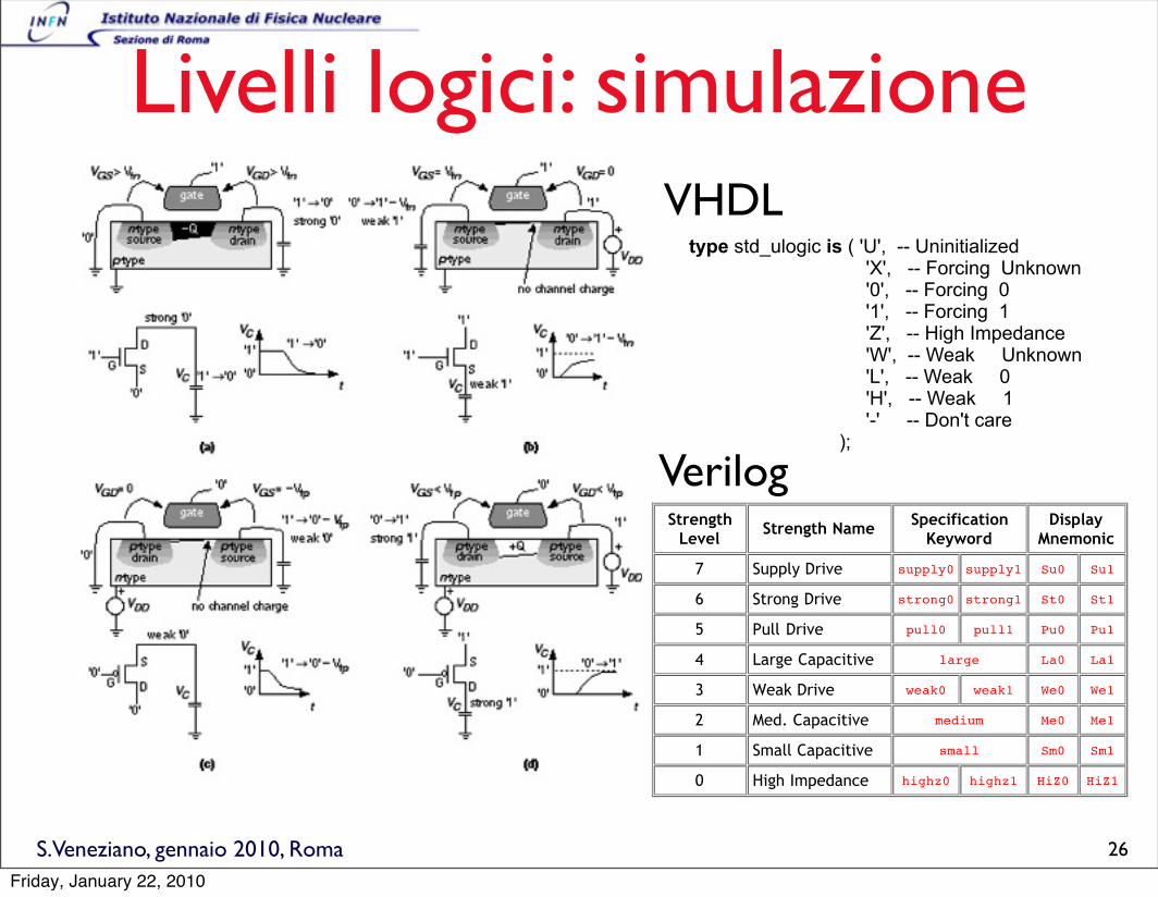
Livelli logici: simulazione
type std_ulogic is ( 'U', -- Uninitialized 'X', -- Forcing Unknown '0', -- Forcing 0 '1', -- Forcing 1 'Z', -- High Impedance 'W', -- Weak Unknown 'L', -- Weak 0 'H', -- Weak 1 '-' -- Don't care );
03/02/2006 11:02 AMVerilog HDL On-line Quick Reference body
Page 3 of 31http://www.sutherland-hdl.com/on-line_ref_guide/vlog_ref_body.html
x or X unknown or uninitialized
4.6 Logic Strengths
The Verilog HDL has 8 logic strengths: 4 driving, 3 capacitive, and high impedance (no strength).
Strength
LevelStrength Name
Specification
Keyword
Display
Mnemonic
7 Supply Drive supply0 supply1 Su0 Su1
6 Strong Drive strong0 strong1 St0 St1
5 Pull Drive pull0 pull1 Pu0 Pu1
4 Large Capacitive large La0 La1
3 Weak Drive weak0 weak1 We0 We1
2 Med. Capacitive medium Me0 Me1
1 Small Capacitive small Sm0 Sm1
0 High Impedance highz0 highz1 HiZ0 HiZ1
4.7 Literal Integer Numbers
Syntax
size'base valueSized integer in a specific radix
(base)
size (optional) is the number of bits in the number. Unsized integers default to at least 32-
bits.
'base (optional) represents the radix. The default base is decimal.
Base Symbol Legal Values
binary b or B 0, 1, x, X, z, Z, ?, _
octal o or O 0-7, x, X, z, Z, ?, _
decimal d or D 0-9, _
hexadecimal h or H 0-9, a-f, A-F, x, X, z, Z, ?, _
The ? is another way of representing the Z logic value.
An _ (underscore) is ignored (used to enhance readability).
Values are expanded from right to left (lsb to msb).
When size is less than value, the upper bits are truncated.
When size is larger than value, and the left-most bit of value is 0 or 1, zeros are left-
extended to fill the size.
When size is larger than value, and the left-most bit of value is Z or X, the Z or X is left-
26
Verilog
VHDL
Friday, January 22, 2010

S.Veneziano, gennaio 2010, Roma
Design libraries
• simulation
• synthesis
• place and routing
• testvector generation
27
Friday, January 22, 2010
S.Veneziano, gennaio 2010, Roma
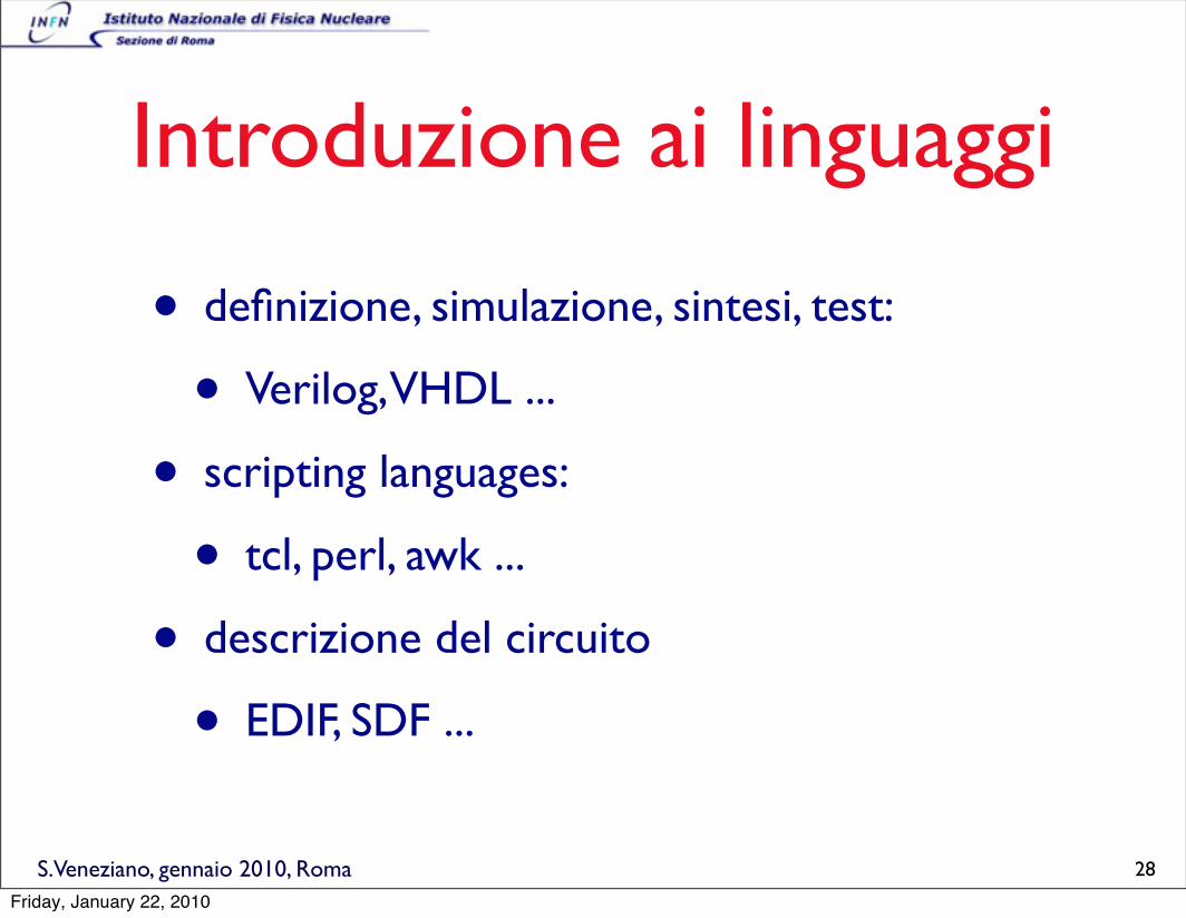
Introduzione ai linguaggi
• definizione, simulazione, sintesi, test:
• Verilog, VHDL ...
• scripting languages:
• tcl, perl, awk ...
• descrizione del circuito
• EDIF, SDF ...
28
Friday, January 22, 2010
S.Veneziano, gennaio 2010, Roma
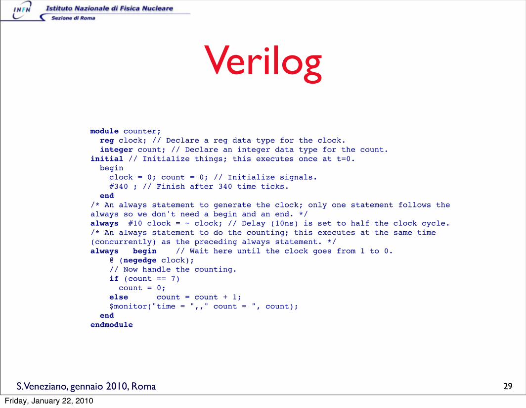
Verilogmodule counter; reg clock; // Declare a reg data type for the clock. integer count; // Declare an integer data type for the count.initial // Initialize things; this executes once at t=0. begin clock = 0; count = 0; // Initialize signals. #340 ; // Finish after 340 time ticks. end /* An always statement to generate the clock; only one statement follows the always so we don't need a begin and an end. */always #10 clock = ~ clock; // Delay (10ns) is set to half the clock cycle./* An always statement to do the counting; this executes at the same time (concurrently) as the preceding always statement. */always begin // Wait here until the clock goes from 1 to 0. @ (negedge clock); // Now handle the counting. if (count == 7) count = 0; else count = count + 1; $monitor("time = ",," count = ", count); end endmodule
29
Friday, January 22, 2010

S.Veneziano, gennaio 2010, Roma
Esempi di celle di libreria// // Copyright (C) 2001 Virtual Silicon Technology Inc.. All Rights Reserved. // "eSilicon", "eSi", "eSi-Route", "eSi-Pad", "eSi-RAM", "eSi-ROM", "eSi-PLL", // "The Heart of Great Silicon(R)", "Silicon Ready(R)", "IP Ambassador", // "Design Service Ambassador", and "Virtual Silicon" are trademarks // of Virtual Silicon Technology Inc. // // Virtual Silicon Technology Inc. // 1200 Crossman Ave Suite 200 // Sunnyvale, CA 94089-1116 // Phone : 408-548-2700 // Fax : 408-548-2750 // Web Site : www.virtual-silicon.com // // File Name: DFFPB1.v // Library Name: umcl18u250t2 // Library Release: 2.1 // Process: eSi/Route-11 UMC L180 // verigen patch-level 1.132-m 02/27/2000 13:49:14`celldefine// Positive Edge, D Flip-Flop; Q, QB Outputs// Q = rising(CK) ? D : 'p';QB = !Qmodule DFFPB1 (Q, QB, CK, D); output Q; output QB; input CK; input D; reg notifier; p_ff _i0 (Q, D, CK, notifier); not _i1 (QB,Q); specify (CK => Q) = (1,1); (CK => QB) = (1,1);`ifdef no_tchk`else $hold(posedge CK,negedge D,0,notifier); $hold(posedge CK,posedge D,0,notifier); $setup(negedge D,posedge CK,0,notifier); $setup(posedge D,posedge CK,0,notifier); $width(negedge CK,1,0,notifier); $width(posedge CK,1,0,notifier);`endif endspecifyendmodule`endcelldefine
// POSITIVE EDGE TRIGGERED D FLIP-FLOPprimitive p_ff (Q, D, CP,notifier); output Q; reg Q; input D, CP,notifier;
table // D CP No : Qt : Qt+1 1 (01) ? : ? : 1; // clocked data 0 (01) ? : ? : 0; 1 (x1) ? : 1 : 1; // reducing pessimism 0 (x1) ? : 0 : 0; 1 (bx) ? : 1 : 1; 0 (bx) ? : 0 : 0; ? (?0) ? : ? : -; * b ? : ? : -; // ignore edges on data ? ? * : ? : x; endtableendprimitive
30
Friday, January 22, 2010

S.Veneziano, gennaio 2010, Roma
Esempi di file SDF(DELAYFILE(SDFVERSION "OVI 2.1")...(DIVIDER /)// OPERATING CONDITION "BEST::WORST"(VOLTAGE 1.98::1.62)(PROCESS "1.000::1.000")(TEMPERATURE 0.00::125.00)(TIMESCALE 1ns)(CELL (CELLTYPE "cma_io") (INSTANCE) (DELAY (ABSOLUTE (INTERCONNECT U110/Z out_k_31/DO (0.016::0.016) (0.015::0.016)) (INTERCONNECT U116/Z out_k_30/DO (0.022::0.022) (0.021::0.022)) (INTERCONNECT U122/Z out_k_29/DO (0.022::0.023) (0.022::0.023)) (INTERCONNECT U134/Z out_k_28/DO (0.022::0.022) (0.022::0.023)) (INTERCONNECT U41/Z out_k_27/DO (0.013::0.013) (0.013::0.013))...(CELL (CELLTYPE "DFFRPB2") (INSTANCE muxb/clockb/divout_reg)
(DELAY (ABSOLUTE (IOPATH RB Q () (0.278:0.278:0.278)) (IOPATH CK Q (0.481:0.481:0.481) (0.452:0.452:0.452)) (IOPATH RB QB (0.381:0.381:0.381) ()) (IOPATH CK QB (0.566:0.566:0.566) (0.595:0.595:0.595)) ) ) (TIMINGCHECK (SETUP (posedge D) (COND shcheckCKDlh === 1'b1 (posedge CK)) (0.115:0.115:0.115)) (SETUP (negedge D) (COND shcheckCKDlh === 1'b1 (posedge CK)) (0.017:0.017:0.017)) (HOLD (posedge D) (COND shcheckCKDlh === 1'b1 (posedge CK)) (0.000:0.000:0.000)) (HOLD (negedge D) (COND shcheckCKDlh === 1'b1 (posedge CK)) (0.010:0.010:0.010)) (WIDTH (negedge RB) (0.338:0.338:0.338)) (RECOVERY (posedge RB) (posedge CK) (-0.304:-0.304:-0.304)) (HOLD (posedge RB) (posedge CK) (0.356:0.356:0.356)) (WIDTH (negedge CK) (0.267:0.267:0.267)) (WIDTH (posedge CK) (0.236:0.236:0.236)) ))
31
Friday, January 22, 2010

S.Veneziano, gennaio 2010, Roma
high-level libraries
• esempio:FIFO
DesignWare IP Family
Memory – FIFO Overview
192 Synopsys, Inc. December 12, 2005
Memory – FIFO OverviewThe FIFOs in this category address a broad array of design requirements. FIFOs, which include dual-port RAM memory arrays, are offered for both synchronous and asynchronous interfaces. The memory arrays are offered in two configurations: latch-based to minimize area, and D flip-flop-based to maximize testability. These two configurations also offer flexibility when working under design constraints, such as a requirement that no latches be employed. Flip-flop-based designs employ no clock gating to minimize skew and maximize performance. All FIFOs employ a FIFO RAM controller architecture in which there is no extended “fall-through” time required before reading contents just written.
Also offered are FIFO Controllers without the RAM array. They consist of control and flag logic and an interface to common ASIC dual port RAMs. Choosing between the two is typically based on the required size of the FIFO. For shallow FIFOs (less than 256 bits), synchronous or asynchronous FIFOs are available which include both memory and control in a single macro. These macros can be programmed via word width, depth, and level (almost-full flag) parameters.
For larger applications (greater than 256 bits), you can use the asynchronous FIFO Controller with a diffused or metal programmable RAM. See Figure 1.
Figure 1: Memory: FIFOs and FIFO Controllers
All FIFOs and Controllers support full, empty, and programmable flag logic. Programmable flag logic may be statically or dynamically programmed. When statically programmed, the threshold comparison value is hardwired at synthesis compile time. When dynamically programmed, it may be changed during FIFO operation.
DiffusedorMetal ProgrammableRAM(on-chip or off-chip)
Synthetic DesignsFIFO RAM Controller
Synthetic Designs FIFO(includes control and memory)
Controller
LatchorFlip-FlopBased RAM
FIFO Controller to be used with a technology-specific vendor supplied RAM
Technology-independent FIFOthat includes control and memory
•For large FIFOs (> 256 bits)•Interfaces to dual port static RAMs
•For shallow FIFOs (< 256 bits)•Self-contained RAM storage array
December 12, 2005 Synopsys, Inc. 193
DesignWare IP Family
DW_asymfifo_s1_dfAsymmetric I/O Synchronous (Single Clock) FIFO with Dynamic Flag
DW
L Sythesizable IP
DW_asymfifo_s1_dfAsymmetric I/O Synchronous (Single Clock) FIFO with Dynamic Flag
! Fully registered synchronous flag output ports
! D flip-flop-based memory array for high testability
! All operations execute in a single clock cycle
! FIFO empty, half full, and full flags
! Parameterized asymmetric input and output bit widths (must be integer-multiple relationship)
! Word integrity flag for data_in_width < data_out_width
! Flushing out partial word for data_in_width < data_out_width
! Parameterized byte (or subword) order within a word
! FIFO error flag indicating underflow, overflow, and pointer corruption
! Parameterized word depth
! Dynamically programmable almost full and almost empty flags
! Parameterized reset mode (synchronous or asynchronous, memory array initialized or not)
push_req_n
full
emptyerror
data_out
pop_req_n
diag_n
rst_nclk
almost_full
half_full
almost_empty
data_in
flush_n
ram_full
part_wdae_level
af_thresh
32
Friday, January 22, 2010

S.Veneziano, gennaio 2010, Roma
Macrocell libraries
• encapsulationlibrary IEEE;use IEEE.std_logic_1164.all;use IEEE.VITAL_timing.all;
library umc;use umc.all;
library work;use work.cma_common.all;
entity cma_pll is port ( clk40 : in STD_LOGIC; -- Input clock bypass : in STD_LOGIC; -- pass thru enable clr : in STD_LOGIC; -- Reset not lock : out STD_LOGIC; -- PLL is in lock clk : out STD_LOGIC -- PLL clock out );end cma_pll;
architecture rtl of cma_pll is component PLL40x320x6LM port ( REF : in STD_LOGIC; -- Input clock FB : in STD_LOGIC; -- Feedback from a delayed place on the chip BYPASS : in STD_LOGIC; -- pass thru mode enable RESET : in STD_LOGIC; -- Reset not LOCK : out STD_LOGIC; -- PLL is in lock PLLOUT : out STD_LOGIC -- PLL clock out ); end component; signal int_clr : STD_LOGIC; signal int_clk : STD_LOGIC;begin clk <= int_clk; clear : process(clr) begin if CLRVAL = '1' then int_clr <= clr; else int_clr <= not clr; end if; end process; pll : PLL40x320x6LM port map ( REF => clk40, FB => int_clk, BYPASS => bypass, RESET => int_clr, LOCK => lock, PLLOUT => int_clk);end rtl;
33
Friday, January 22, 2010

S.Veneziano, gennaio 2010, Roma
Il progetto di un ASIC
• Documento specifiche
• “package” di parametri
• utilizzato anche nella simulazione comportamentale
--*****************************************************--* file: cma_common.vhd--* Package: cma_common--*--* basic package for cma, contains main parameters--* @author : S. Veneziano, R.Vari--* @version 1.0 : 20001001 : birth--*****************************************************--/
library IEEE;library DWARE;use IEEE.NUMERIC_STD.all;use DWARE.DWpackages.all;use IEEE.STD_LOGIC_1164.all;
package cma_common is
--* ASIC identification bit size constant CMA_DEVID_SIZE : integer := 7;
constant SERIALWSIZE : integer := 16; -- serialized data word size
--* I2C register sizes are modulo 8 constant I2CMOD : integer := 8;
--* BC Counter size constant FEBCID_WIDTH : integer := 12;
--* L1ID Counter size constant FEL1ID_WIDTH : integer := 9;
--* Frontend grouping --* in number of strips constant FE_GROUP : integer := 8;
--* deadtime setting of input signals --* in number of time slices constant FE_DEADTIME : integer := 32;
34
Friday, January 22, 2010

S.Veneziano, gennaio 2010, Roma
Behavioral modelmodule fifo( dout, // head of fifo full, // no more space, no shift-in allowed half, // fifo is >=50% full quarter, // fifo is >=25% full empty, // head of fifo is invalid data clk, res_, din, // data to store shiftin, // store data from din in fifo shiftout); // i've read the head of fifo, show me next
parameter WIDTH = 32; // bit width parameter DEPTH = 16; // depth of fifo
output [(WIDTH-1):0] dout; output full, half, quarter, empty; reg full, half, quarter, empty; input clk, res_, shiftin, shiftout; input [(WIDTH-1):0] din;
reg [(WIDTH-1):0] entry [0:(DEPTH-1)]; // the register stages integer wp; // write pointer (points to first free slot) integer i; // loop count
// first stage of fifo is output assign dout = entry[0];
always @(posedge clk or negedge res_) // trigger new evaluation begin if (res_ == 0) // it's a reset begin wp = 0; // the initial values full <= 1'b0; half <= 1'b0; quarter <= 1'b0; empty <= 1'b1; end else // it's a posedge of clk begin case ({shiftin, shiftout}) 2'b00: ; // nothing to do 2'b01: // shift-out(assumes: at least 1 valid value in fifo) begin for (i=1; i<wp; i=i+1) // shift all valid entries entry[i-1] <= entry[i]; wp = wp-1; full <= 1'b0; half <= (wp >= (DEPTH/2)) ? 1'b1 : 1'b0; quarter <= (wp >= (DEPTH/4)) ? 1'b1 : 1'b0; empty <= (wp == 0) ? 1'b1 : 1'b0; end 2'b10: // shift-in (assumes: at least 1 entry free) begin entry[wp] <= din; wp = wp+1; full <= (wp == DEPTH) ? 1'b1 : 1'b0; half <= (wp >= (DEPTH/2)) ? 1'b1 : 1'b0; quarter <= (wp >= (DEPTH/4)) ? 1'b1 : 1'b0; empty <= 1'b0; end 2'b11: //simultaneous shift-in and -out begin // (at least 1 valid entry) for (i=1; i<wp; i=i+1) entry[i-1] <= entry[i]; entry[wp-1] <= din; end endcase // case ({shiftin, shiftout}) end // else: !if(res_ == 0) end // always @ (posedge clk or negedge res_)
endmodule35
Friday, January 22, 2010
S.Veneziano, gennaio 2010, Roma
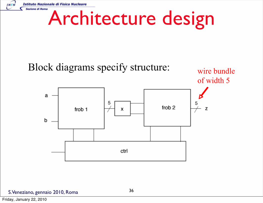
Architecture design
Block diagrams specify structure: wire bundleof width 5
36
Friday, January 22, 2010

S.Veneziano, gennaio 2010, Roma
System Partitioning
• Il sistema va partizionato in base a:
• funzionalita’
• constraints di sintesi
• constraints fisici
• risorse umane disponibili
37
Friday, January 22, 2010

S.Veneziano, gennaio 2010, Roma
rtl model
A register-transfer machine has combinationallogic connecting registers:
DQ combinationallogic
D QD Q combinationallogic
combinationallogic
38
Friday, January 22, 2010
S.Veneziano, gennaio 2010, Roma
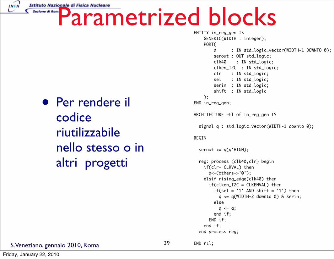
Parametrized blocks
• Per rendere il codice riutilizzabile nello stesso o in altri progetti
ENTITY in_reg_gen IS GENERIC(WIDTH : integer); PORT( a : IN std_logic_vector(WIDTH-1 DOWNTO 0); serout : OUT std_logic; clk40 : IN std_logic; clken_I2C : IN std_logic; clr : IN std_logic; sel : IN std_logic; serin : IN std_logic; shift : IN std_logic );END in_reg_gen;
ARCHITECTURE rtl of in_reg_gen IS
signal q : std_logic_vector(WIDTH-1 downto 0);
BEGIN
serout <= q(q'HIGH); reg: process (clk40,clr) begin if(clr= CLRVAL) then q<=(others=>'0'); elsif rising_edge(clk40) then if(clken_I2C = CLKENVAL) then if(sel = '1' AND shift = '1') then q <= q(WIDTH-2 downto 0) & serin; else q <= a; end if; END if; end if; end process reg;
END rtl;39
Friday, January 22, 2010

S.Veneziano, gennaio 2010, Roma
La simulazione
• possiamo distinguere almeno due tipi:
• Compiler driven
• Event driven
40
Friday, January 22, 2010
S.Veneziano, gennaio 2010, Roma
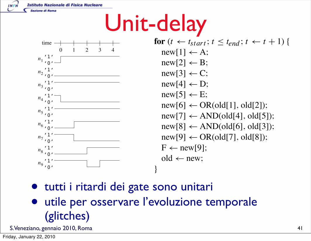
Unit-delay
• tutti i ritardi dei gate sono unitari
• utile per osservare l’evoluzione temporale (glitches)
time
’0’
’1’
’0’
’1’
0 1 2 3 4
n1
n2
n3
n4
n5
n6
n7
n8
n9
’0’
’1’
’0’
’1’
’0’
’1’
’0’
’1’
’0’
’1’
’0’
’1’
’0’
’1’
for (t ! tstart ; t " tend ; t ! t + 1) {new[1]! A;
new[2]! B;
new[3]! C;
new[4]! D;
new[5]! E;
new[6]! OR(old[1], old[2]);
new[7]! AND(old[4], old[5]);
new[8]! AND(old[6], old[3]);
new[9]! OR(old[7], old[8]);
F! new[9];
old! new;
}
41
Friday, January 22, 2010

S.Veneziano, gennaio 2010, Roma
Simulazione event-driven
• utilizzata nei simulatori gate-level.
• un evento e’ un cambiamento di livello di un segnale ad un certo tempo
• un evento puo’ causare la variazione di livello di altri segnali
struct event {int time;
struct net *node;
struct signal value value;
. . .
};
struct event queue {. . .
};
struct event queue *new queue();
{“create an empty event queue”;
}
struct event *first event(struct event queue *queue)
{“remove the earliest event from an event queue and return it”;
}
insert event(struct event queue *queue, struct event *new event)
{“add a given event to an event queue”;
}
42
Friday, January 22, 2010

S.Veneziano, gennaio 2010, Roma
Delta-cycles
• Eventi vengono inseriti nella coda, ordinati secondo il tempo di aggiornamento del segnale
• Eventi possono essere distanziati di un tempo di simulazione determinato dai gate delays o nullo (delta cycle)
time
current
time
(n! 1)!t
n!t
(n" 1)!t
(n" 2)!t
(n" 3)!t
43
Friday, January 22, 2010

S.Veneziano, gennaio 2010, Roma
Testbench organization
• modello idealeEE495D Fall 2004 Test and Debug Page 13
Gold Model Approach
GoldModel
DUT
InputPatternGenerator
Fail
XOR each pair ofoutput bits individually
Test Bench
44
Friday, January 22, 2010
S.Veneziano, gennaio 2010, Roma
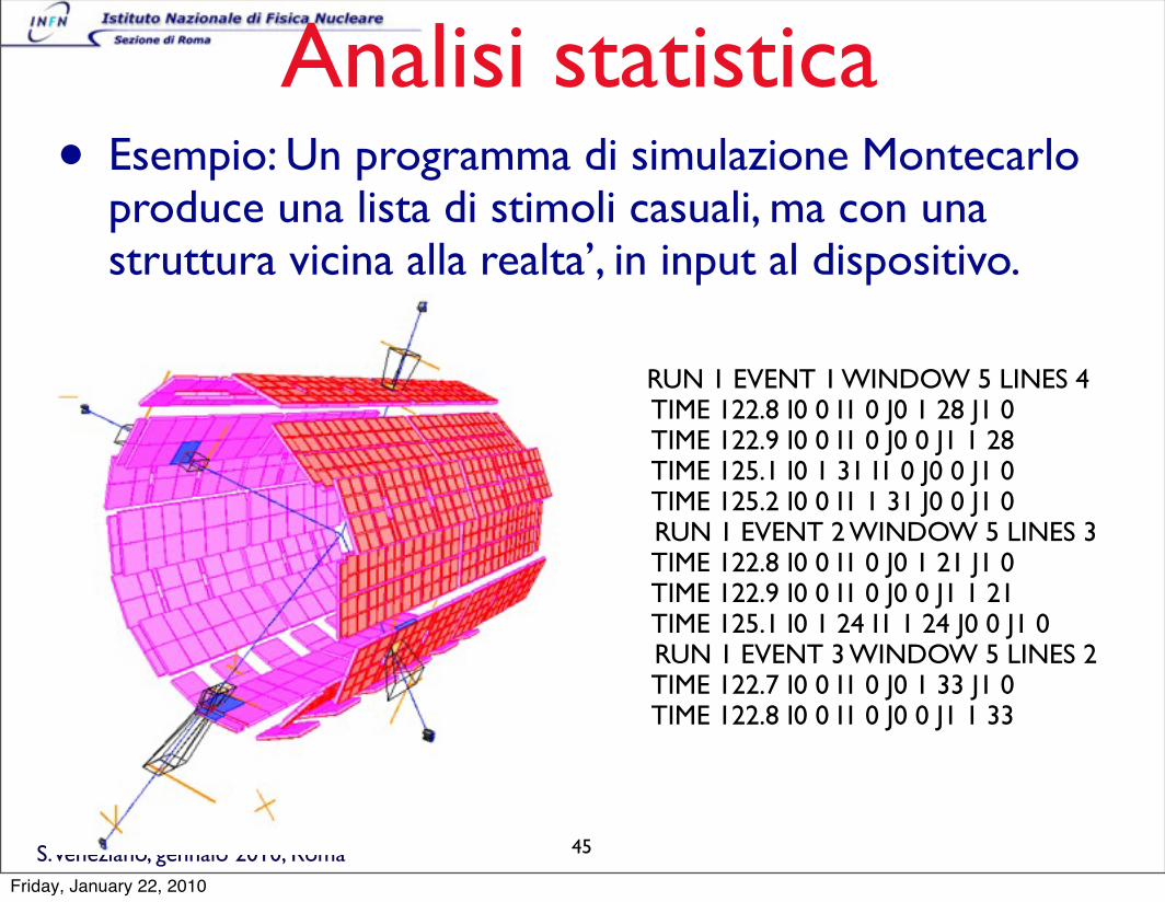
Analisi statistica• Esempio: Un programma di simulazione Montecarlo
produce una lista di stimoli casuali, ma con una struttura vicina alla realta’, in input al dispositivo.
RUN 1 EVENT 1 WINDOW 5 LINES 4 TIME 122.8 I0 0 I1 0 J0 1 28 J1 0 TIME 122.9 I0 0 I1 0 J0 0 J1 1 28 TIME 125.1 I0 1 31 I1 0 J0 0 J1 0 TIME 125.2 I0 0 I1 1 31 J0 0 J1 0 RUN 1 EVENT 2 WINDOW 5 LINES 3 TIME 122.8 I0 0 I1 0 J0 1 21 J1 0 TIME 122.9 I0 0 I1 0 J0 0 J1 1 21 TIME 125.1 I0 1 24 I1 1 24 J0 0 J1 0 RUN 1 EVENT 3 WINDOW 5 LINES 2 TIME 122.7 I0 0 I1 0 J0 1 33 J1 0 TIME 122.8 I0 0 I1 0 J0 0 J1 1 33
45
Friday, January 22, 2010

S.Veneziano, gennaio 2010, Roma
Analisi statistica 2• Il programma di
simulazione contiene anche un modello comportamentale del dispositivo. L’output del modello comportamentale viene confrontato con quello del dispositivo
C001 -- CMID 0 FEL1ID 185A2 -- FEBCID 14421A1F -- BC 3 TIME 2 IJK 0 STRIP 311A3F -- BC 3 TIME 2 IJK 1 STRIP 31195C -- BC 3 TIME 1 IJK 2 STRIP 28199C -- BC 3 TIME 1 IJK 4 STRIP 281ADF -- BC 3 TIME 2 IJK 6 STRIP 311AEB -- BC 3 TIME 2 OVL 2 THR 34025 -- CODE 0 CRC 25
C002 -- CMID 0 FEL1ID 28620 -- FEBCID 15681A18 -- BC 3 TIME 2 IJK 0 STRIP 241A38 -- BC 3 TIME 2 IJK 1 STRIP 241955 -- BC 3 TIME 1 IJK 2 STRIP 211995 -- BC 3 TIME 1 IJK 4 STRIP 211AD8 -- BC 3 TIME 2 IJK 6 STRIP 241AEB -- BC 3 TIME 2 OVL 2 THR 3408B -- CODE 0 CRC 8B
C003 -- CMID 0 FEL1ID 3869E -- FEBCID 16941961 -- BC 3 TIME 1 IJK 3 STRIP 119A1 -- BC 3 TIME 1 IJK 5 STRIP 1406C -- CODE 0 CRC 6C
46
Friday, January 22, 2010
S.Veneziano, gennaio 2010, Roma
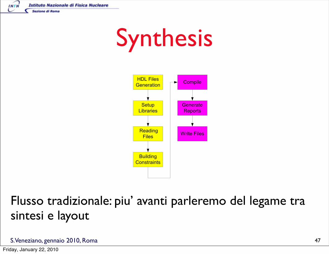
Synthesis
Flusso tradizionale: piu’ avanti parleremo del legame tra sintesi e layout
!
"#$!%&'()
*(+(,-.&/+
0(.12
$&3,-,&()
!4(-5&+6
%&'()
71&'5&+6
8/+).,-&+.)
8/92&'(
*(+(,-.(
4(2/,.)
:,&.(!%&'()
!
!"#$%&'()'*+,"-'./012&,",'!345'
!!
6$"-7'8&9"&5'7(;/,(!5&)<1))&+6!</92&'(=!'(.>)!?1&<@'A!,(B&(C!CD-.!A/1!'(-,+(5!&+!E-,.!FG!!HD(!;&,).!).(2!&)!./!)2(+5!)/9(!.&9(!</''(<.&+6!&+;/,9-.&/+!/+!</5&+6!61&5('&+()!(B(+!&;!A/1!-,(+>.!C,&.&+6!.D(!</5(G!!HD(!,(-)/+!A/1!C-+.!./!5/!.D&)!&)!./!-&5!C&.D!)A+.D()&)!3(<-1)(!.D(,(!-,(!.&9()!CD(+!&.!&)!+(<())-,A!./!,(C,&.(!.D(!</5(G!I+/C&+6!-!;(C!61&5('&+()!<-+!D('2!A/1!-<</92'&)D!.D&)!9/,(!?1&<@'AG!HD(!;/''/C&+6!,()/1,<()!C&''!3(!D('2;1'JG!!
!" $K#L!8/5(!<D(<@(,!!
!" %-.M%,((!"#$!0/'BN(.!-,.&<'(!OPPQQPQ!!
!" 0A+/2)A)!,(;(,(+<(!9-+1-')G!!$&3,-,&()!+((5!./!3(!5(;&+(5!3(;/,(!,(-5&+6!&+!A/1,!</5(G!!HD(!'&+@R'&3,-,A=!.-,6(.R'&3,-,A=!)A93/'R'&3,-,A=!-+5!)A+.D(.&<R'&3,-,A!B-,&-3'()!+((5!./!3(!)(.!./!5(;&+(!A/1,!'&3,-,&()G!!HA2&<-''A!.D()(!B-,&-3'(!5(;&+&.&/+)!-,(!'/<-.(5!&+!A/1,!G)A+/2)A)R5<G)(.12!;&'(G!!S/1!<-+!,(-5!&+!A/1,!</5(!3A!1)&+6!.D(!-+-'AT(U('-3/,-.(!/,!,(-5R;&'(!</99-+5)G!HD()(!</99-+5)!3(D-B(!5&;;(,(+.'A!)/!A/1!)D/1'5!,(B&(C!!
! "
47
Friday, January 22, 2010
S.Veneziano, gennaio 2010, Roma
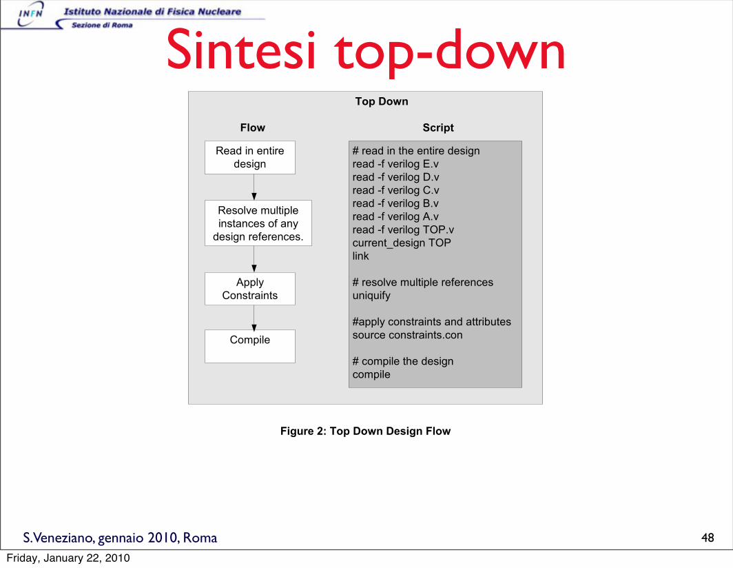
Sintesi top-down!"#$%"&'
!$$$$()"& *+,-#.
"#$%!&'!#'(&)#
%#*&+'
"#*,-.#!/0-(&1-#
&'*($'2#*!,3!$'4
%#*&+'!)#3#)#'2#*5
611-4
7,'*()$&'(*
7,/1&-#
8!)#$%!&'!(9#!#'(&)#!%#*&+'
)#$%!:3!.#)&-,+!;5.
)#$%!:3!.#)&-,+!<5.
)#$%!:3!.#)&-,+!75.
)#$%!:3!.#)&-,+!=5.
)#$%!:3!.#)&-,+!65.
)#$%!:3!.#)&-,+!>?@5.
20))#'(A%#*&+'!>?@
-&'B
8!)#*,-.#!/0-(&1-#!)#3#)#'2#*
0'&C0&34
8$11-4!2,'*()$&'(*!$'%!$(()&D0(#*
*,0)2#!2,'*()$&'(*52,'
8!2,/1&-#!(9#!%#*&+'
2,/1&-#
!
!
(-/0,1$23$!"#$%"&'$%14-/'$()"&$
5".."678#$9"6#-)1$
E,0!*9,0-%!0*#!$!D,((,/:01!$11),$29!3,)!-$)+#)!%#*&+'*5!F#)#!$)#!*,/#!$%.$'($+#*G!!
!" "#C0&)#*!-#**!/#/,)45!!
!" 7,/1&-#*!-$)+#!%#*&+'*!D4!0*&'+!(9#!%&.&%#:$'%:2,'C0#)!$11),$29!!
!" H0&2B-4!&%#'(&3&#*!(9#!2)&(&2$-!1$(9*!3,)!1,**&D-#!)#2,%&'+5!
!
5".."678#$()"&$
6!D,((,/:01!3-,I!)#C0&)#*!$!-,(!/,)#!(&/#!(9$'!$!(,1:%,I'!$11),$295!!F#)#!$)#!(9#!)#C0&)#%!*(#1*J!&'2-0%&'+!*0++#*(#%!*(#1*!(,!3,--,I!&3!(&/&'+!&*!',(!/#(G!!K5! L#'#)$(#!$!%#3$0-(!2,'*()$&'(!3&-#!$'%!*0D%#*&+':*1#2&3&2!2,'*()$&'(!3&-#*5!!>9#!%#3$0-(!2,'*()$&'(!3&-#!*9,0-%!&'2-0%#!+-,D$-!2,'*()$&'(*J!*029!$*!(9#!
! "
48
Friday, January 22, 2010

S.Veneziano, gennaio 2010, Roma
traditional design constraints
• clock definitions
• false paths
• timing checks
49
Friday, January 22, 2010
S.Veneziano, gennaio 2010, Roma
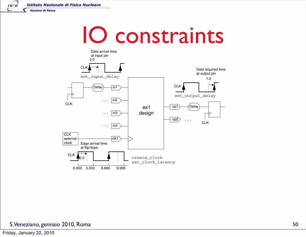
IO constraints
1-10
Chapter 1: Getting Started
The set_output_delay command specifies the amount of
delay from each output to the external device that captures the
output data. It establishes a timing constraint at the outputs and
specifies the required time for output data with respect to the CLK
clock.
Figure 1-3 shows the input and output timing constraints.
Figure 1-3 Input and Output Timing Constraints
clk1
6.6663.3330.000 9.999
create_clock
set_input_delay
set_output_delay
ex1
CLK
CLK
CLK
design
Data arrival time
Data required time
Delay
Delay
...
...
......
in4
in3
in2
in1
op1
op2
CLK
CLK
2.0
1.0
set_clock_latency2.0
Edge arrival time
CLKexternalclock
at input pin
at output pin
at flip-flops
50
Friday, January 22, 2010

S.Veneziano, gennaio 2010, Roma
Clock definitions
51
Friday, January 22, 2010
S.Veneziano, gennaio 2010, Roma
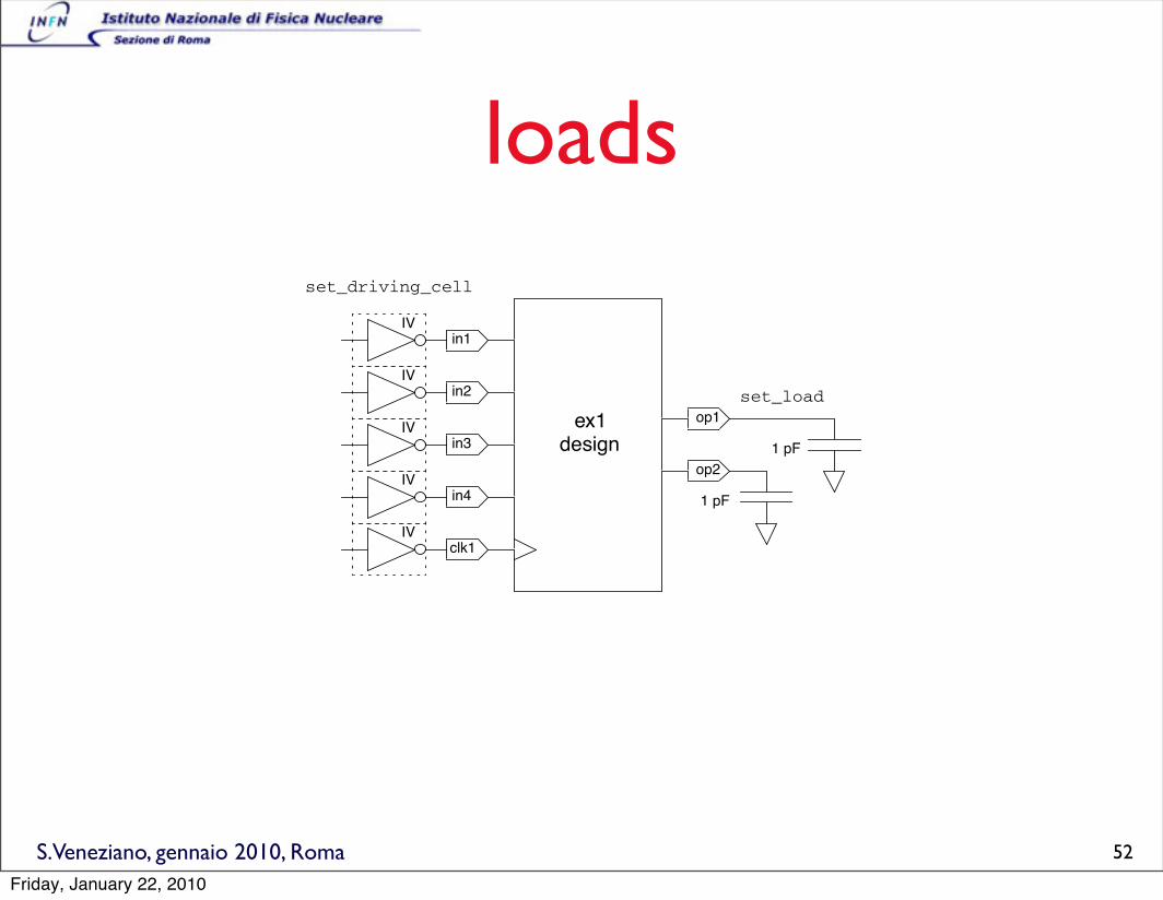
loads
1-12
Chapter 1: Getting Started
2. To specify the capacitive load at the design outputs:
pt_shell> set_load -pin_load 1 [all_outputs]1
The all_outputs command creates a collection of all output
ports of the design. The set_load command sets the external
capacitive load to 1.0 unit for these ports. The units are defined
in the library to be 1 pF.
Figure 1-4 shows the driving cell and loads that have been
specified.
Figure 1-4 Input and Output Timing Constraints
clk1
ex1design
in4
in3
in2
in1
op1
op2
set_driving_cell
IV
set_loadIV
IV
IV
IV
1 pF
1 pF
52
Friday, January 22, 2010
S.Veneziano, gennaio 2010, Roma
timing verification basics
• path delay
• constraints
• analisi
53
Friday, January 22, 2010

S.Veneziano, gennaio 2010, Roma
timing paths
54
Friday, January 22, 2010
S.Veneziano, gennaio 2010, Roma
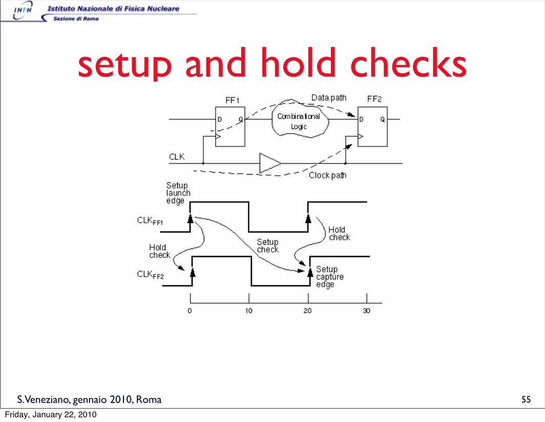
setup and hold checks
55
Friday, January 22, 2010
S.Veneziano, gennaio 2010, Roma
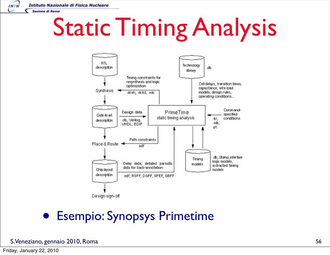
Static Timing Analysis
• Esempio: Synopsys Primetime
56
Friday, January 22, 2010
S.Veneziano, gennaio 2010, Roma
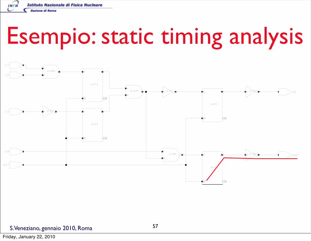
Esempio: static timing analysis
1-4
Chapte
r 1: G
ettin
g S
tarte
d
Figure 1-2Sim
ple Design “ex1_design.v”
57
Friday, January 22, 2010
S.Veneziano, gennaio 2010, Roma
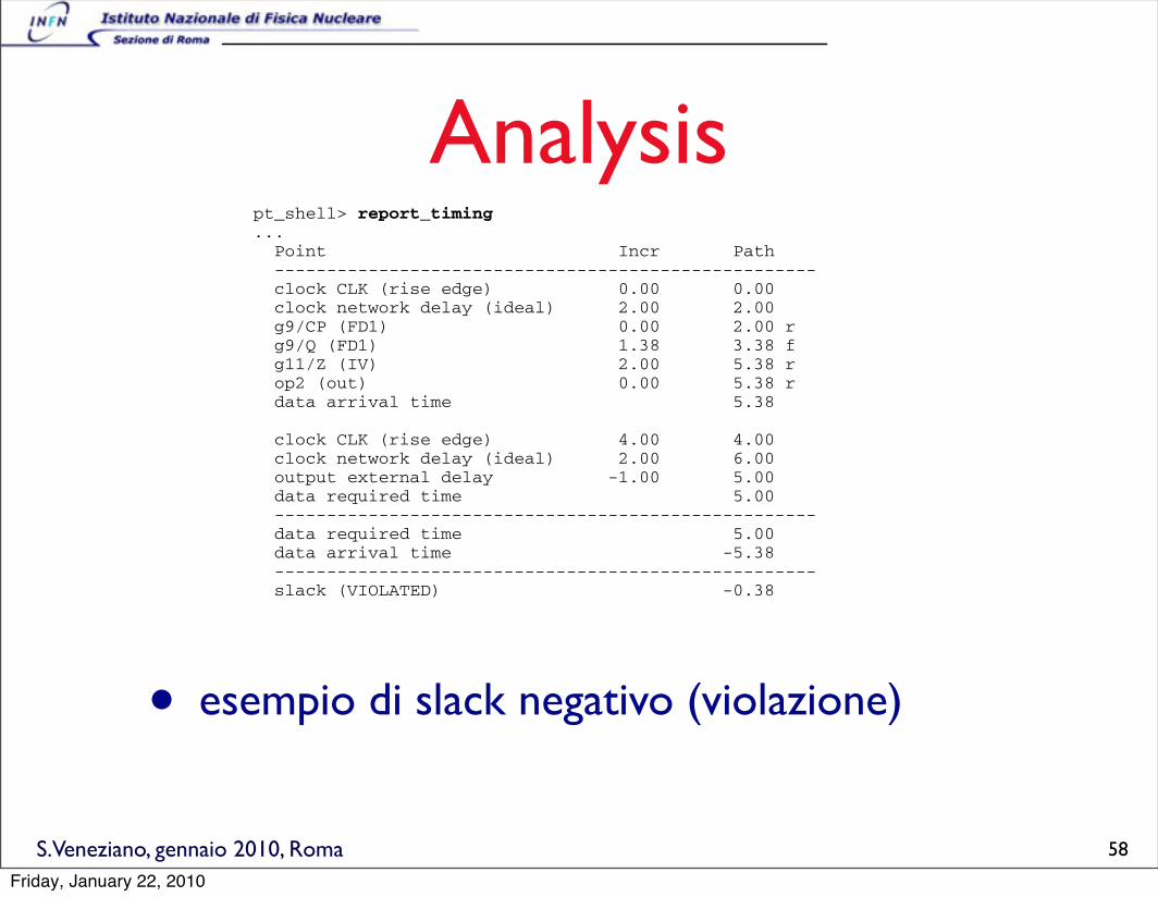
Analysis
• esempio di slack negativo (violazione)1-25
Graphical User Interface
3. Check the clock definition again:
pt_shell> report_clock...Clock Period Waveform Attrs Sources-----------------------------------------------------CLK 4.00 {0 2} {clk1}
The clock period is now 4.00 ns.
Analyze the Design Again
To find out whether the faster clock causes any timing violations, use
the report_timing command.
1. First run the command without any options:
pt_shell> report_timing... Point Incr Path ---------------------------------------------------- clock CLK (rise edge) 0.00 0.00 clock network delay (ideal) 2.00 2.00 g9/CP (FD1) 0.00 2.00 r g9/Q (FD1) 1.38 3.38 f g11/Z (IV) 2.00 5.38 r op2 (out) 0.00 5.38 r data arrival time 5.38
clock CLK (rise edge) 4.00 4.00 clock network delay (ideal) 2.00 6.00 output external delay -1.00 5.00 data required time 5.00 ---------------------------------------------------- data required time 5.00 data arrival time -5.38 ---------------------------------------------------- slack (VIOLATED) -0.38
58
Friday, January 22, 2010

S.Veneziano, gennaio 2010, Roma
Path slacks
1-27
Graphical User Interface
3. In the menu bar of the top-level GUI window, choose Timing >
Histogram > Path Slack. This opens the Path Slack dialog box.
Leave the options at their default settings. Click OK to generate
the histogram.
4. Resize the histogram window and move the vertical pane border
to get the approximate dimensions shown in Figure 1-8. To resize
the window, point to outside border and drag. To move the pane
border, point to it and drag left or right.
Figure 1-8 Path Slack Histogram
The histogram shows the distribution of slack values for different
paths, grouped into eight bins. The red bars represent timing
violations (negative slack values), while the green bars represent
slack values that are not violations (positive slack values).
5. Click the leftmost bar to select it. The selected bar is highlighted
in yellow. The slack values and paths for that bin are listed in the
pane on the right. See Figure 1-9.
Pane border
59
Friday, January 22, 2010
S.Veneziano, gennaio 2010, Roma
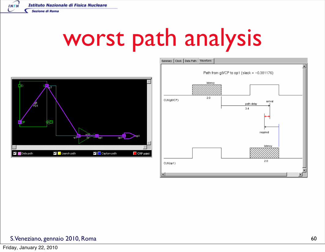
worst path analysis
1-32
Chapter 1: Getting Started
Waveform Viewer
The waveform viewer shows the timing of clock and data transitions
of the path.
1. Click the Waveform tab. This displays the clock waveform for the
path. To make the whole waveform visible, resize the window and
move the border between the waveform and the schematic. See
Figure 1-13.
Figure 1-13 Waveform Display
1-31
Graphical User Interface
Path Schematic
The path schematic shows the cells and nets that are in the path.
See Figure 1-12. The data path starts at flip-flop g8, goes through
inverter g10, and ends at output op1. The purple highlight shows the
data path traversal. You can also highlight the clock launch path and
clock capture path; you will see in later tutorial chapters.
Figure 1-12 Path Schematic
1. Rest the mouse pointer on the wire between the flip-flop and the
inverter. An InfoTip (pop-up text box) shows the net name,
capacitance, and fanout.
2. Rest the mouse pointer on the inverter. An InfoTip shows the cell
instance name, library name, pins, and signal timing.
3. Experiment with the commands in the path inspector’s View
menu and the equivalent toolbar buttons. Try using the scroll bars
at different viewing scales. When you are done, choose View >
Zoom Full.
60
Friday, January 22, 2010

S.Veneziano, gennaio 2010, Roma
Modelli di timing usati
• viene utilizzata l’informazione con il dettaglio disponibile, che aumenta man mano che il progetto cresce:
• pre-layout -> wire loads
• placement -> routing load estimation
• post-route -> detailed parasitics, RC extraction
61
Friday, January 22, 2010

S.Veneziano, gennaio 2010, Roma
Wire loads esempio
• sintesi tradizionale vs sintesi “fisica”.
/* $RCSfile: n18_wc.wireload,v $ *//* $Source: /tmp/covst4386/RCS/n18_wc.wireload,v $ *//* $Date: 2001/05/18 18:19:33 $ *//* $Revision: 1.1 $ *//* *//* ---------------------- *//* Units: Capacitance - pF, Resistance - KOhm, Length - Micron. 1/7/2000 */ wire_load_table ("suggested_default") {/*Eval at 10K gates*/ fanout_length( 1, 8.89 ) ; fanout_length( 2, 20.70 ) ; fanout_length( 3, 31.46 ) ; fanout_length( 4, 38.39 ) ; fanout_length( 5, 62.43 ) ; fanout_length( 6, 68.05 ) ; fanout_length( 7, 95.55 ) ; fanout_length( 16, 520.96 ) ; fanout_length( 32, 732.71 ) ;" fanout_capacitance( 1, 0.0012 ) ;"" fanout_capacitance( 2, 0.0028 ) ;"" fanout_capacitance( 3, 0.0042 ) ;"" fanout_capacitance( 4, 0.0052 ) ;"" fanout_capacitance( 5, 0.0082 ) ;"" fanout_capacitance( 6, 0.0092 ) ;"" fanout_capacitance( 7, 0.0127 ) ;"" fanout_capacitance( 16, 0.0677 ) ;"" fanout_capacitance( 32, 0.0936 ) ;"" fanout_resistance( 1, 0.02120 ) ;" fanout_resistance( 2, 0.04238 ) ;" fanout_resistance( 3, 0.06233 ) ;" fanout_resistance( 4, 0.08017 ) ;" fanout_resistance( 5, 0.11067 ) ;" fanout_resistance( 6, 0.13520 ) ;" fanout_resistance( 7, 0.16679 ) ;" fanout_resistance( 16, 0.51272 ) ;" fanout_resistance( 32, 0.85764 ) ;
wire_load_table ("suggested_20K") { fanout_length( 1, 59.0417 ) ; fanout_length( 2, 75.1218 ) ; fanout_length( 3, 89.7723 ) ; fanout_length( 4, 99.208 ) ; fanout_length( 5, 131.94 ) ; fanout_length( 6, 139.592 ) ; fanout_length( 7, 177.035 ) ; fanout_length( 16, 756.261 ) ; fanout_length( 32, 1044.57 ) ; fanout_capacitance( 1, 0.00763318 ) ; fanout_capacitance( 2, 0.0098117 ) ; fanout_capacitance( 3, 0.0117179 ) ; fanout_capacitance( 4, 0.0130795 ) ; fanout_capacitance( 5, 0.0171642 ) ; fanout_capacitance( 6, 0.0185257 ) ; fanout_capacitance( 7, 0.0232912 ) ; fanout_capacitance( 16, 0.0981776 ) ; fanout_capacitance( 32, 0.133442 ) ; fanout_resistance( 1, 0.0492636 ) ; fanout_resistance( 2, 0.0781016 ) ; fanout_resistance( 3, 0.105265 ) ; fanout_resistance( 4, 0.129555 ) ; fanout_resistance( 5, 0.171083 ) ; fanout_resistance( 6, 0.204482 ) ; fanout_resistance( 7, 0.247494 ) ; fanout_resistance( 16, 0.718502 ) ; fanout_resistance( 32, 1.18814 ) ;
62
Friday, January 22, 2010
S.Veneziano, gennaio 2010, Roma
Sintesi logicaALGORITHMS FOR VLSI DESIGN AUTOMATION
LOGIC SYNTHESIS AND VERIFICATION
1
July 19, 1999
LOGIC SYNTHESIS AND VERIFICATION
Logic synthesis:
* Starts from a register-transfer level (RTL) description, given in e.g.VHDL or given as a set of Boolean expressions.
* Three different tasks: two-level combinational synthesis, multilevelcombinational synthesis and sequential synthesis.
* Outputs a standard-cell netlist or some other form of realization suchas a PLA.
Verification:
* Checks the equivalence of a specification and an implementation.
63
Friday, January 22, 2010
S.Veneziano, gennaio 2010, Roma
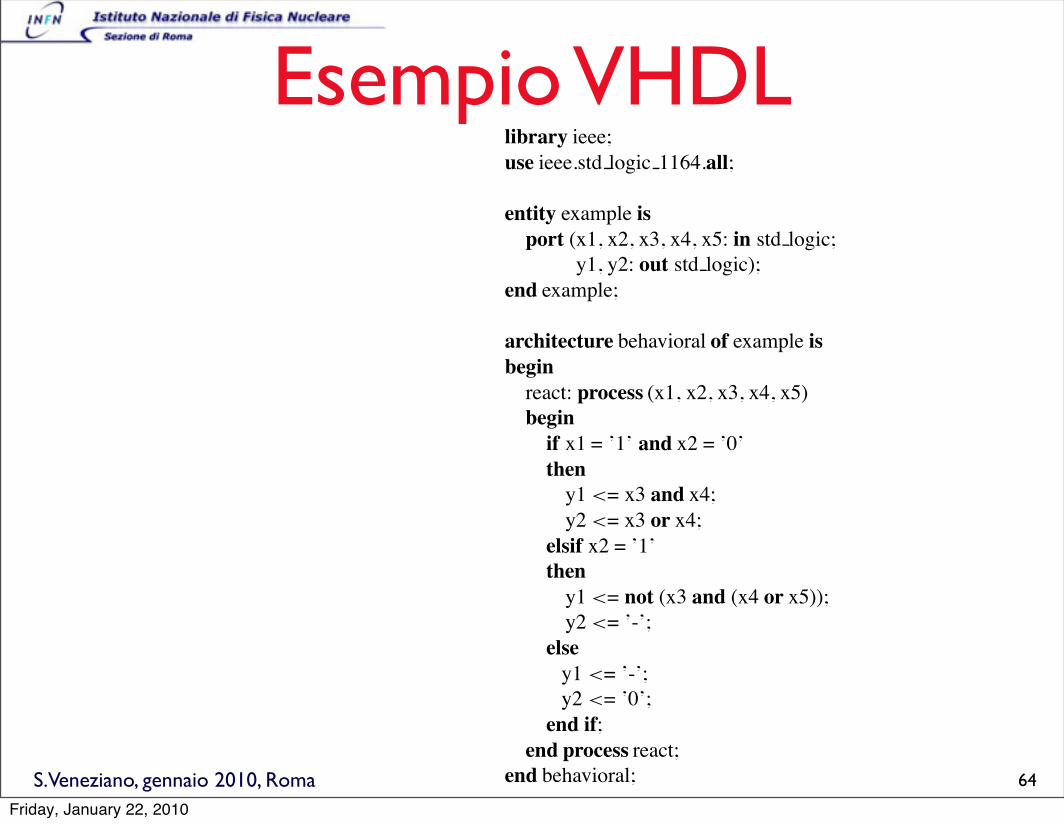
Esempio VHDLlibrary ieee;
use ieee.std logic 1164.all;
entity example is
port (x1, x2, x3, x4, x5: in std logic;
y1, y2: out std logic);
end example;
architecture behavioral of example is
begin
react: process (x1, x2, x3, x4, x5)
begin
if x1 = ’1’ and x2 = ’0’
then
y1<= x3 and x4;
y2<= x3 or x4;
elsif x2 = ’1’
then
y1<= not (x3 and (x4 or x5));
y2<= ’-’;
else
y1 <= ’-’;
y2 <= ’0’;
end if;
end process react;
end behavioral; 64
Friday, January 22, 2010
S.Veneziano, gennaio 2010, Roma
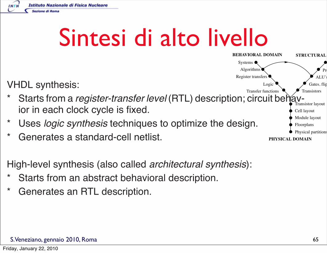
Sintesi di alto livelloALGORITHMS FOR VLSI DESIGN AUTOMATION
HIGH-LEVEL SYNTHESIS
1
June 10, 1999
HIGH-LEVEL SYNTHESIS (HLS)
VHDL synthesis:
* Starts from a register-transfer level (RTL) description; circuit behav-ior in each clock cycle is fixed.
* Uses logic synthesis techniques to optimize the design.
* Generates a standard-cell netlist.
High-level synthesis (also called architectural synthesis):
* Starts from an abstract behavioral description.
* Generates an RTL description.
BEHAVIORAL DOMAIN
PHYSICAL DOMAIN
Physical partitions
Floorplans
Module layout
Cell layout
Transistor layout
Systems
Algorithms
Register transfers
Logic
Transfer functions
Processors
ALU’s, RAM, etc.
Gates, flip-flops, etc.
Transistors
STRUCTURAL DOMAIN
65
Friday, January 22, 2010

S.Veneziano, gennaio 2010, Roma
Modelli hardware
f
i1 i2
o! f (i1, i2)
i1 i2 i3i0
c1
c0
o! ik , k! 2c1" c0
i
o
enable
bus
(a) (b) (c)
(d) (e)
• unita’ funzionali
• registri
• (de)multiplexers
• buses
66
Friday, January 22, 2010
S.Veneziano, gennaio 2010, Roma
Vincoli alla sintesi di alto livello
• ai constraint di sintesi e di timing standard, si aggiungono vincoli sul tipo di unita’ funzionali utilizzabili, sulla possibilita’ di fare pipeline retiming, multicycle operations...
• piu’ in generale sara’ la strategia di clocking, la scelta della connettivita’ (bus vs mux), a determinare l’architettura.
67
Friday, January 22, 2010

S.Veneziano, gennaio 2010, Roma
Esempio di adder
December 12, 2005 Synopsys, Inc. 51
DesignWare IP Family
DW01_addAdder
Arith
DW
L Sythesizable IP
DW01_addAdder
! Parameterized word length
! Carry-in and carry-out signals
! Module Compiler Architectures
Table 1: Pin DescriptionPin Name Width Direction Function
A width bit(s) Input Input dataB width bit(s) Input Input dataCI 1 bit Input Carry-inSUM width bit(s) Output Sum of (A + B + CI)CO 1 bit Output Carry-out
Table 2: Parameter DescriptionParameter Values Description
width !1 Word length of A, B, and SUM
CI
COB
A
SUM
DesignWare IP Family
DW01_addAdder
52 Synopsys, Inc. December 12, 2005
Arith
Table 3: Synthesis Implementationsa
Implementation Name Function License Feature Requiredrpl Ripple-carry synthesis model nonecla Carry-look-ahead synthesis model noneclf Fast carry-look-ahead synthesis model DesignWarebk Brent-Kung architecture synthesis model DesignWare
csmb Conditional-sum synthesis model DesignWare
rpcs Ripple-carry-select architecture DesignWare
clsac MC-inside-DW carry-look-ahead-select DesignWare
csac MC-inside-DW carry-select DesignWare
fastclac MC-inside-DW fast carry-look-ahead DesignWare
pprefixc MC-inside-DW flexible parallel-prefix DesignWare
pparchd Delay-optimized flexible parallel-prefix DesignWare
a. During synthesis, Design Compiler will select the appropriate architecture for your constraints. However, you may force Design Compiler to use one of the architectures described in this table. For more details, please refer to the DesignWare Building Block IP User Guide.
b. The performance of the csm implementation is heavily dependent on the use of a high-performance inverting 2-to-1 multiplexer in the technology library. In such libraries, the csm implementation exhibits a superior area-delay product. Although the csm implementation does not always surpass the delay performance of the clf implementation, it is much lower in area.
c. This architecture is specially generated using Module Compiler technology. It is normally used as a replacement for, rather than in conjunction with, the HDL architectures available for the same DesignWare part. To use this architecture during synthesis, the dc_shell-t variable ‘dw_prefer_mc_inside’ must be set to ‘true.’ From the DC 2004.12 release onward, the MC architectures are not available by default. For more information, refer to the DesignWare Building Block IP Users Guide.
d. This delay-optimized parallel-prefix architecture is generated using Datapath generator technology DW "gensh.” This is ON by default in the Design Compiler flow. The DC variable ‘synlib_enable_dpgen’ must be set to ‘true’ (the default) to make use of this Datapath technology.
68
Friday, January 22, 2010

S.Veneziano, gennaio 2010, Roma
Esempio di sintesi di alto livello// corso master// esempio di codice per sintesi di alto livello//module addera (clk,a,b,d,e,c);input clk;input [7:0] a,b;input [8:0] d,e;output [15:0] c;reg [15:0] c;reg [8:0] banka, bankb;
always @(posedge clk)begin banka <= a + b; bankb <= d - banka; c <= bankb * e;endendmodule
69
Friday, January 22, 2010

S.Veneziano, gennaio 2010, Roma
Esempio di sintesi di alto livello 2
70
Friday, January 22, 2010

S.Veneziano, gennaio 2010, Roma
Mapping
• ...
71
Friday, January 22, 2010

S.Veneziano, gennaio 2010, Roma
floorplan
• ciascun blocco puo’ essere piazzato manualmente, definendone la geometria (area fissa)
72
Friday, January 22, 2010

S.Veneziano, gennaio 2010, Roma
Hierarchy and connectivity
73
Friday, January 22, 2010

S.Veneziano, gennaio 2010, Roma
floorplan
• output: file di floorplan (DEF), piazzamento “hard” di celle di IO e macrocelle, piazzamento “soft” di blocchi di celle standard.
74
Friday, January 22, 2010

S.Veneziano, gennaio 2010, Roma
macrocells placement
75
• in questa fase viene creata anche la rete di distribuzione di potenza (analisi IR dopo il piazzamento).
Friday, January 22, 2010

S.Veneziano, gennaio 2010, Roma
clock tree
• FPGA vs ASIC76
Friday, January 22, 2010

S.Veneziano, gennaio 2010, Roma
clock tree planning and implementation
• sintesi
**** Clock Tree muxb/clockb/U18/Z Stat ****Total Clock Level : 10***** Top Nodes *****muxb/clockb/U18/Z delay[0(ps) 0(ps)] ( muxb/int_clk320__L1_I0/A )Level 10 (Total=9267 Sink=9267)Level 9 (Total=183 Sink=0 CLKBD32=183)Level 8 (Total=24 Sink=0 CLKBD32=24)Level 7 (Total=4 Sink=0 CLKBD32=4)Level 6 (Total=2 Sink=0 CLKBD32=2)Level 5 (Total=1 Sink=0 CLKBD32=1)Level 4 (Total=1 Sink=0 CLKBD20=1)Level 3 (Total=1 Sink=0 CLKBD16=1)Level 2 (Total=1 Sink=0 CLKBD16=1)Level 1 (Total=1 Sink=0 CLKBD16=1)Total Sinks : 9267
********** Clock muxb/clockb/U18/Z Pre-Route Timing Analysis **********Nr. of Subtrees : 1Nr. of Sinks : 9267Nr. of Buffer : 218Nr. of Level (including gates) : 9Max trig. edge delay at sink(R): muxb/coreb/trigb/cm_trig_declu_j0/JREGS/sizeeq34_reg_17_/CK 1887.4(ps)Min trig. edge delay at sink(R): muxb/coreb/trigb/cm_core_slice_1/cm_i_18/j_ge1_16bit_reg_2_/CK 1713.5(ps)
(Actual) (Required) Rise Phase Delay : 1713.5~1887.4(ps) 1720~1720(ps) Fall Phase Delay : 1781.1~1965.6(ps) 1720~1720(ps) Trig. Edge Skew : 173.9(ps) 200(ps) Rise Skew : 173.9(ps) Fall Skew : 184.5(ps) Max. Rise Buffer Tran. : 181.2(ps) 300(ps) Max. Fall Buffer Tran. : 188.2(ps) 300(ps) Max. Rise Sink Tran. : 84.5(ps) 200(ps) Max. Fall Sink Tran. : 78.4(ps) 200(ps)
77
## clk320#AutoCTSRootPin muxb/clockb/U18/ZMinDelay 1720psMaxDelay 1720psSinkMaxTran 200psBufMaxTran 300psMaxSkew 200psBuffer CLKBD2 CLKBD4 CLKBD8 CLKBD12 CLKBD16 CLKBD20 CLKBD32 INVBD2 INVBD4 INVBD8 INVBD12 INVBD16 INVBD20 INVBD32 ExcludedPin+ muxb/clockb/U18/Z#MaxCap#+ CLKBD2 0.13pf#+ CLKBD4 0.13pf#+ CLKBD8 0.13pf#+ CLKBD12 0.13pf#+ CLKBD16 0.13pf#+ CLKBD20 0.13pf#+ CLKBD32 0.13pf#+ INVBD2 0.13pf#+ INVBD4 0.13pf#+ INVBD8 0.13pf#+ INVBD12 0.13pf#+ INVBD16 0.13pf#+ INVBD20 0.13pf#+ INVBD32 0.13pfEnd
Friday, January 22, 2010

S.Veneziano, gennaio 2010, Roma
clock tree skew
78
Friday, January 22, 2010
S.Veneziano, gennaio 2010, Roma
Il piazzamento• E’ il problema di assegnare automaticamente le
posizioni corrette delle celle sul chip, ottimizzando una funzione costo.
• problemi diversi di piazzamento appaiono nel caso di:
• celle standard;
• building blocks;
• celle e building blocks.
• puo’ essere parte integrante del processo di sintesi (sintesi fisica).
79
Friday, January 22, 2010
S.Veneziano, gennaio 2010, Roma
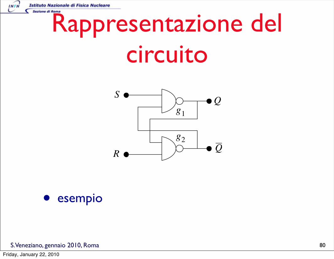
Rappresentazione del circuito
• esempio
S
R
Q
Q
g1
g2
80
Friday, January 22, 2010
S.Veneziano, gennaio 2010, Roma
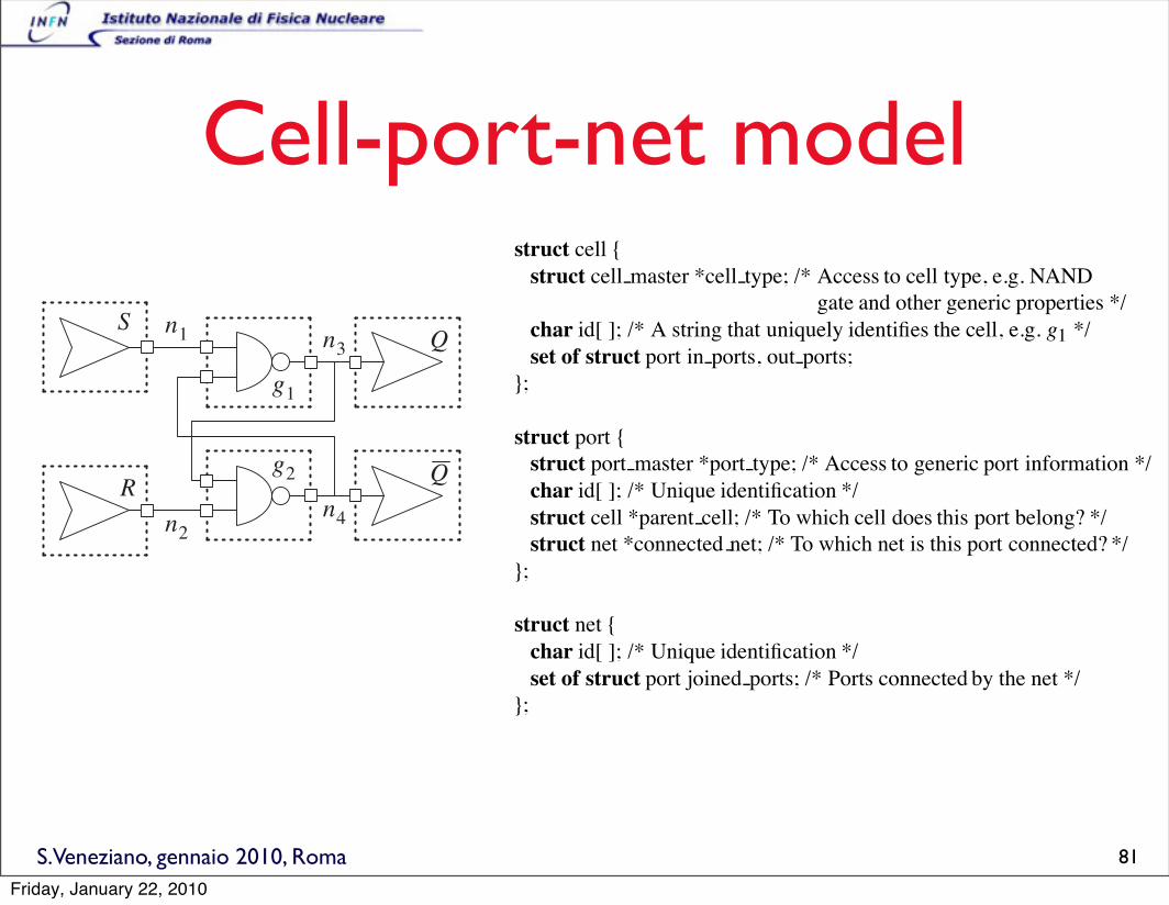
Cell-port-net modelALGORITHMS FOR VLSI DESIGN AUTOMATION
PLACEMENT AND PARTITIONING
2
July 22, 1999
CELL-PORT-NET MODEL
S
R
Q
Q
g1
g2
n1
n2
n3
n4
struct cell {struct cell master *cell type; /* Access to cell type, e.g. NAND
gate and other generic properties */
char id[ ]; /* A string that uniquely identifies the cell, e.g. g1 */
set of struct port in ports, out ports;
};
struct port {struct port master *port type; /* Access to generic port information */
char id[ ]; /* Unique identification */
struct cell *parent cell; /* To which cell does this port belong? */
struct net *connected net; /* To which net is this port connected? */
};
struct net {char id[ ]; /* Unique identification */
set of struct port joined ports; /* Ports connected by the net */
};
81
Friday, January 22, 2010

S.Veneziano, gennaio 2010, Roma
Standard cell
• piazzamento non vincolato.
VDD
GND
CLK
CELL 1 CELL 2
82
Friday, January 22, 2010

S.Veneziano, gennaio 2010, Roma
Relazione col routing• Idealmente, il piazzamento e il routing
dovrebbe essere fatto simultaneamente perche’ ognuno dipende dai risultati dell’altro. Attualmente non e’ possibile fare routing dettagliato e piazzamento con lo stesso tool.
• In pratica il piazzamento viene effettuato in una fase preliminare. Viene fatta una stima delle lunghezze usando una metrica (minimum spanning tree, steiner tree).
83
Friday, January 22, 2010

S.Veneziano, gennaio 2010, Roma
Piazzamento e stima del routing
84
Friday, January 22, 2010

S.Veneziano, gennaio 2010, Roma
Relazione con la sintesi
• wire lenght estimation
• dal floorplan al piazzamento85
Friday, January 22, 2010

S.Veneziano, gennaio 2010, Roma
Routing
• Il routing locale e’ il processo volto a determinare la struttura che connette un insieme di terminali in una data area di routing
• Il routing locale e’ diverso dal routing globale, dedicato all ricerca delle aree di routing dove verranno realizzate le connessioni. Quest’ultimo tipo di routing non fissa le strutture di connessione al’interno delle aree di routing.
86
Friday, January 22, 2010

S.Veneziano, gennaio 2010, Roma
Caratterizzazione• Il routing locale e’ caratterizzato da un numero di parametri (ogni set di
valori definisce un tipo di problema):
• numero di layer di routing
• l’orientazione dei segmenti per ogni layers, orizzontale, verticale, altro
• griglia presente o assente
• presenza o assenza di ostacoli nell’area di routing
• aree di routing fisse o estendibili
• posizione dei terminali: su due linee parallele, su un rettangolo, su un area arbitraria.
• terminali con posizione fissa o mobile.
87
Friday, January 22, 2010

S.Veneziano, gennaio 2010, Roma
Routing all’interno di un blocco di standard cell
• griglia di densita’ di routing, e’ utilizzata anche in fase di piazzamento, per identificare problemi di congestione
(a) (b)
6 (= n)1 2 3 40 5 6 (= n1 2 3 40 5
0
1
2
3
4
5 (= m)
88
Friday, January 22, 2010

S.Veneziano, gennaio 2010, Roma
La sintesi fisica • Procede per fasi (semplificando):
• prima fase di sintesi, senza alcuna informazione fisica. Viene generata la netlist iniziale.
• piazzamento delle celle standard, utilizzando un floorplan (dimensioni die, IO, macrocelle), guidato dai constraints di sintesi (timing-driven)
• iterazione sui due punti seguenti:
• routing approssimato e stima degli RC di ciascuna net
• ottimizzazione delle net piu’ critiche, che violano i constraints di timing/area, attraverso una ottimizzazione logica e il nuovo piazzamento delle celle interessate.
89
Friday, January 22, 2010

S.Veneziano, gennaio 2010, Roma
physical synthesis output
• netlist e piazzamento del circuito, manca il routing dettagliato.90
Friday, January 22, 2010
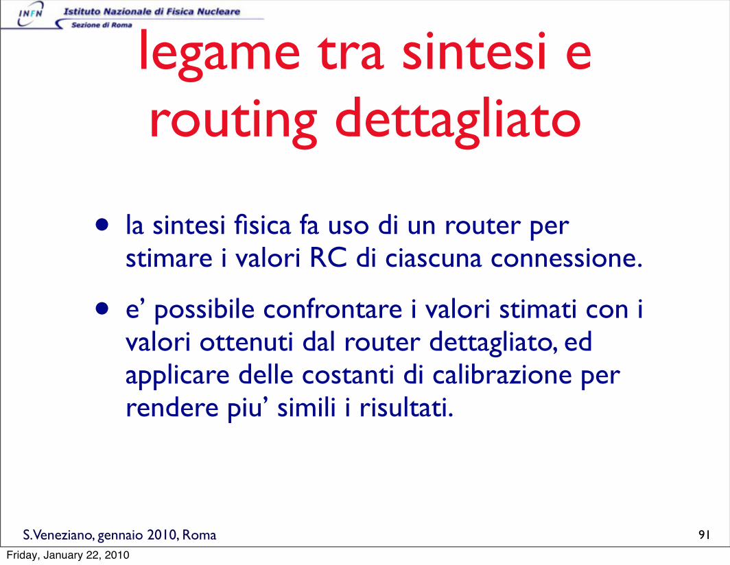
S.Veneziano, gennaio 2010, Roma
legame tra sintesi e routing dettagliato
• la sintesi fisica fa uso di un router per stimare i valori RC di ciascuna connessione.
• e’ possibile confrontare i valori stimati con i valori ottenuti dal router dettagliato, ed applicare delle costanti di calibrazione per rendere piu’ simili i risultati.
91
Friday, January 22, 2010
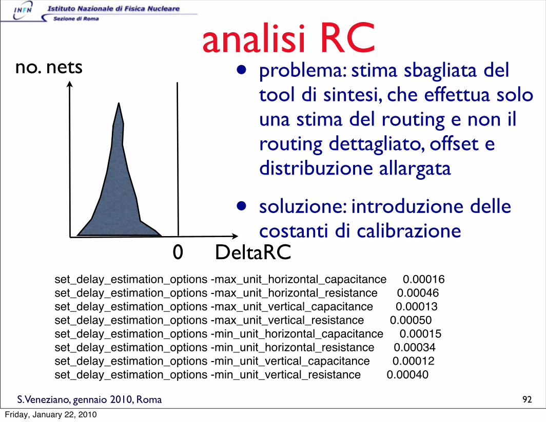
S.Veneziano, gennaio 2010, Roma
analisi RC• problema: stima sbagliata del
tool di sintesi, che effettua solo una stima del routing e non il routing dettagliato, offset e distribuzione allargata
• soluzione: introduzione delle costanti di calibrazione
0
no. nets
DeltaRCset_delay_estimation_options -max_unit_horizontal_capacitance 0.00016set_delay_estimation_options -max_unit_horizontal_resistance 0.00046set_delay_estimation_options -max_unit_vertical_capacitance 0.00013set_delay_estimation_options -max_unit_vertical_resistance 0.00050set_delay_estimation_options -min_unit_horizontal_capacitance 0.00015set_delay_estimation_options -min_unit_horizontal_resistance 0.00034set_delay_estimation_options -min_unit_vertical_capacitance 0.00012set_delay_estimation_options -min_unit_vertical_resistance 0.00040
92
Friday, January 22, 2010

S.Veneziano, gennaio 2010, Roma
Stima e routing finale
• piccole congestioni risolte nella fase di routing dettagliato
93
Friday, January 22, 2010
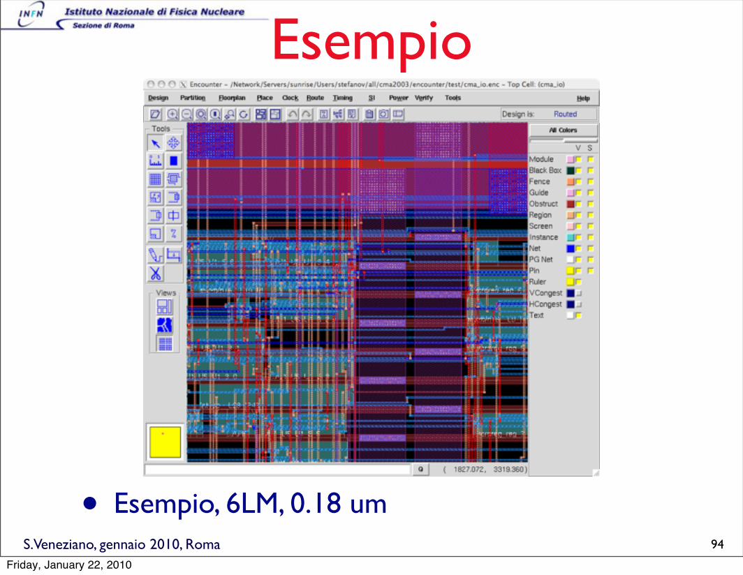
S.Veneziano, gennaio 2010, Roma
Esempio
• Esempio, 6LM, 0.18 um94
Friday, January 22, 2010
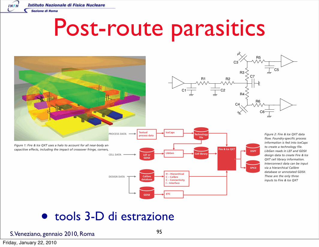
S.Veneziano, gennaio 2010, Roma
Post-route parasitics
• tools 3-D di estrazione
DATASHEET
FIRE & ICE QXTFULL-CHIP 3-D EXTRACTION
Fire & Ice® QXT is a fast, 3-D accurate transistor-level extractor with digital full-chip
capacity. It integrates seamlessly with GDSII and SPICE flows — and with Calibre
through a HCCI interface. Fire & Ice QXT generates parasitic data files in DSPF
and SPICE formats for sign-off timing, power, or signal integrity analysis with
VoltageStorm™ power analysis and CeltIC™ crosstalk analysis.
Figure 1: Fire & Ice QXT uses a halo to account for all near-body and multi-level interconnectcapacitive effects, including the impact of crossover fringe, corners, and capacitive shading
KEY BENEFITS• Transistor-level extraction for final
tapeout verification:
– Extracts data for power grid sign-offwith VoltageStorm
– Device-level and mixed modeextraction
– Integrated with GDSII, LEF/DEFand DEF/GDSII inputs and DSPF,SPICE output
• RC reduction
• Second-generation 3-D adaptiveanalytical extraction modeling
• Distributed, coupled RC data
• Validated in silicon by leading foundries
• Unlimited capacity
SILICON-VALIDATED ACCURACYFire & Ice QXT incorporates an enhancedversion of the production-proven 3-Dadaptive analytical extraction modelingtechnology, which enables distributedand coupled RC extraction faster thanever before. A suite of analyticalmodels is created once per process.
During extraction, parameters aregenerated based on very specific 3-Dregions, then the parameters arepassed to the analytical models forcapacitance calculation. The modelsemploy a special influence region,known as a “dynamic halo.” The halo
accounts for all near-body and multi-level interconnect capacitive effects,including the impact of crossover fringe,corners, and capacitive shading (seeFigure 1). Coupling capacitance playsa dominant role in determining theperformance of UDSM designs, so 3-D
© 2003 Cadence Design Systems, Inc. All rights reserved.Cadence, the Cadence logo, and Fire & Ice are registeredtrademarks and VoltageStorm and CeltIC are trademarksof Cadence Design Systems, Inc. All others are propertiesof their respective holders.
4977 10/03
adaptive analytical modeling extractsboth lumped and fully distributed net-to-net coupled capacitance.
In contrast to less accurate 2-D, 2-D +2-D, or “Quasi 3-D” methods, 3-Dadaptive analytical extraction modelingidentifies in three dimensions all theinteracting objects within the contextof the conductor being evaluated.Because 3-D adaptive analyticalextraction models do not rely onpattern-matching techniques, they donot suffer from boundary errors. 3-Dadaptive analytical extraction modelsscale with shrinking processes andincreasing design sizes and can beused across a broad spectrum ofdesign styles — without “tuning”for each design.
Cadence foundry partners havevalidated the accuracy of 3-D adaptiveanalytical extraction in actual silicon,so users can have confidence that theywill meet their timing budgets anddesign goals. Through the CadenceFoundry Partners program, theseIceCaps models are pre-validated forsix of the world’s leading foundries —Chartered Semiconductor, IBM, NEC,Toshiba, TSMC, and UMC. Models areavailable directly from the foundry.Or you can build your own modelsfor any process technology using thebuilt-in, fully automated IceCapsmodel generation capability inFire & Ice QXT, which makes processtransitions fast and easy (see Figure 2).
3-D ACCURATE EXTRACTIONFire & Ice QXT promotes greater accuracyin timing closure and reduces the
number of layout iterations to achievetargeted design performance. It alsoeliminates the need for excessive over-design in order to meet timing goals.Fire & Ice QXT provides a simplifiedset-up process and single-stepexecution that give designers the fastturnaround and ease of use neededfor transistor-level ASIC design flows.
PERFORMANCE ON 300 MHZ CPUFire & Ice QXT is a transistor-levelextraction product that providesovernight, full-chip, 3-D-accurate,transistor-level extraction for finaltapeout verification. It takes advantageof multiple-CPU processing, by sectioninga design into stripes, then running theresistance and capacitance engines onthe stripes before re-combining thedata to efficiently extract multi-milliontransistor chips. It also extracts the datarequired by VoltageStorm for powergrid sign-off—an essential sign-offrequirement for UDSM designs.
INTEGRATION WITHSTANDARD DESIGN FLOWS
• Fire & Ice QXT includes SPICE andGDSII readers that enable easyintegration with physical design tools
• Produces DSPF and SPICE outputs
• Calibre users can enter design datathrough the HCCI interface (see Figure 2)
• Cadence works closely with EDApartners like Synopsys, Mentor, andMagma to provide support forcommon design flows
PLATFORM SUPPORTFire & Ice runs on standard UNIXworkstations from Sun Microsystemsand Hewlett-Packard.
• OS Support: 32- and 64-bit
• LINUX: Red Hat 7.2 (32-bit)
• Solaris 7 and 8
• HP-UX 11
SYSTEM REQUIREMENTSSystem requirements will vary dependingon your circuit size. Here are somegeneral guidelines:
MINIMUM CONFIGURATION
DRAM: 512 Mb
Swap space: 2 Gb
Disk space for software: 50 Mb
Disk space for 1 million-gate design: 2 Gb
RECOMMENDED CONFIGURATION
DRAM: 1 Gb
Swap space: 4 Gb
Disk space for software: 50 Mb
Disk space for 1 million-gate design: 4 Gb
FOR MORE INFORMATIONLog on to www.cadence.com or emailus at [email protected]
DSPF
Technology file
Cell library
Calibre database
GDSII
LEF or GDSII
SPICE
Fire & Ice QXT
IceCapsTextual process data
PROCESS DATA
CELL DATA
DESIGN DATA
LibGen
XTC
H – HierarchicalC – CalibreC – ConnectivityI – Interface
Figure 2: Fire & Ice QXT dataflow. Foundry-specific processinformation is fed into IceCapsto create a technology file.LibGen reads in LEF and GDSIIdesign data to create Fire & IceQXT cell library information.Interconnect data can be inputvia a hierarchical Calibredatabase or annotated GDSII.These are the only threeinputs to Fire & Ice QXT
7-6
Chapter 7: Parasitic Back-Annotation
Annotating Detailed Parasitics
You can annotate detailed parasitics into PrimeTime and annotate
each physical segment of the routed netlist in the form of resistance
and capacitance (see Figure 7-3). Annotating detailed parasitics is
very accurate but more time-consuming than annotating lumped
parasitics. Because of the potential complexity of the RC network,
PrimeTime takes longer to calculate the pin-to-pin delays in the
netlist.
This RC network is used to compute effective capacitance
(Ceffective), slew, and delays at each subnode of the net.
PrimeTime can read detailed RC in DSPF and SPEF formats.
Figure 7-3 Detailed RC
You can use this model for netlists that have critical timing delays,
such as clock trees. This model can produce more accurate results,
especially in deep submicron designs where net delays are more
significant compared to cell delays.
The detailed RC network supports meshes, as shown in Figure 7-4.
C1
R1
C2
R2
R3
R4
R6
R5
C4
C6
C3
C5
C7
95
Friday, January 22, 2010

S.Veneziano, gennaio 2010, Roma
test vectors generation
• vengono utilizzati strumenti di analisi dei faults.
• passi preliminari necessari in fase di sintesi
96
Friday, January 22, 2010