
UNIVERSITA' DEGLI STUDI DI PADOVApaduaresearch.cab.unipd.it/4024/1/Thesis_PhD_Silvestrin.pdfsistema...
180
1 UNIVERSITA' DEGLI STUDI DI PADOVA TESI DI DOTTORATO Sede Amministrativa: Università degli Studi di Padova Dipartimento di Fisica SCUOLA DI DOTTORATO DI RICERCA IN FISICA INDIRIZZO: ELETTRONICO CIBERNETICO CICLO XXIII Characterization of Electronic Circuits with the SIRAD IEEM: Developments and First Results Direttore della Scuola : Ch.mo Prof. Attilio Stella Supervisore: Ch.mo Prof. Dario Bisello Correlatore: Ch.mo Prof. Jeffery Wyss Dottorando: Luca Silvestrin 31 gennaio 2011
Transcript of UNIVERSITA' DEGLI STUDI DI PADOVApaduaresearch.cab.unipd.it/4024/1/Thesis_PhD_Silvestrin.pdfsistema...

1
UNIVERSITA' DEGLI STUDI DI PADOVA
TESI DI DOTTORATO
Sede Amministrativa: Università degli Studi di Padova
Dipartimento di Fisica
SCUOLA DI DOTTORATO DI RICERCA IN FISICA
INDIRIZZO: ELETTRONICO CIBERNETICO
CICLO XXIII
Characterization of Electronic
Circuits with the SIRAD IEEM:
Developments and First Results
Direttore della Scuola : Ch.mo Prof. Attilio Stella
Supervisore: Ch.mo Prof. Dario Bisello
Correlatore: Ch.mo Prof. Jeffery Wyss
Dottorando: Luca Silvestrin
31 gennaio 2011

2
Introduction
3
Introduction
When an energetic ion strikes a microelectronic device it induces current
transients that may lead to a variety of undesirable Single Event Effects (SEE). An
important part of the activity of the SIRAD heavy ion facility at the 15 MV Tandem
accelerator of the INFN Laboratories of Legnaro (Italy) concerns SEE studies of
microelectronic devices destined for radiation hostile environments.
An axial Ion Electron Emission Microscope (IEEM) is working at the SIRAD
irradiation facility. It is devised to provide a micrometric sensitivity map of Single
Event Effects of an electronic device. The IEEM system reconstructs the positions of
individual random ion impacts over a circular area of 180 µm diameter by imaging
the ion-induced secondary electrons emitted from the target surface. A fast Data
Acquisition system (DAQ) is used to reconstruct the X and Y coordinates and the
temporal information of every ion impact. Any signal induced by the SEE in a
generic DUT can be used to tag the IEEM reconstructed event. This information is
then used to display a map of the regions of the DUT surface which are sensitive to
the impinging ions.
In this thesis we introduce the subject of the effects of ionizing radiation on
microelectronics circuits and systems. We then describe in detail the IEEM system,
especially how it was modified and improved during the period of our work.
We present the results of an extensive study of the IEEM resolution and image
distortions, performed using high statistics acquisitions obtained with a 241 MeV 79Br ion beam by means of a fast SDRAM-based ion induced single event detection
system, specifically designed for this purpose.
We also describe a new feature implemented in the DAQ system which enables
the IEEM to perform Time Resolved Ion Beam Induced Charge Collection
(TRIBICC) studies, and show preliminary results obtained studying a MOSFET
power transistor.

Introduction
4
We also studied a digital microelectronic circuit (SOI-Imager Shift Register) in
two steps: we measured the SEU cross-section with our broad-beam facility at
SIRAD, and then used the IEEM to acquire a SEU sensitivity map.
At present the resolution of the IEEM at SIRAD is not close to the theoretical one.
In this thesis we also describe an extensive set of studies we performed to investigate
the origin of the resolution degradation.
The conclusions follow and close this work.
Introduzione
5
Introduzione
Quando uno ione energetico colpisce un dispositivo microelettronico, induce
impulsi di corrente che possono generare diversi Single Event Effect (SEE)
indesiderati. Una parte importante dell'attività della facility di irraggiamento a ioni
pesanti SIRAD, presso il tandem da 15 MV dei Laboratori Nazionali di Legnaro
(Italia) dell'INFN, riguarda studi di SEE su dispositivi microelettronici destinati ad
ambienti ostili per il livello delle radiazioni.
Presso la facility di irraggiamento SIRAD, e' in funzione un Ion Electron
Emission Microscope (IEEM). Esso e' concepito per generare mappe di sensibilità a
Single Event Effect di un dispositivo elettronico, con risoluzione micrometrica: il
sistema IEEM ricostruisce le posizioni degli impatti di singoli ioni distribuiti
casualmente entro un'area di 180 µm di diametro, acquisendo gli elettroni secondari
emessi dalla superficie del bersaglio colpita dallo ione. Un sistema di acquisizione
veloce (DAQ) è utilizzato per ricostruire le coordinate X ed Y e l'informazione
temporale di ogni impatto. Ogni segnale indotto da un SEE in un generico
dispositivo sotto test può essere utilizzato per marcare gli eventi ricostruiti dal
sistema. Queste informazioni sono in seguito utilizzate per generare una mappa delle
aree della superficie del dispositivo che sono sensibili all'impatto ionico.
In questa tesi introduciamo l'argomento degli effetti della radiazione ionizzante
sui sistemi e i dispositivi microelettronici e in seguito descriviamo in dettaglio il
sistema IEEM, soffermandoci in particolare sulle modifiche e le migliorie introdotte
durante questo periodo di lavoro.
Descriviamo un detector di singoli impatti ionici, basato su una SDRAM, con il
quale abbiamo ottenuto acquisizioni ad alta statistica usando un un fascio di ioni 79Br da 241 MeV. Questi dati ci hanno consentito uno studio approfondito della
risoluzione dell'IEEM e della distorsione dell'immagine generata.
Descriviamo inoltre una nuova caratteristica implementata nel nostro sistema di
acquisizione, che consente all'IEEM di effettuare analisi di Time Resolved Ion Beam

Introduzione
6
Induced Charge Collection (TRIBICC), e illustriamo i risultati preliminari ottenuti
studiando un transistor MOSFET di potenza.
Abbiamo infine studiato un circuito microelettronico digitale (SOI-Imager Shift
Register) in due fasi: dapprima e' stata misurata la sezione d'urto a SEU con la nostra
facility di irraggiamento a fascio non focalizzato, e in seguito l'IEEM e' stato
utilizzato per acquisire una mappa di sensibilità a SEU.
Infine, verificato che allo stato attuale la risoluzione dell'IEEM presso SIRAD non
e' vicina al valore teorico, in questo lavoro di tesi descriviamo la serie di studi
approfonditi condotti al fine di indagare l'origine della degradazione della
risoluzione.

Chapter 1 - Radiation effects on electronic devices
7
1 Radiation effects on electronic devices
The effects of ionizing particles in electronic components are due to the formation
of trails of electron-hole pairs in the semiconductor material along the particle track.
Under the effect of internal or applied electric fields, these charge carriers generate
currents in the external circuit as they move and are collected by electrodes. The
consequences of localized uncontrolled charge injections due, directly or indirectly,
to a single energetic particle have been categorized as Single Event Effects (SEE);
they form a large assortment of anomalies in the operations of many types of devices.
In this chapter I will introduce the subject of radiation effects on electronic
devices and will focus on the physical processes involved in the production of SEE.
1.1 Charge deposition
1.1.1 Introduction
There are two primary methods by which charge is released along the path of an
ionizing particle: direct ionization, due to the coulomb interaction of a charged
incident particle with the electrons of the material, and indirect ionization when the
incident particle interacts (coulomb, nuclear) with the lattice silicon nuclei of the
material to produce secondary ionizing particles (recoils, protons, alphas and other
nuclear fragments).
1.1.2 Direct charge deposition
When an energetic charged particle passes through a semiconductor material, it
frees electron-hole pairs along its path as it loses kinetic energy. When all of its
energy is lost, the particle comes to rest in the semiconductor; the total path length
Chapter 1 - Radiation effects on electronic devices
8
traveled is referred to as the particle’s range. A frequently used quantity is the rate of
energy loss by ionization of the particle, the linear energy transfer (LET):
(2.1) dx
dELET ⋅=
ρ1
with ρ the density of the material and x is the distance along the path of the
particle. The LET is frequently expressed in MeV-cm2/mg. In these units the energy
loss per unit path length (MeV/cm) is normalized by the density of the target material
(mg/cm3), so that the rate of energy loss can be roughly quoted independently of the
target material.
It is easy to relate the LET of a particle to the charge deposition per unit path
length, if one knows the average amount of energy that is needed to create an
electron-hole pair. Consider silicon: the density is 2328 mg/cm3 and approximately
3.6 eV energy deposition is needed to release one electron-hole pair [1], hence a LET
of 97 MeV⋅cm2/mg corresponds to a linear charge deposition of 1 pC/µm. This
conversion factor of about 100 between LET and linear charge deposition in silicon
is handy and should be kept in mind. A useful rule of thumb for silicon is that the
maximum LET of an ion, expressed in MeV-cm2/mg, is roughly equal to its atomic
number Z [2].
The LET is a function of the velocity v of an ion and can be express as:
(2.2) ( ) ( ) ( )vZLETZvZLETQvZLET ,1,1, 222 =××==×= η ,
where LET(Z = 1, v) is the Linear Energy Transfer of a proton with the same
velocity v, and η accounts for the velocity dependence of the effective charge Q = η
× Z of the ion inside the impacted material. The LET(Z = 1, v) of a proton is given
by the Bethe-Boch equation and scales like v-2. The fractional charge η, function of
the atomic number Z of the species and the ion velocity v, can be estimated, within a
few percent, using the parametric form:

Chapter 1 - Radiation effects on electronic devices
9
(2.3)
−×−=
Bethev
vBA exp1η ,
with A = 1 and B ≈ 0.95 [3]. If v >> vBethe the ion is unable to retain electrons and
the charge is the naked nuclear charge Z. As the ion progresses through the material,
it loses energy and slows. When v ≈ vBethe the ion picks up electrons and the effective
charge decreases further as the slowing ion captures more.
The dependence of the LET as a function of the depth reached by the ion slowing
inside a target material is of fundamental interest for understanding the interaction of
a given particle with a device.
Figure 1.1 LET vs ion depth curve for 210MeV 35Cl ion in silicon.
Figure. 1.1 shows the average LET as a function of ion depth for a 210 MeV 35Cl
ion traveling through silicon. A peak in the charge deposition occurs at ∼ 50 µm
below the silicon surface as the particle nears its range. The rate of ionization then
drops as the ion slows and captures more and more electrons, going to zero when the
particle becomes a completely neutral atom. The peak in charge deposition is
referred to as Bragg peak.

Chapter 1 - Radiation effects on electronic devices
10
1.1.3 Indirect charge deposition
Protons and neutrons1 can both produce significant SEE rates due to indirect
mechanism.
As a high energy proton or neutron enters the semiconductor lattice, it may
undergo an inelastic collision with a silicon nucleus. This may result in the emission
of alpha (α) and a recoiling daughter nucleus (e.g. if the Si emits one α-particle, the
recoiling nucleus is Mg), or a spallation reaction, in which the target nucleus is
broken into two recoiling fragments (e.g. Si breaks into C and O ions). These heavy
reaction products deposit large quantities of energy along their paths by direct
ionization, and hence they may induce a SEE. The inelastic collision by-products
typically have low energies and do not travel far from the site of the inelastic
collision of the primary particle. They also tend to be forwarded scattered in the
direction of the primary particle. As a consequence SEE sensitivity is a function of
the angle of incidence of the proton or neutron. Low energy neutrons may also
indirectly create ionizing secondary particles when they interact with the boron used
as a p-type dopant for junction formation in ICs; the isotope 10B is unstable and
neutron capture induces the nucleus to fission into lithium and alpha.
1.2 Charge collection
1.2.1 Introduction
The basic properties of charge collection following a particle strike have been
investigated using several theoretical and experimental methods. The physics of
charge collection have been studied through the use of two and three dimensional
numerical simulations [4][5] or by measuring induced charge collection transients
with ion microbeams and lasers. Ion microbeam and lasers have also been used to
map integrated charge collection as a function of both time and position [6] in ICs.
1 Pions and kaons are hadronic particles which are produced in large numbers in High Energy
Physics experiments at accelerators. Since their effects are very similar to those of protons, they will
not be discussed here.

Chapter 1 - Radiation effects on electronic devices
11
1.2.2 Physics of charge transport
There are essentially three mechanisms that act on the charge carriers deposited
by an ionizing particle:
• carriers can move by drift in response to applied or built-in fields in the
device;
• carriers can move by diffusion under the influence of carrier concentration
gradients within the device;
• carriers can be annihilated by recombination through direct or indirect
processes.
These three mechanisms are of course not unique to the particle strike problem
and are in fact the governing processes of charge transport in semiconductor under
most operating conditions.
When an energetic particle hits a microelectronic device, the most sensitive
regions are reversed biased p/n junctions. In the high field present in the depletion
region of a reversed-biased junction, the charge carriers drift and are efficiently
collected by the electrodes. According to Gunn’s theorem, the drifting carriers induce
a current on electrodes of the device. The induced current appears on an given
electrode delayed only by the time necessary to the electrical field to propagate at the
speed of light the information about the new charge distribution, and not when the
carriers actually reach the electrode. For all practical purposes the signals on all
electrodes appear simultaneously and the induced current will appear on an electrode
even if the carriers do not really reach them, as when recombine or get trapped, etc.
The amount of induced current in the i-th electrode is:
(2.4) i
i V
EqI
∂∂•−=r
rυ ,
where q is the amount of moving charge, Errore. Non si possono creare oggetti
dalla modifica di codici di campo. is the drift velocity, Errore. Non si possono
creare oggetti dalla modifica di codici di campo. is the electrical field at the
position of the charge, Vi is the voltage of the i-th electrode and the derivative is

Chapter 1 - Radiation effects on electronic devices
12
evaluated keeping the potential constant on all other electrodes. The voltage swing
induced by this unwanted current flow can change the logic state of the device,
depending on the amount of the induced charge and on the intrinsic properties of the
circuit to which the device is connected.
Carriers that are produced outside the sensitive depletion region, where the
electrical field is not present, either recombine or diffuse and do not induce a
transient current. The carriers that manage to diffuse into the depletion region do
induce transient currents as they drift and get collected. It is then clear that the
transient induced current will generally have a fast component, due to the prompt
drift of carriers created by a direct particle hit in the sensitive region, and a slow
component, due to the diffusion of carriers created outside the sensitive region that
slowly move into the sensitive region.2
Figure 1.2 Funneling of the junction field to the charge deposited by a ionizing particle.
As a matter of fact, things are a bit more complicated and interesting. Along the
path of a heavily ionizing particle the dense non-equilibrium distribution of electron-
hole pairs induces a funnel-shaped distortion of the potential that extends the electric
field away from the junction and deep into the substrate (Figure. 1.2). This funneling
effect enhances charge collection by drift: charge deposited some distance from the
junction can be collected through the efficient drift process. The prompt (drift)
2 It should be noted that a particle hit near a depletion region can also result in a significant
transient current as carriers diffuse into the depletion region.

Chapter 1 - Radiation effects on electronic devices
13
collection phase typically follows for tens of picoseconds and as the funnel collapses,
diffusion then dominates until all excess carriers have been collected, recombined or
diffused away from the junction area. The current transient typically lasts 200
picoseconds with the bulk of the charge collection occurring within 2÷3 microns of
the junction region for modern submicron CMOS technologies.
1.3 Cumulative effects
1.3.1 Introduction
Energetic particles incident in a solid lose their kinetic energy not only by
producing electron-hole pairs, but also by displacing atoms as they travel through a
given material. Neutrons are particularly good at damaging a silicon lattice. If the
energy of the neutron is sufficient, the primary knock-on atom can also displace
other atoms in the lattice (∼500 for one 1 MeV neutron). For ions the non-ionizing
energy loss (NIEL) is particularly important near the end of range, when the ion is
slow and elastic coulomb collisions with nuclei become important and dominate the
total rate of energy loss (Figure. 1.3).
Figure 1.3 Mean LET and NIEL of a bromine ion in silicon as a function of kinetic energy.

Chapter 1 - Radiation effects on electronic devices
14
In a material like silicon, the accumulation of lattice defects, from the non-
ionizing energy loss of a great number of incident particles, will directly affect the
minority carrier lifetime and mobility, and this lead to modifications of the electrical
characteristics of components (e.g. degradation of electrical parameters; increased
leakage current). The effects of non-ionizing energy loss are categorized as
Displacement Damage Dose (DDD) effects.
When an insulator is exposed to ionizing radiation fixed and charged regions are
induced and the material does not return to its initial state. The homogeneous
accumulation of charge in oxide layers and Si-SiO2 interfaces in silicon devices
exposed to ionizing radiation is at the origin of the parametric degradation of
irradiated devices. These effects are called Total Ionizing Dose (TID) effects.
1.3.2 Displacement Damage
Defect production:
The non-ionizing energy loss produces displaced atoms3. The primary lattice
defects initially created are vacancies and interstitials. A vacancy is the absence of an
atom from its normal lattice position. If the displaced atom moves into a non-lattice
position, the resulting defect is called an interstitial. The combination of a vacancy
and an adjacent interstitial is known as a close pair or Frenkel pair. As regards the
density of defects produced by radiation, at one extreme radiation-induced defects
may be relatively far apart and are referred to as point defects or isolated defects. For
example, incident electrons and photons with energy of the order of 1 MeV produce
such defects. At the other extreme, defects may be produced relatively close together
and form a local region of disorder (defect cluster or disordered region), such as
those ones produced by incident neutrons with energy of the order of 1 MeV, or by a
heavy ions near the end of their range. The mechanism involved is the initial transfer
of a significant amount of energy from the particle to a single Si atom. The dislodged
primary knock-on atom then displaces many other Si atoms locally, thereby creating
a disordered region called a cluster. This may occur several times if the primary
knock-on is energetic enough (Figure. 1.4). In general, incident energetic particles
produce a mixture of isolated and clustered defects. 3 To knock out an atom in Si requires 25 eV.

Chapter 1 - Radiation effects on electronic devices
15
Defect reordering:
Once defects are formed by incident radiation, they will reorder to form more
stable configurations. For example, the vacancy in silicon is an unstable defect and it
is quite mobile at room temperature. After vacancies are introduced, they move
through the lattice and form stable defects such as divacancies (two adjacent
vacancies) and vacancy–impurity complexes. Defect reordering is usually called
annealing and typically implies that the amount of damage and its effectiveness are
reduced (Figure. 1.5). Defect reordering is temperature dependent (thermal
annealing) and dependent on the present excess carrier concentration (injection
annealing). Furthermore, the reordering of defects with time or increased temperature
to more stable configurations can also result in more effective defects, where in this
case the process is often referred in the literature as reverse annealing, in contrast to
the more typical process of forward beneficial annealing.
Figure 1.4 A defect cascade created by a 50 keV primary knock-on silicon ion in silicon.
The primary ion is in red; displaced ions in green. Clusters and super-clusters of displaced
ions are evident (SRIM 2003).

Chapter 1 - Radiation effects on electronic devices
16
Figure 1.5 Conceptual illustration of a short term and long term annealing at room
temperature of displacement damage in bulk silicon and silicon devices [7]
DDD effects:
The discussion on defect reordering clarifies that the effectiveness of radiation-
induced displacement damage depends on the conditions of the irradiation and on the
time passed after irradiation. More generally, damage effectiveness depends on many
factors, including particle type, particle energy, irradiation temperature, measurement
temperature, time after irradiation, thermal history after irradiation, injection level,
material type (n- type or p-type) and impurity type and concentration. The primary
effect of displacement damage that leads to the degradation of material and of device
properties is the introduction of new energy levels in the band gap, associated with
defects (a new energy level arise from a disturbance of lattice periodicity). These
defect states, or centers, have a major impact on the electrical and optical behavior of
semiconductor materials.
Radiation-induced levels in the band-gap can give rise to several processes. Let us
focus, for instance, on the thermal generation of electron-hole pairs through a level
near midgap. This process can be viewed as the thermal excitation of a bound
valence-band electron to the defect center and the subsequent excitation of that
electron to the conduction band, thereby generating a free electron-hole pair. Only
those center near the midgap make a significant contribution to carrier generation4.
4 An exponential decrease in generation rate occurs as the energy-level position is moved from
midgap.

Chapter 1 - Radiation effects on electronic devices
17
Thus, thermal generation of electron-hole pairs (which is the mechanism for leakage
current increases in silicon devices) through radiation-induced defects centers near
midgap is important in device depletion regions.
Another type of effect is the recombination of electron-hole pairs, a process in
which a free carrier of one sign is first captured at the defect center, followed by the
capture of a carrier of the opposite sign. Recombination removes electron-holes pairs
as opposed to the generation process. The mean time a minority carrier spends in its
band before recombining is referred to as the recombination lifetime. Radiation-
induced recombination centers cause the lifetime to decrease: this is the dominant
mechanism for gain degradation due to displacement damage in bipolar transistors.
A third effect is the temporary trapping of carriers at a typically shallow level. In
this process a carrier is captured at a defect center and is later emitted to its band,
with no recombination event taking place. In general, trapping of both majority and
minority carriers can occur (at separate levels). Radiation-induced traps are
responsible for increasing the transfer inefficiency in charge-coupled devices.
A complete review of the literature on the effects of radiation-induced
displacement damage in semiconductors materials and devices can be found in [7].
1.3.3 Total ionization effects
When an MOS transistor is exposed to high-energy ionizing irradiation, electron-
hole pairs are created uniformly along the track of the incident particle throughout
the oxide5. Electron-hole pair generation in the oxide leads to almost all TID effects:
in fact, the generated carriers induce the buildup of charge, which can lead to the
device degradation. The effect of the ionization on MOS devices depends upon the
way that this charge is transported and trapped at the Si-SiO2 interface. The net effect
of ionizing radiation on MOS device oxides depends upon the oxide thickness, the
field applied to the oxide during and after exposure, as well as trapping and
recombination within the oxide. The manufacturing processing techniques strongly
affect the latter factor.
After pair creation, in general, some of electrons will recombine with holes
(depending on the material, the kind of radiation and the applied field, which acts 5 In oxide (SiO2), the electron-hole pair creation energy is ∼ 17 eV.
Chapter 1 - Radiation effects on electronic devices
18
separating the pairs). Following the initial creation process, the radiation-generated
electrons and holes are transported under the applied electric field. Most of the
electrons will drift in picoseconds toward the gate, where they are collected, while
holes, far less mobile in Si than electrons6, linger where they have been generated.
After this, the holes undergo a “hopping” transport over the Si/SiO2 interface,
through localized states in oxide. As the holes approaches the interface, some
fraction (strongly depending on the process) of the holes will be trapped, forming a
positive oxide trap charge. Most of the holes are trapped within 7 nm of Si/SiO2
interface and generally anneal with time.
In addition to hole trapping and annealing at the Si/SiO2 interface, there is build
up of radiation-induced interface traps. Hydrogen ions (protons) are likely to be
released as holes “hop” through the oxide or as they are trapped near the Si/SiO2
interface. The protons can drift to the Si/SiO2 interface where they may react to form
interface traps. In addition to oxide-trapped charge and interface-trap charge buildup
in gate oxides, charge buildup will also occur in other oxides including field oxides
and silicon-on-insulator (SOI) buried oxides.
Semi-permanent TID effects in MOS devices and circuits caused by the buildup
of space charge in the SiO2 layer fall into several categories, such as voltage offsets,
or shifts, induced parasitic leakage currents and mobility degradation.
In general, the effect of radiation-generated charge ∆ρ on the threshold voltage
shift ∆Vth of a transistor is given by:
(2.5) ( ) ( )( )dxtxxCV ox
t
oxth
ox
∫ ∆−=∆0
1 ρ ,
where tox is the oxide thickness, Cox is the oxide capacitance and x is measured
from the gate-SiO2 interface. From equation (1.6) it can be seen that positive charge
(trapped holes) will cause a negative shift in the threshold voltage of a device, while
negative charge will cause a positive shift in the threshold voltage. In general, the
initial response of an MOS transistor to radiation is a negative shift in the threshold
voltage, due to buildup of trapped holes. For a sufficiently large amount of trapped
positive charge, the n-channel device may be turned on even for a zero applied gate
6 In Silicon: µelectrons ≤ 0.14 m2/V·s, µholes ≤ 0.05 m2/V·s.

Chapter 1 - Radiation effects on electronic devices
19
bias. In this case the device is said to have gone into “depletion mode”. When
strongly into depletion, the n-channel device ceases to function because it cannot be
switched from the ON to the OFF state: it is always ON (Figure. 1.6)!
Figure 1.6 Schematic cross section of an MOS transistor illustrating charge buildup in the
gate oxide
Charge gathered in the thick field oxide will also turn on a parasitic leakage path
at the edges of the gate metal, where current can flow from source to drain outside
the channel region. The irradiation-induced shift of the gate-oxide curve is small due
to the thin thickness of gate oxide layer. On the contrary, while the contribution of
the field oxide leakage current is negligible before irradiation, after irradiation it
becomes the major effect. This is due to the larger thickness of the field oxide respect
to the gate one, this resulting in a larger voltage shift per unit dose. The combination
of two effects makes the leakage current raise several orders of magnitude after
irradiation, which is often enough to cause functional failure of the devices.
Figure 1.7 shows the voltage threshold shift effect for a typical commercial
process. Hardened devices will exhibit much lower threshold shifts primarily because
of recombination in the oxide. Present commercial CMOS technologies will usually
fail at levels between 10 and 50 krad(Si). To set the scale, the total dose that can be
accumulated during 10 years in space may range from a minimum of a few krad(Si)
and may reach up to 100 krad(Si).7 The total dose that will accumulated in 10 years
7 In SiO2 the number density of electron-hole pairs per unit dose is n = 7.6×10¹² e-h/cm3-rad; in Si
n = 3.7×10¹³ e-h/cm3-rad.

Chapter 1 - Radiation effects on electronic devices
20
by the frontend electronics of the silicon CMS tracker at LHC will range from
100krad(Si) to 50 Mrad(Si).
Figure 1.7 Voltage shift due to irradiation.
Chapter 2 - Single Event Effects
21
2 Single Event Effects
Single Event Effects (SEE), as the name suggests, are due to the interaction of a
single particle with a semiconductor device. In this chapter I will discuss SEE and
describe the various types of effects that can be induced by a single particle strike.
2.1 Introduction
2.1.1 Brief history of SEEs
The first confirmed report of cosmic-ray-induced Single Event Upsets (SEU,
discussed later) in space was presented at the NSREC8 in 1975 by Binder et al.[8]. In
this paper, four upsets in 17 years of satellite operation were observed in bipolar J–K
flip–flops operating in a communications satellite. The authors used scanning
electron microscope (SEM) exposures to determine the sensitive transistors and,
using a diffusion model, calculated a predicted upset rate within a factor of two of
the observed rate. Due to the small number of observed errors, the importance of
SEU was not fully recognized until 1978–1979, when significant numbers of SEU-
related papers were presented at the NSREC.
The occurrence of soft errors in terrestrial microelectronics manifested itself
shortly after the first observations of SEU in space [9]. This watershed paper from
authors at Intel found a significant error rate in DRAMs as integration density
increased to 16 to 64K. The primary cause of soft errors at ground level was quickly
diagnosed as due to alpha particle contaminants in the package materials.
Radioactive contaminants in the water used by the factory were contaminating the
ceramic packages of devices.
8 NSREC: Nuclear and Space Radiation Effect Conference.
Chapter 2 - Single Event Effects
22
In the late 1970s, evidence continued to mount that cosmic-ray-induced upsets
were indeed responsible for errors observed in satellite memory subsystems, and the
first models for predicting system error rates were formulated [10]. By this time
satellite memory systems had increased in size and on-orbit error rates of one per day
could not be ignored.
Even though the first papers attributed memory upsets to direct ionization by
heavy ions, by 1979 two groups reported at the NSREC on errors caused by proton
and neutron indirect ionization effects [11] [12]. This was a very important
discovery, because of the much higher abundance of protons relative to heavy ions in
the natural space environment: not only would SEE be caused by galactic cosmic
rays, but also by protons trapped in the Earth’s radiation belts and by solar event
protons. The paper by Guenzer et al.[12] was the first to use the term “single-event
upset”, and this term was immediately adopted by the community to describe upsets
caused by both direct and indirect ionization. The year 1979 also brought the first
report of single-event latchup (SEL, described later), an important discovery given
the potentially destructive nature of the failure mode.
In the early 1980s, research on SEU continued to increase and methods for
hardening ICs to SEU were widely developed and used throughout this decade [13]
[14]. There were also few studies on another emerging and potentially troubling
single-event issue: errors due to single events in combinational or imbedded logic.
The 1990s saw two major developments that continued to increase the importance
of SEEs. One was the dramatic decrease in the number of manufacturers offering
radiation-hardened digital ICs. This (among other factors, such as the increased
functionality and performances they could provide) led to the increased usage of
commercial electronics in spacecraft systems. However, their relative sensitivity to
SEE presented significant challenges to maintaining system reliability. The second
development was the continued advance in fabrication technologies toward smaller
IC feature sizes and the higher speeds and more complex circuitry that scaling
enables. These advances typically increase sensitivity to SEE, even to the point of
errors occurring in a benign desktop terrestrial environment, and may also lead to
new failure mechanisms. These two developments led to an interesting convergence
of mission from two historically disparate communities: space and military vendors

Chapter 2 - Single Event Effects
23
driven toward commercial (non radiation hardened) circuits and commercial vendors
driven toward a very real concern about SEE in the everyday consumer environment.
As we enter the 21st century, concern about sensitivity to SEU is expected to
continue, both in memories and core logic. Upsets in terrestrial electronics are a
serious reliability concern for commercial manufacturers. At the same time,
feasibility of traditional SEU-hardening techniques is becoming questionable,
especially because of fewer dedicated rad-hard foundries implementing them. Circuit
design that are inherently radiation resistant (Hardening By Design, HBD) are
receiving considerable attention [15] [16].
2.1.2 Classification of SEE
In Chapter 1 we have seen how an ion strike releases charge along its path
through a semiconductor and how this charge can be collected by p/n junctions, but
what really matters is determining whether the event actually causes an error in
circuit operation. In the following sections we will study how charge collection
interacts with the circuit type and design to create a single-event effect. Here we
report the major types of single event phenomena, which can be classified into
several categories:
• Single event upset (soft error that can be reset)
• Single event latchup (soft or hard errors)
• Single event burnout (hard failures)
• Single event gate rupture (hard failures)
2.2 Single Event Upset
2.2.1 Introduction
Single event upset, or SEU, is the most common type of single event effect. SEU
is caused by the deposition of charge in a device by a single particle, that is sufficient
to change the logic state of a single bit (from one binary state to another). Whether or
Chapter 2 - Single Event Effects
24
not the charge deposited through direct ionization is sufficient to cause an upset of
course depends on the type of device and circuit that has been struck, as well as the
strike location and particle trajectory. Direct ionization is the primary charge
deposition mechanism for upsets caused by heavy ions (ions with atomic number Z ≥
2, i.e. He and above). Lighter particles, such as protons, do not usually produce
enough charge by direct ionization to cause upset in memory circuits, but researches
have suggested that single event effects due to direct ionization by protons may occur
in new and more susceptible ICs [17] [18].
Single bit upsets are sometimes called soft errors because a reset or a rewriting of
the device results in normal device behavior thereafter. An SEU may occur in analog,
digital, or optical components; it may also have effects in surrounding interface
circuitry to which they are connected, but this strongly depends on the nature of the
interconnections. Some memory devices are also susceptible to Multiple Bit Upset
(MBU), in which more than one bit is upset. This can be caused by a single ion
traveling essentially parallel to the die surface, depositing energy in the sensitive
volume of a consecutive line of memory cells, or striking the die close to normal,
depositing enough energy in two or three adjacent cells to upset them. A severe SEU
is the Single-Event Functional Interrupt (SEFI) in which an SEU in the control
circuitry of the device places it into a test mode, halt, or undefined state. The SEFI
halts normal operations, and requires a power reset to recover.
In the next paragraphs the focus will primarily be on memory circuits, as this will
be the main field of application of the equipment described in this thesis.
2.2.2 Single Event Upset in DRAM
SEUs in terrestrial electronics were first observed in DRAMs [9] [19]. This kind
of memories have historically been quite susceptible to soft errors because they rely
on passive storage of charge to represent information: there is no inherent refreshing
of this charge packet (e.g., charge resupply through a load device) and no active
regenerative feedback. Their charge state is readily modified by funnel-assisted drift
or diffusion following an energetic particle strike; they hence allow any disturbance,
no matter how small, of the stored information to persist, until corrected by external
circuitry.

Chapter 2 - Single Event Effects
25
What is so often referred to as a bit flip, the transition from one stable binary state
to the other, is not required in DRAMs for an SEU to occur. A degradation of the
stored signal to a level outside the noise margin of the supporting circuitry is
sufficient to lead to erroneous interpretation and a resultant error. DRAMs have
therefore received less use in space systems as engineers have preferred SRAM
technologies. As the need for very large amounts of on-board memory is increasing,
the use of DRAM technologies in space systems is becoming more common.
DRAMs are prone to SEU due to three primary mechanisms: storage cell errors,
bit-line errors and a combination of the two.
Figure 2.1 illustrates the mechanism for storage cell errors in a field plate
capacitor DRAM [20]. In this kind of DRAM a stored “0” is represented by electrons
occupying a potential well under the field plate, while a stored “1” corresponds to
electrons being depleted under the plate. Following a particle strike, electrons can be
collected at the reverse-biased field plate. In the case of a stored “0”, this just
reinforces the original state, but a stored “1” can look like a stored “0” after electron
collection.
Figure 2.1 Illustration of storage cell SEU in a field-plate DRAM. Collections of electron
at the reverse-biased field plate reinforces a stored “0”, but can lead to an upset of a stored
“1”.
Upsets can also occur in DRAMs due to bit-line strikes. When the bit lines are in
a floating voltage state (e.g. during a read cycle), DRAMs are sensitive to the
collection of charge into diffusion regions that are electrically connected to the bit
access lines.9 The bit-line error is the reduction of the sensing signal due to a charge
imbalance introduced of the precharged bit lines. Because they can only occur during
9 This collection could arise from any of the access-transistor drains along the floating bit-line or
from a direct strike to the sense amplifier circuitry itself.

Chapter 2 - Single Event Effects
26
a read cycle, bit-line errors have a direct dependency on the read access frequency,
with an increasing error rate as the access frequency increases.
A new failure mode for DRAMs was demonstrated when it was found that charge
collection at both the storage cell and bit line, that was insufficient to individually
cause an upset, could cause an error in combination [21]. This new failure mode,
dubbed the Combined Cell-Bit line (CCB) error, was shown to dominate the storage
cell and bit-line error rates for very short cycle times. The three components of soft
errors in a 512K DRAM are shown in Figure. 2.2 as a function of the cycle time.
Note the independence of storage-cell errors on cycle time, and the domination of
CCB errors for short cycle times.
Figure 2.2 Components of soft-error rate in DRAM [21]. The storage cell component is not
dependent on the cycle time, while soft errors involving the bit lines increase dramatically as
the cycle time decreases.
2.2.3 Single Event Upset in SRAM
The upset process in SRAMs is quite different from DRAMs, due to the active
feedback in the cross-coupled inverter pair that forms a typical SRAM memory cell,
as illustrated in Figure. 2.3. When an energetic particle hits a sensitive location in a
SRAM (typically the reverse-biased drain junction of a transistor biased in the “off”
state, T1 in figure), charge collected by the junction induces a transient current in the
struck transistor. As this current flows through the struck transistor, the restoring
transistor (“on” p-channel transistor, T2 in figure) sources current in an attempt to

Chapter 2 - Single Event Effects
27
balance the particle-induced current. The current flowing through the restoring
transistor, due to the finite transistor channel conductance, induces a voltage drop at
its drain (point A in Figure. 2.3). This voltage transient (in response to the single-
event current transient) is actually the mechanism that can cause upset in SRAM
cells. In fact, T2 drain is also connected to the gates of transistors T3 and T4. If the
induced current is sufficient to lower the voltage of restoring transistor drain below a
threshold voltage, the logical states of T3 and T4 will be inverted. This will
consequently force the voltage of point B to go to VD (it was at zero before the hit),
so switching T1 and T2 and changing the state of the cell as a result. Competition
between the feedback process and the recovery process governs the SEU response of
SRAM cells. In fact, if the recovery current sourced by the restoring transistor is
faster than the feedback one, the circuit will not flip, although the induced transient
current is obviously still present.
Figure 2.3 Schematic layout of a CMOS SRAM cell.
Interestingly, even incident particles with LET far below the upset threshold are
often sufficiently ionizing to induce a momentary voltage “flip” at the struck node of
an SRAM (Figure. 2.4). Whether an observable SEU occurs depends on what
happens faster: the feedback of the voltage transient through the opposite inverter, or
the recovery of the struck node voltage as the single-event current dies out. It must
be noted that drift (including funneling effects) is responsible for the rapid initial flip
of the cell, while long-term charge collection by diffusion prolongs the recovery
process; both mechanisms are critical to the upset process.

Chapter 2 - Single Event Effects
28
Figure 2.4 SRAM struck drain voltage transient for ion strikes with LET well below, just
below and just above the SEU threshold.
The recovery time of an SRAM cell to a particle strike depends on many factors,
such as the particle LET, the strike location, etc. From a technology standpoint, the
recovery time depends on the restoring transistor current drive and minority carrier
lifetimes in the substrate [22] [23]. A higher restoring current leads to a fast recovery
time, as do decreased minority carrier lifetimes10. The cell feedback time is simply
the time required for the disturbed node voltage to feed back through the cross-
coupled inverters and latch the struck device in its disturbed state. This time is
related to the cell write time and in its simplest form can be thought of as the RC
delay in the inverter pair. This RC time constant is thus a critical parameter for
determining SEU sensitivity in SRAMs: the smaller the RC delay, the faster the cell
can respond to voltage transients (including write pulses) and the more susceptible
the SRAM is to SEUs. Obviously this has implications for the sensitivity of future,
higher speed technologies.
2.2.4 Single Event Upset in SOI devices
Due to their intrinsic structure, Silicon On Insulator (SOI) devices were regarded
to be much less sensitive to upsets than conventional bulk silicon circuits. In a bulk
Si transistor the charge generated by an ion strike is fully collected from the substrate
10 This is because a higher restoring current is more quickly able to re-establish the struck node
voltage, while decreased substrate minority carrier lifetimes reduce the diffusion current at the struck
node.

Chapter 2 - Single Event Effects
29
region, regardless whether the gate or the drain has been hit. In a SOI transistor,
instead, (see Figure. 2.5) the volume area sensible to charge collection is made
smaller by the buried oxide that prevents charge deposited in the substrate to be
efficiently collected. However, it has been shown how it is possible to have charge
collection from below the buried oxide in SOI technologies that use a very thin
buried (on the order of 200 nm) oxide layer [24].
For these technologies it has been measured that the saturated cross section (~ 8
µm2/bit) was closer to the sum of the active gate and drain areas (6.1 µm2/bit) rather
than to the gate area alone (0.64 µm2/bit). This indicates that, contrary to the earlier
beliefs, charge collection could also occur from the substrate below the buried oxide,
at least in some SOI technologies.
From past studies, it is known that charge collection occurs only when the
substrate is biased in depletion or inversion mode, and the mechanism for charge
collection at top electrode was assumed to be due to a capacitive discharge or to a
displacement current. Recent studies and simulations [25] with dedicated microscopy
experiments performed at microbeam facilities, led to a deeper understanding of this
kind of phenomenon.
Figure 2.5 Charge collection behavior in SOI transistor
2.2.5 Single Event Upset in logic circuits
Although we have concentrated on SEU in memory circuits, they can also occur
in other digital circuits, prime examples being microprocessors and digital signal
processors. Errors in logic circuits are very sensitive to critical timing windows and
logic paths, and may never propagate to the output pins. Therefore, in core logic, the

Chapter 2 - Single Event Effects
30
concepts of “faults” and “errors” are distinct from memory circuits and require
precise definition.
In a logic circuit, charge collection due to a single-event strike on a particular
node will generate a low-to-high or high-to-low voltage transition or a transient noise
pulse. If this pulse is larger than the input noise margin of a subsequent gate, it will
compete with the legitimate digital pulses propagating through the circuit. The ability
of the noise pulse to propagate depends not only on its magnitude, but also on several
more factors. First, the existence of active combinational paths from the struck nodes
to latches11; second, the arrival time of the erroneous signal at the latches; third, the
erroneous pulse time profile at the latch input12. If all three of the above conditions
are properly met, then the SE-generated noise pulse will be captured by the latch as
erroneous information. We define this as the generation of a soft fault (SF).
SFs may also be generated by direct single-event strikes to the latch nodes, where
the latch information is corrupted via a bit flip. In this case the effect is analogous to
SEUs in memory circuits and can be modeled in a similar way.
Once a SF has been identified, or a SF probability has been calculated, one knows
the vulnerability of a circuit to single events and/or critical paths which may
contribute a weak link for single-event tolerance. However, actual upset rates, which
refer to the observable operation of a particular circuit located in a particular hostile
radiation environment, cannot be immediately deduced from knowledge of SFs.
Internal SFs may not be observable at the interface pins of a circuit (or the I/O ports
of a subcircuit). For example, the particular latch effected by the soft fault may be
part of a “don’t care” state of the finite state machine; the change of state has no
effect on subsequent operation of the circuit. Or, the erroneous latch data may be part
of a data register that is scrubbed in a subsequent clock cycle. Thus, no observable
error actually occurs. However, if the soft fault eventually propagates to one or more
of the I/O ports of the circuit, then an externally observed error exists; we define this
and only this event as an error event. It is clear that one soft fault may cause
11 The active combinational paths depend on the dynamic state of the logic as determined by the
particular code vectors executed at that time (the present “state” of the logic). 12 The pulse must arrive within the setup and hold (S/H) time of the latch element to be stored by
the latch element. The clocking characteristics of the latch and the previous state of the latch
contribute to this mechanism.

Chapter 2 - Single Event Effects
31
erroneous information at many I/O ports and that this erroneous information may
appear during many clock cycles.
2.2.6 Single Event Upset in analog circuits
SEU can occur in almost any integrated circuit. For example, SEU is not
constrained to digital circuits, but also occur in analog circuit as well.
Upsets in photodiodes used in optocoupler applications have been observed and
correlated to direct ionization by protons. Single-Event current Transients (SET)
resulting from proton direct ionization are capable of causing upsets in these
photodiodes because they are by design very large and operate at very high data
rates. A recent analysis suggests that a combination of direct ionization and recoils
are responsible for the anomalous angular dependence of proton upsets in
optocouplers. Charge-coupled devices (CCDs) can also be sensitive to direct
ionization by protons because of their large collection depths [26].
Errors are observed in many analog circuit types, including operational amplifiers,
comparators, analog-to-digital converters (ADCs). Upsets in ADCs are interesting
because analog errors are observed as corruptions in digital output codes.
2.3 Other kinds of SEE
2.3.1 Single Event Latchup (SEL)
Circuits are made by combining adjacent p-type and n-type materials into
transistors. Paths other than those chosen to form the desired transistor can
sometimes result in so-called parasitic transistors, which, under normal conditions,
cannot be activated. A latchup is the inadvertent creation of a low-impedance path
between the power supply rails of an electronic component, triggering the above
mentioned parasitic structure, which then acts as a short circuit, disrupting proper
functioning of the part and possibly even leading to its destruction due to
overcurrent. A power cycle is required to correct this situation.
The parasitic structure is usually an equivalent of a thyristor (or Silicon Controlled
Rectifier, SRC), a PNPN structure which acts as a PNP and an NPN transistor

Chapter 2 - Single Event Effects
32
stacked next to each other (Figure. 2.6). During a latchup, when one of the transistors
is conducting, the other one begins conducting too.
Figure 2.6 Lateral section of a p/n/p/n structure with two parasitic BJTs
They both keep each other in saturation for as long as the structure is forward-
biased and some current flows through it (it usually means until a power-down). The
SCR parasitic structure is formed as a part of the totem-pole PMOS and NMOS
transistor pair on the output drivers of the gates.
2.3.2 Single Event Gate Rupture (SEGR)
Dielectric breakdown can occur when the electric field across an insulating
material exceeds some threshold value. When initiated by an energetic particle strike
to the gate region of an MOS device, this phenomenon is referred to as a Single-
Event Gate Rupture (SEGR).
Single-event gate rupture has been studied most extensively for power devices
such as double-diffused power MOSFETs (DMOS), so we will use this device or
describing the SEGR mechanism.
As shown in Figure. 2.7, current flow in the DMOS structure is vertical rather
than lateral as in a standard MOSFET. Application of a positive bias to the gate in
this n-channel DMOSFET inverts the p-body region to form a channel between the
n-source at the top of the structure and the drain (substrate) contact at the bottom of
the structure. To handle large currents, the full structure usually contains hundreds or
thousands of these cells connected in parallel.

Chapter 2 - Single Event Effects
33
Figure 2.7 Structure of a vertical power MOSFET and current flow paths following a
heavy ion strike.
The thick lightly-doped epitaxial region allows the power MOSFET to sustain high
voltages without breakdown. When an ion strikes the neck region through the gate
oxide, SEGR can occur as charge is transported near the Si/SiO2 interface. As charge
from the ion strike accumulates underneath the gate region (and depending on the
gate bias), the electric field in the gate insulator can temporarily increase to above the
critical field for breakdown, causing a localized dielectric failure (i.e., an SEGR).
The SEGR response in vertical power MOSFETs has two components [27]. The
“capacitor response” describes the interaction of the ion directly with the gate
dielectric, inducing an oxide breakdown at a lower field than would occur in the
absence of the ion strike. If a drain bias is applied when the ion strike occurs, part of
the drain voltage may be transferred through the epitaxial layer to the gate interface
[28]. This part of the response is referred to as the “substrate response.” Increasing
the gate voltage increases susceptibility to SEGR through the capacitor response by
increasing the pre-existing electric field in the oxide. Increasing the drain voltage
also increases the susceptibility to SEGR because part of this voltage can be coupled
to the interface through the substrate response.
SEGR effects have been studied for some time in power devices, but a topic that
has recently received a considerable amount interest is SEGR in logic and memory
ICs. As gate oxide thicknesses decrease, SEGR could become a problem in ICs
because they will likely be operated at somewhat higher electric fields.
Chapter 2 - Single Event Effects
34
2.3.3 Single Event Burnout (SEB)
Single Event Burnout (SEB) due to heavy ions, neutrons and protons has been
observed both in power MOSFET and in bipolar transistor. SEB is a destructive
failure mechanism that comes about due to a parasitic bipolar transistor structure
inherent to some devices. Looking at the power MOSFET structure in Figure.2.7, a
parasitic bipolar transistor is formed by the n-source (emitter), p-body (base) and n-
epitaxial (collector) regions. Following an ion strike, currents flowing in the p-body
can forward bias the emitter-base junction of the parasitic BJT due to the finite
conductivity of the p-body region. The parasitic BJT is now operating in the forward
active regime, and if the drain-to-source voltage is higher than the breakdown
voltage (BVCEO) of the parasitic BJT, avalanche multiplication of the BJT collector
current can occur. If this positive feedback (regenerative) current is not limited, it can
lead to junction heating and the eventual burnout of the device [29].
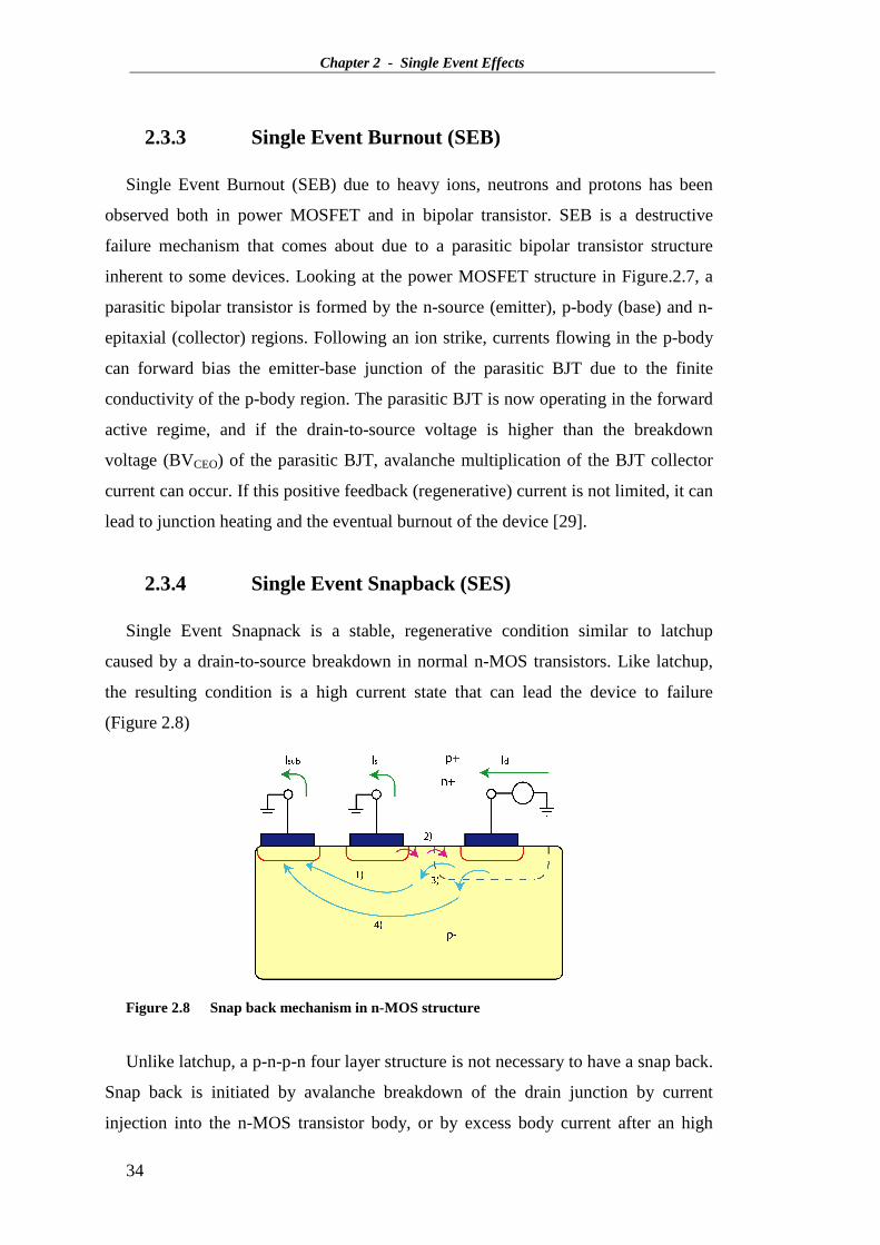
2.3.4 Single Event Snapback (SES)
Single Event Snapnack is a stable, regenerative condition similar to latchup
caused by a drain-to-source breakdown in normal n-MOS transistors. Like latchup,
the resulting condition is a high current state that can lead the device to failure
(Figure 2.8)
Figure 2.8 Snap back mechanism in n-MOS structure
Unlike latchup, a p-n-p-n four layer structure is not necessary to have a snap back.
Snap back is initiated by avalanche breakdown of the drain junction by current
injection into the n-MOS transistor body, or by excess body current after an high

Chapter 2 - Single Event Effects
35
dose rate radiation pulse or an heavy ion strike. After an ion hit, excess current near
the drain junction results in avalanche multiplication and injection of holes that flow
in the body region to the body contact (1) and cause the potential at the source-body
junction to increase. If an avalanche condition is sustained long enough due to a
sufficiently large current pulse, the source-substrate junction becomes forward biased
turning on the parasitic npn bipolar transistor and injecting electrons into the
substrate (2). As these feed into the drain, additional avalanche multiplication occurs
(3), causing an increased substrate current and completing the regenerative feedback
mechanism (4). Snap back cannot be triggered unless an external circuit provides
sufficient current; for this reason, it is usual observed onto I/O stages of ICs equipped
with large current drive pull up transistors. It is not observed in p-channel devices
because the ionization rate for holes is much lower than for electrons, and
regenerative feedback is consequently much lower.
2.4 The SIRAD Single Events irradiation facility
2.4.1 Introduction
The SIRAD heavy ion irradiation facility, located at the 15 MV Tandem-XTU
accelerator at the INFN National Laboratory of Legnaro (Italy) is dedicated to
radiation damage studies in silicon detectors and devices. An important part of the
experimental program is the study of ion induced SEE in microelectronic devices and
systems. Devices under test are exposed to a broad beam (few cm2) and global
characterizations are routinely performed. A wide selection of swift ion species, from
Li to Au, is available to test most modern technology electronic devices for high
energy physics and space applications. The IEEM discussed in this work was non-
invasively installed to extend SEE capabilities of the SIRAD beam-line to include
the ability to reconstruct the impact points of individual ions with high resolution. In
this section we will give a detailed description of SIRAD facility.
Chapter 2 - Single Event Effects
36
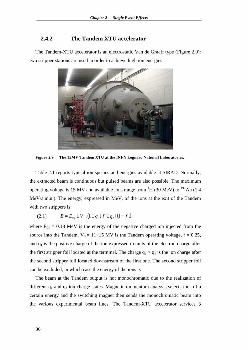
2.4.2 The Tandem XTU accelerator
The Tandem-XTU accelerator is an electrostatic Van de Graaff type (Figure 2.9):
two stripper stations are used in order to achieve high ion energies.
Figure 2.9 The 15MV Tandem XTU at the INFN Legnaro National Laboratories.
Table 2.1 reports typical ion species and energies available at SIRAD. Normally,
the extracted beam is continuous but pulsed beams are also possible. The maximum
operating voltage is 15 MV and available ions range from 1H (30 MeV) to 197Au (1.4
MeV/a.m.u.). The energy, expressed in MeV, of the ions at the exit of the Tandem
with two strippers is:
(2.1) ( )( )fqfqVEE inj −⋅+⋅+⋅+= 11 210
where EInj = 0.18 MeV is the energy of the negative charged ion injected from the
source into the Tandem, V0 = 11÷15 MV is the Tandem operating voltage, f = 0.25,
and q1 is the positive charge of the ion expressed in units of the electron charge after
the first stripper foil located at the terminal. The charge q2 > q1 is the ion charge after
the second stripper foil located downstream of the first one. The second stripper foil
can be excluded, in which case the energy of the ions is
The beam at the Tandem output is not monochromatic due to the realization of
different q1 and q2 ion charge states. Magnetic momentum analysis selects ions of a
certain energy and the switching magnet then sends the monochromatic beam into
the various experimental beam lines. The Tandem-XTU accelerator services 3

Chapter 2 - Single Event Effects
37
experimental halls and 10 beam lines: the SIRAD beam line is the +70° in the
heavily shielded hall 1 ( Figure 2.10)
(2.2) ( )10 1 qVEE inj +⋅+=
Figure 2.10 Picture of the SIRAD irradiation facility at INFN Laboratori Nazionali di
Legnaro. The large global irradiation chamber in foreground is open. The IEEM chamber is
downstream and not visible.
2.4.3 The SIRAD irradiation facility
Bulk damage and SEE studies are routinely addressed at the SIRAD irradiation
facility of the INFN National Laboratory of Legnaro (Padova, Italy) by Universities
and Industrial groups, involved in the study of the radiation hardness of
semiconductor devices and electronic systems for high energy physics and space
applications [60].
The characteristics of the typical ion beams available at the SIRAD irradiation
facility are reported in Table 4.1: the energy values refer to the most probable q1 and
q2 charge state, obtained with two stripper stations and with the Tandem operating at

Chapter 2 - Single Event Effects
38
14 MV; the surface ion LET0 and range reported are for silicon (calculated by
SRIM).
Ion Energy (MeV) q1 q2 LET0 (MeV × cm2/µg) Range (µm) 1H 28 1 1 0.02 4390 7Li 56 3 3 0.37 378 11B 80 4 5 1.01 195 12C 94 5 6 1.49 171 16O 108 6 7 2.84 109 19F 122 7 8 3.87 99.3 28Si 157 8 11 8.59 61.5 32S 171 9 12 10.1 54.4
35Cl 171 9 12 12.5 49.1 48Ti 196 10 14 19.8 39.3 51V 196 10 14 21.4 37.1 58Ni 220 11 16 28.4 33.7 63Cu 220 11 16 30.5 33.0 74Ge 231 11 17 35.1 31.8 79Br 241 11 18 38.6 31.3
107Ag 266 12 20 54.7 27.6 127I 276 12 21 61.8 27.9
197Au2 275 13 26 81.7 23.4
Table 2.1 Characteristics of the typical ion beams available at the SIRAD irradiation
facility with the Tandem operating at 14 MV. The values of the LET0 and the range are for
silicon.
At present when using 197Au beams in SIRAD the operating voltage is typically
lowered to 11.6 MV due to a temporary limitation in the maximum current in the
power supply of the switching magnet that deviates the beam into the line at 70°.13
The ion species reported in Table 4.1 have been selected in order to minimize the
time required for the ion source change during SEE tests. When possible two multi-
sources (the first including O, Si, Ni and Ag; the second including F, Cl, Br, and I)
are used to decrease the time for beam setting.
The essential elements of the SIRAD line, shown in Figure 2.11, are:
• a system of adjustable horizontal and vertical slits;
13 We plan to remove all limitations of this type by stripping further electrons from the ions just
before the analyzing magnet.

Chapter 2 - Single Event Effects
39
• a quadrupole doublet for focusing the beam down to millimetric spots;
• an electric rastering system for irradiating extended targets;
• an irradiation chamber with a vertical sample-holder, available both for
diagnostic and irradiation purpose;
• a chamber with an extractable Faraday cup (FC70);
• an irradiation chamber including a battery of small Faraday cups and a
battery of silicon PIN diodes with pulse counting electronics.
Figure 2.11 Schematic drawing of the SIRAD irradiation facility. The IEEM chamber is
downstream of the large global irradiation chamber (SIRAD chamber). A smaller chamber
upstream is used for beam diagnostics.
The typical spot size diameter of a focused beam is 3-4 mm and beam diagnostics
is performed by an extractable Faraday Cup positioned in a diagnostic chamber
located ∼ 1 m upstream of the target plane. Visual inspection of the beam profile may
be performed on a quartz window positioned at the end of the irradiation chamber.

Chapter 2 - Single Event Effects
40
An image intensifier is sometimes used to see the beam spot on the quartz for
tenuous beam current.
In order to irradiate a large target with a focused proton or ion beam, a rastering
system is used. The system, produced by IBA (Louvain-la-Neuve, Belgium), is made
of vertical and horizontal deflection plates 1 m long, with 5 cm gaps, and with
linearly ramped voltages (Vmax = ±15 kV) at slightly different frequencies (νx = 625
Hz, νy = 612 Hz). The rastering system permits a uniform irradiation (better than 5%)
over a fiducial area of 5×5 cm2 on the target plane. On-line monitoring of the beam
current and uniformity on the target is provided by a square battery of 3×3 small
Faraday cups, located behind the target plane (sample holder). This configuration is
suitable for radiation tests at beam currents higher than 100 pA/cm2 and is currently
used for proton induced bulk damage studies in silicon.
The very low ion fluxes (102-105 ions/(cm2⋅s)) necessary for global SEE studies in
electronic devices and systems are obtained by closing machine collimators to
achieve low beam currents (< 1 nA) and by defocusing the beam on the target plane
by adjusting the SIRAD quadrupole doublet (see Figure 2.11). The doublet is
positioned before the rastering system, which is normally not used in SEE
experiments (it is used instead for high current bulk damage studies or intense ion
beam irradiation). The ion fluxes for SEE tests are well below the sensitivity of the
Faraday cups and the beam spot cannot be seen with the quartz system. To setup the
beam, measure the ion flux, uniformity and the quality of the beam (mono-
chromaticity) we use an array of silicon PIN diodes as particles counters in the target
plane. During irradiation the device under test is surrounded by 4 diodes and the
beam characteristics are monitored.
The same beam-set up procedure is used when the IEEM is used. A single PIN
diode inside the IEEM chamber is used to measure the ion flux and the beam quality.

Chapter 3 - SEE studies
41
3 SEE studies
3.1 SEEs modeling
3.1.1 Introduction
Modeling Single Event Effect rates in a microelectronic device involves a
combination of:
• assumptions about the physics of the device;
• detailed knowledge of the radiation environment;
• real experimental.
The device physics that underlies SEE involves charge generation along the path
of a primary or secondary ionizing particle, charge transport and collection on circuit
nodes and the final response of the circuit to the charge transient. Both the total
collected charge and the rate of charge collection can be important to triggering a
single event effect. Models that predict SEE rates typically use test data obtained at
accelerator irradiation facilities to extract information about the device sensitivity.
The typical information sought for are the cross section σ and the critical charge
(QC), as a function of LET or the energy of the incident particles. The experimentally
measured cross section for a device can be expressed as the ratio between the number
of SEE counted for a certain fluence of particles of a given LET or energy:
(3.1) [ ]2cmfluence
counts=σ .
Once the cross section versus the particle LET or energy has been measured, there
are established techniques for using the data to predict SEE rates in a given radiation

Chapter 3 - SEE studies
42
environment. The rate prediction methods do a fairly good job of predicting what is
actually observed in a radiation hostile environment, such as onboard a spacecraft.
As a first approximation the occurrence of SEEs is driven by the quantity of
deposited energy. This allows one to reduce all particle types and energy
distributions present in the radiation environment to their LET and to calculate the
deposited energy by integrating the LET along the trajectories throughout the
sensitive volume. With this simplification, the problem is to define the size of the
sensitive volume, calculate the rate of particle hits and the consequent energy
depositions, and determine the fraction of total particle hits that cause SEEs. The
SEE rate is the product of the sensitive area on the chip by the flux of particles in the
environment that can cause the considered event. The problem is complicated by the
angular dependence since the amount of energy deposited in the sensitive volume
depends on chord length, which in turn depends on angle of incidence of the striking
particle.
This model was first proposed by Pickel and Blandford in 1978 [30] and was later
implemented in several simulation codes. This method models the sensitive volume
as a right rectangular parallelepiped (RRP) with lateral dimensions x and y and
thickness z (Figure 3.1). The ion path through the RRP is s and is determined by
thickness, z, and the angle of incidence, θ, between the xy plane. Charge is also
allowed to be collected along a funneling distance, sf, that adds to s for the charge
calculation.
The energy deposited in the sensitive volume from an ion interaction with LET, L,
is
(3.2) ( )LssE f+≈ .

Chapter 3 - SEE studies
43
Figure 3.1 Schematic of the RPP model parameters
This energy is converted to ionization charge and it is assumed that all the charge
generated within the charge collection length s+sf is collected by the sensitive
volume circuit node. This model is also based on the following assumptions: ion
plasma track structure can be ignored, ion LET is constant along a chord s through
the sensitive volume, charge collection by diffusion from ion strikes external to the
RRP can be ignored and there is a sharp threshold for upset, i.e. ions with a LET
below threshold will not cause SEEs, ions with a LET above the threshold will
always give SEEs.
To get a SEE rate R(EC) prediction, the model integrates the LET distribution and
the expected ion flux over the chord-length modulated by an analytic differential
distribution f(S) function relation:
(3.3) ( ) ( ) ( )[ ]( )dssfEsLAER
zyx
ctpc ∫++
Φ=21222
0, .
where the integration goes from zero to the maximum path-length through the
RPP, Ap is the average projected area of the RPP, Φ(L) is the integral flux, Ec is the
threshold energy for generating Qc and Lt(s, Ec) is the minimum average LET
depending on chord length through

Chapter 3 - SEE studies
44
(3.4) ( )f
cct ss
EEsL
+=, .
As already mentioned above, the RPP model assumes a step function for cross
section versus LET value. However, most devices show a gradual rise from threshold
to saturation, rather than a step function. This behavior is due to the superposition of
composite response of multiple types of sensitive volumes, with different thresholds
and with distribution of their parameters. To solve this issue, it has been proposed
[31] to divide the cross-section curve into several steps in order to more accurately
represent it. The generally accepted approach is to integrate in energy and weigh
with the normalized experimental cross-section data
(3.5) ( ) ( )∫=sat
c
E
E
dEEfERR .
where the integration range is from the measured threshold, Ec, to the measured
value at saturation, Esat, and f(E) is the cross-section versus LET curve converted to a
probability density, described by the four parameter Weibull distribution:
(3.6) ( ) ,exp1
−−−=S
c
W
EEEf .
where EC is the threshold energy, while W and S are two shape parameters used to
fit the curve to the experimental data. The f(E) function represents the rate at which
an energy of E is deposited in the sensitive volume. It can be regarded as the
probability density for an event caused by deposition of an energy quantity equal or
greater than E. This approach is commonly called the integral RPP (IRPP).
3.1.2 Prediction for proton-induced SEU
Only the most sensitive devices (such as high density DRAMs and CCDs) are
sensitive to SEU from the direct ionization of a proton because the proton LET is so
low. However, protons can cause SEU through nuclear reactions14, which result in
14 With nuclear reactions we mean both coulomb plus strong interactions with nuclei.
Chapter 3 - SEE studies
45
recoiling ions that can deposit enough energy in the sensitive volume to cause upsets
even in less sensitive devices such as SRAMs.
To get reliable proton induced SEE predictions the key step is to determine the
energy spectra of the ion recoils as a function of the material and the incoming
proton energy; the knowledge of the energy distribution of the recoil products will
then allow to estimate SEE rates following the heavy ion model. The model shown
here [32] has been derived by observing how proton SEU cross-section data (as a
function of proton energy) follow a relationship resembling the proton nuclear cross
section in silicon. The Bendel parameter, A, was introduced on a semi-empirical
basis; the original formulation had both a threshold and a limiting cross section but
the single parameter A was adequate to describe the data available at the time. As
more data became available, it became clear that the response of some modern
smaller feature size devices was better modeled with the use of both parameters. An
improved two-parameter Bendel model was suggested by two groups at about the
same time, and this is the form that currently has the widest acceptance [33] [34].
The two-parameter model is expressed as
(3.7) ( )[ ]45.014
18.0exp1 YA
Bp −−
=σ .
where σp is a cross section in units of 1012 upsets per proton/cm2 per bit, A and B
are empirically determined constants unique to a device and
(3.8) ( )AEA
Y −= 18.
with E as proton energy in units of MeV.
The parameter A is related to the apparent upset energy threshold, while the ratio
( )14AB is associated with the saturation cross section observed at high energies. The
one-parameter model has B fixed at a value of 24. The advantage of the two-
parameter model is that it allows better fitting of the experimental data in the high
energy regions, particularly for small geometry devices, while preserving the
apparent low energy proton upset threshold. Also for protons, a closer fit matching
can be obtained by the superimposition of Weibull’s distribution curves with

Chapter 3 - SEE studies
46
different fixed parameters. The important thing to notice here is that, in contrast with
heavy ions case, the proton upset rate depends on the probability of a nuclear
interaction to happen within the whole device size, and not only during the path of
the proton in the device active volume.
3.2 Test with accelerators
3.2.1 Introduction
The final goal of this thesis is to describe a new tool to measure the SEE
sensitivity of electronic devices to ionizing radiation. In this chapter we will give a
review of the traditional methods employed to perform this kind of measurement,
underlining the strong and the weak aspects of currently adopted techniques.
3.2.2 Laboratory accelerator based measurements
The essential part of any SEE qualification process is actually performing test
measurements: electronic devices undergo radiation tests to check their behavior
under controlled conditions that well reproduce the environment where they are
expected to work in. Simulation tools derived from first principles are certainly
useful in providing some indication of SEE device sensitivity of a particular type of
device, but reliable predictions of actual performances may not be made without real
data, possibly collected with the very same type of device.
The radiation environment in space is widely varied in composition, energy,
orbital position, time, and it is largely omni-directional. To validate a component or
device for use in the space environment, irradiation facilities at particle accelerators
are routinely used to test the SEE sensitivity of electronic components in controlled
and repeatable conditions. A broad variety of ion species, with adequate energies, are
required to perform reliable tests.
The energy of a certain type of particle delivered by an accelerator sets the LET
(Linear Energy Transfer) and the range; i.e. the depth the particle will travel inside
the target. Of course the LET of a particle varies with energy and hence it changes
along the particle trajectory as the particle slows. As already mentioned, the LET is
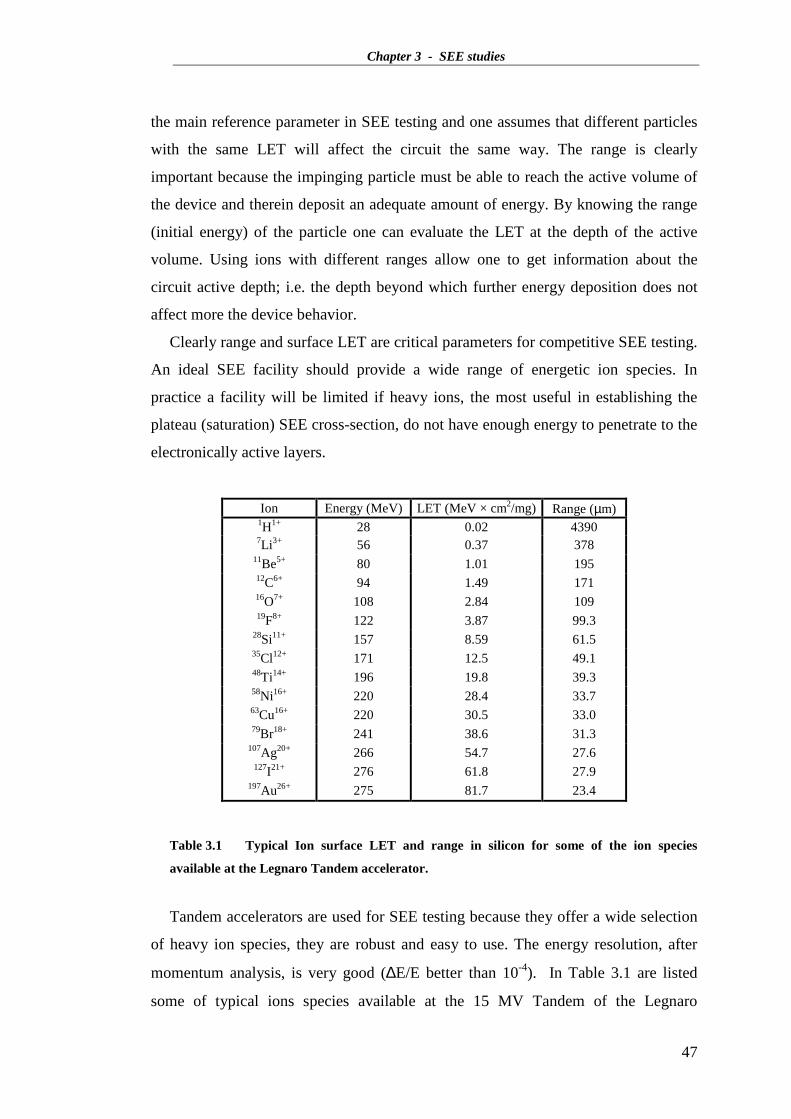
Chapter 3 - SEE studies
47
the main reference parameter in SEE testing and one assumes that different particles
with the same LET will affect the circuit the same way. The range is clearly
important because the impinging particle must be able to reach the active volume of
the device and therein deposit an adequate amount of energy. By knowing the range
(initial energy) of the particle one can evaluate the LET at the depth of the active
volume. Using ions with different ranges allow one to get information about the
circuit active depth; i.e. the depth beyond which further energy deposition does not
affect more the device behavior.
Clearly range and surface LET are critical parameters for competitive SEE testing.
An ideal SEE facility should provide a wide range of energetic ion species. In
practice a facility will be limited if heavy ions, the most useful in establishing the
plateau (saturation) SEE cross-section, do not have enough energy to penetrate to the
electronically active layers.
Ion Energy (MeV) LET (MeV × cm2/mg) Range (µm) 1H1+ 28 0.02 4390 7Li 3+ 56 0.37 378
11Be5+ 80 1.01 195 12C6+ 94 1.49 171 16O7+ 108 2.84 109 19F8+ 122 3.87 99.3
28Si11+ 157 8.59 61.5 35Cl12+ 171 12.5 49.1 48Ti14+ 196 19.8 39.3 58Ni16+ 220 28.4 33.7 63Cu16+ 220 30.5 33.0 79Br18+ 241 38.6 31.3
107Ag20+ 266 54.7 27.6 127I21+ 276 61.8 27.9
197Au26+ 275 81.7 23.4
Table 3.1 Typical Ion surface LET and range in silicon for some of the ion species
available at the Legnaro Tandem accelerator.
Tandem accelerators are used for SEE testing because they offer a wide selection
of heavy ion species, they are robust and easy to use. The energy resolution, after
momentum analysis, is very good (∆E/E better than 10-4). In Table 3.1 are listed
some of typical ions species available at the 15 MV Tandem of the Legnaro

Chapter 3 - SEE studies
48
Laboratories. The LET values reported are the surface LET value at the beam
energy; i.e. the values as the ion enters a piece of silicon before losing energy.
Tandems are however somewhat limited in energy. Indeed the active volumes of
the latest generation microelectronic devices are buried below several metallization
layers and to test them requires ions with greater ranges (Figure 3.2).
SEE tests are of course performed with more energetic types of accelerators
(cyclotrons, linacs, booster systems). These are less mono-chromatic, but as ion LET
and range depend weakly on energy this is not a problem. 15
Figure 3.2 A cross-section of a modern device showing the thick metallization layers
(courtesy B. Doyle). The active volumes (FETs) are 16µm below the surface.
3.2.3 Cross-section measurement
The occurrence of SEE in a device depends on the total amount of charge
collected by an active volume and this depends on the total ion path length in the
active part of the device. The SEE sensitivity is assumed to be completely described
by the geometry of the sensitive volume and the critical charge Qc associated with
the particular type of single event effect. The critical charge is the amount of charge
15 However the issue of high quality energy resolution beams is of capital importance if there is the
need for micro-focusing the beam down to micron size, a well-established technique to perform
microscopic SEE testing.

Chapter 3 - SEE studies
49
that must be collected in an active volume of the device to cause an event and
depends primarily on the circuit characteristics.
In SEE testing one wants to determine the device sensitivity as a function of the
amount of charge deposited. The path length and hence the charge deposited in a thin
layer depends on the angle of incidence of the particle and hence it is possible to
measure the SEE sensitivity over a range of charge deposition by simply varying the
angle of the beam. However, the results need to be normalized to the effects of the
beam at normal incidence. This idea leads to the concept of effective LET:
(3.9) ( ) ( )( )ϑcos0oLET
effLET = .
Device sensitivity measurements are then expressed as a function of effective
LET. This technique works if the particle reaches depth of the active volume; i.e.
range > depth/cos(ϑ).
The goal of a sensitivity test is to measure the SEE cross section as a function of
the effective LET. The experimental SEE cross section is given by:
(3.10) ( ) [ ] [ ]22
cos
LET cmfluence
countSEEcm
fluenceeffective
countSEEeffectiveSEE ϑ
σ×
==
where the effective fluence is the particle fluence of the beam (respect to a unit
surface normal to the beam) multiplied by the cosine of the incidence angle of the
beam on the tilted taget.
The results of a SEE measurement usually takes the form of a saturation-like
curve with an onset at some threshold LET which then goes to an asymptotic value at
higher LET values. The threshold LET determines the critical charge, the asymptotic
cross section gives the area of the sensitive volume. This information, combined with
the thickness of the sensitive volume, is sufficient to calculate the SEE rates of many
types of devices in any given radiation environment.
A typical test consists of a series of exposures with well-defined beams (energy
and fluence) over a range of LETs (or effective LETs) to allow a determination of the
cross-section curve. During each exposure, the device is placed under bias, either
active or passive. The SEE of interest are recognized and counted by the control

Chapter 3 - SEE studies
50
electronics driving the device during irradiation, while the particle fluence is
obtained from beam dosimetry.
For phenomena regarding memory elements, like SEU, the cross section can also
be given per bit by simply dividing the global SEU cross section by the number of
irradiated bits per unit area:
(3.11) ( ) ( )
=
bit
cm
devicebit
effectiveeffective SEE
SEE
2
into
LET LET
σσ .
SEUs in static RAMs best exemplify many aspects of SEU testing. Each RAM
cell is, to first order, identical, and from an SEE perspective, the device is easily seen
to be an array of sensitive volumes. Tests are usually performed by loading a pattern
in the memory array, exposing the device to a known fluence of charged particles at
a particular LET. The exposure is stopped and then the array is interrogated to count
the number of flipped bits, and the cross section is calculated. Since each sensitive
volume is identical, the per-bit cross section is simply the measured cross section
normalized to the number of bits in the memory array. A complete experiment uses
many LET values to obtain a full cross section curve of the SEE of interest.
The SEE cross section often depends on other factors, such as electrical bias or
temperature, and deviates from a strict dependence on effective LET. In reality, the
cross section is not a step function, but a Weibull curve (Figure 3.3) that increases
with a finite slope in the threshold region, followed by a knee region, and a gradual
approach to the asymptotic cross section. These deviations can be due to statistical
variations in the sensitive volume geometry or in the critical charge for a volume and
are significant for calculating event rates. Another source of deviation in the shape of
the cross section occurs when the unit cell has more than one sensitive volume, or
when several different types of cells are present, each with their own characteristic
sensitive volume. In such a case one may observe a stair-shape curve which is the
superposition of a many Weibull curves each with different threshold and plateau
LET values (Figure 3.4).

Chapter 3 - SEE studies
51
Figure 3.3 Representative heavy ion cross section curve with cross section expressed as a
function of effective LET. This curve has Weibull parameters: L0= 10MeV/mg/cm2,W=30
MeV/mg/cm2, shape parameter = 1.6.
Figure 3.4 The SEU cross-section experimental data and multiple-Weibull fit of the
pipeline of the APV25 frontend chip for the CMS detector at LHC. [35]
3.2.4 Proton SEE testing
Energetic protons generally do not deposit enough energy in a sensitive volume to
directly cause SEEs. However, approximately one in 104 to 106 protons undergo
reactions with nuclei of the Si atoms in the device and produce energetic residual
range nuclei (recoils or fragments). If produced in or near a sensitive volume, the

Chapter 3 - SEE studies
52
residual nuclei can deposit enough energy to cause an SEE. The residuals are short-
range ions that will deposit most or all their energy within the sensitive volume.
Proton testing proceeds much like heavy ion testing in that the sample is exercised
while exposed to a beam for a given fluence. Events are counted in each exposure,
and the event cross section is calculated by dividing the number of events by the
fluence for the exposure (recall that the effective fluence is used for heavy ion
testing). This procedure is repeated over a range of proton energies to fully
characterize the cross section as a function of energy. Three issues, however, make
proton testing significantly different from heavy ion testing. First, and foremost,
samples experience significant total ionizing dose damage when exposed to proton
beams (to obtain useful statistics in proton testing one must compensate the very
small probability of indirectly causing a SEE by irradiating up to relatively high
proton fluences, several orders of magnitude higher than those used with heavy ion
testing), and the event cross section can be different as damage accumulates. Care
must be taken to plan experiments so that the device characteristics are not unduly
altered during the measurements. Second, since the nuclear interaction probability
does not depend on the beam incident angle and the reaction products deposit nearly
all their energy in the sensitive volume, the cross section is assumed to only depends
on the proton energy. As a result, for proton testing, there is no equivalent concept to
the effective LET used in heavy ion testing. Finally, the physical layout of proton
exposure facilities and safety concerns for human experimenters adds considerable
complication to experiment and equipment design.
3.3 Radiation Effect Microscopy (REM)
3.3.1 Introduction
In previous paragraphs, an overview of device characterization with respect to
SEE sensitivity was given, and the concept of global cross section was introduced.
This type of tests provides fundamental data regarding the reliability of electronic
circuits in radiation environments: the knowledge of the cross section curve versus
LET allows one to predict how a device will be affected from a random exposure to
ionizing radiation. As the whole device, or a macroscopic portion of it, is exposed to

Chapter 3 - SEE studies
53
a broad beam, this method cannot indicate the specific reason for radiation
sensitivity. To do so would require knowing the location of the ion impacts. Device
simulations can be used very effectively to pin point the sensitive parts of a device;
e.g. determine which parts of a device are sensitive to SEE (e.g. which transistor in a
latch; which logic element in an IC; etc. etc.). But experimental data is ultimately
desirable, if only because data is necessary to validate any simulation.
Radiation Effects Microscopy (REM) provides a way to correlate device response
(occurrence of an SEE; anomalous Ion Beam Induced Charge Collection (IBICC)) to
the impact points of incoming particles. REM experiments are usually performed
with a microprobe system that systematically scans the device under test with a low-
intensity highly focused ion microbeam.
3.3.2 A REM example
A famous example of REM has been performed by SANDIA laboratories [36],
where predictions resulting from simulations with DA VINCI code and experimental
results were compared.
Two CMOS6r SRAM ICs were studied in this work, a 16 K SRAM test chip
known as the TA788, and a 256 K SRAM standard evaluation circuit (SEC) known
as the SA3953 (Figure 3.5).
Figure 3.5 Layout of 256 K 6-transistor SRAM unit cell (D = drain and S = source). The
red box indicates the boundaries of the unit cell, the green regions are the gate polysilicon
lines, and the blue lines show the interconnections within the unit cell.

Chapter 3 - SEE studies
54
The simulations were performed for energetic ion strikes incident every 0.5µm
throughout the unit cell to give a map of the SEU-sensitive area of the SRAM unit
cell. By repeating these simulations for several ion/energy combinations, the
evolution of the sensitive area as a function of ion LET has been generated, as shown
in Figure 3.6.
Figure 3.6 Evolution of the soft-error sensitive area (black regions) of a 256 K SRAM unit
cell as a function of increasing ion LET
As one can see from the picture, different parts of the circuit start begin to be
sensitive at higher LET values, and only a few components are the cause of the
radiation sensitivity of the cell. In a global irradiation experiment such a behavior
would give rise to a double step Weibull cross-section curve.
The simulation results are impressive. However they require enormous computing
time, even on a parallel supercomputer, and cannot represent a definitive verdict
about the radiation hardness of a circuit, as they rely on the many assumptions
necessary to implement a computable physical model.
To perform a direct validation of a such a rich simulation it is necessary to use an
experimental system that is capable of registering both the effect and the position of
impinging ions with a spatial resolution compatible with the feature size of the
device under test. To provide validation of the Da Vinci simulations at the level of
individual memory cells (Figure 3.7), REM experiments were performed at the heavy
ion microprobe facility on the EN tandem Van de Graaff at Sandia.

Chapter 3 - SEE studies
55
Figure 3.7 SEU image of several unit cells in a TA788 16 K SRAM obtained with 35 MeV
chlorine ions using a heavy ion microprobe and equivalent simulated SEU map for 35MeV
chlorine ions.
Figure 3.8 Left: calibrated IBICC image of several unit cells in a TA788 16 K bulk SRAM
obtained with 20 MeV carbon ions using a focused ion microbeam. Right: equivalent
simulated charge–collection map for 20-MeV carbon ions. The color scales for both maps
are the same and indicate total charge collection measured at the power supply.
In addition to the soft-error sensitive region for a given ion/energy combination,
the simulations gives the transient currents in the SRAM cell as a function of ion
strike location. By integrating the current over time it is possible to compute the total
charge collection as a function of ion strike location in an externally accessible
contact. Comparing the simulated charge–collection images to experimentally
measured calibrated IBICC images obtained from the heavy ion microprobe, is
helpful to further validate the accuracy of the simulations. Figure 3.8 shows a 20-
MeV carbon–ion calibrated IBICC image of several unit cells of the TA788 16 K
Chapter 3 - SEE studies
56
SRAM, along with the simulated charge collection. 20-MeV carbon ions have an
LET of 6 MeV-cm /mg, below the upset threshold.
The simulated and measured IBICC images generally agree to within about 20–
30%. The validation experiments shown here indicate that mixed-level device/circuit
simulation tools such as Da Vinci are well suited to SEU modeling of bulk CMOS
SRAMs.
3.4 Microbeam techniques
3.4.1 Introduction
A microbeam allows one to precisely probe SEE sensitive areas of a device. In
addition the amount of ion beam induced charge collected at specific locations on the
integrated circuit can be measured and the depth of charge collection of the device
can be calculated. These microprobe techniques, when coupled together, give a
detailed picture of the mechanisms responsible for SEE that is impossible to obtain
by other means. Microbeam techniques are also essential for transient charge
collection measurements to ensure that signal arises from only the region of interest.
When coupled with modem simulation tools, a complete picture of SEE emerges.
In the following paragraph we will discuss the main ways to implement
microbeam techniques.
3.4.2 Microbeam apparatus
The first approach consists in a placing a diaphragm with a pin-hole aperture
between the sample and a heavy-ion source (such as an accelerator) and collimating
the ion beam to a diameter of a few micrometers. The test sample, and in some cases
the aperture, is positioned on an x-y stage to move the microbeam to a specific region
of the device. Aperture sizes that can be used range from tens of µm down to about
2.5 µm. Micro-collimator systems based on glass tube micro-capillaries have also
been used with radioactive alpha sources, such as a polonium tipped wire.
Chapter 3 - SEE studies
57
A significant fraction of beam particles interact with the edge material of the
aperture and produce a wide spatial and energy distribution of background particles
(beam halo) that will affect the analysis. This limits the achievable spot size of
micro-collimator systems to about 2 µm (as distance of the aperture and the sample is
on the order of 0.5 cm). The beam halo increases with increasing atomic number and
energy. Secondly a micro-collimator system cannot be scanned rapidly. In addition
the beam current falls rapidly with the diameter of the aperture. This is problem if
high statistics experiments are to be performed on low sensitivity devices. All these
limit the effectiveness of the micro-collimator technique for studying feature sizes
smaller than a micron.
The second technique performs magnetic micro-focusing of the beam, and the
scanning of the regions of interest on the device is achieved either by a electrostatic or
magnetic means. A schematic of a magnetically focused system is shown in Figure
3.9. The beam optics is represented by a lens. In practice a microbeam facility will
include: pre-slits, a magnetic beam switch, microslits, antiscattering slits, a beam
scanning (rastering) system, a magnetic beam deflector, a lens diaphragm, the lens (a
system of magnetic quadrupoles, usually a triplet), an optical microscope, and finally
the sample stage. The optical microscope helps to aim the beam onto the target. In
addition one might include an ion impact detection system to certify the arrival of an
ion on the targeted position. This can be done by detecting the secondary electrons
emitted from the target surface when impacted by the ion. Finally the vibrations must
be reduced to acceptable levels. Vibrating pumps (turbo and cryopumps) are coupled
to the microscope chamber via soft bellows and vibration free pumps (ion pumps) are
used along the beamline between the microslits and the lens. In some facilities the
microprobe is isolated from vibrations from the floor by air springs.
To date, various microbeam facilities exist with different performances (e.g. beam
spot sizes, ions species and energies). For SEE studies the most important facilities
are:
• the heavy ion microbeam of GSI (Darmstadt, Germany). The linear
accelerator UNILAC delivers ions from C to Ur with energies between 1.4
MeV/nucleon to 11.4 MeV/nucleon. It has been operational since 1987 and
beam spot sizes of 0.5 µm are routinely achieved [37] [38];
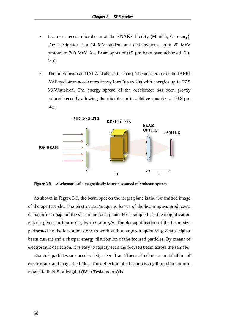
Chapter 3 - SEE studies
58
• the more recent microbeam at the SNAKE facility (Munich, Germany).
The accelerator is a 14 MV tandem and delivers ions, from 20 MeV
protons to 200 MeV Au. Beam spots of 0.5 µm have been achieved [39]
[40];
• The microbeam at TIARA (Takasaki, Japan). The accelerator is the JAERI
AVF cyclotron accelerates heavy ions (up to Ur) with energies up to 27.5
MeV/nucleon. The energy spread of the accelerator has been greatly
reduced recently allowing the microbeam to achieve spot sizes ≅ 0.8 µm
[41].
Figure 3.9 A schematic of a magnetically focused scanned microbeam system.
As shown in Figure 3.9, the beam spot on the target plane is the transmitted image
of the aperture slit. The electrostatic/magnetic lenses of the beam-optics produces a
demagnified image of the slit on the focal plane. For a simple lens, the magnification
ratio is given, to first order, by the ratio q/p. The demagnification of the beam size
performed by the lens allows one to work with a large slit aperture, giving a higher
beam current and a sharper energy distribution of the focused particles. By means of
electrostatic deflection, it is easy to rapidly scan the focused beam across the sample.
Charged particles are accelerated, steered and focused using a combination of
electrostatic and magnetic fields. The deflection of a beam passing through a uniform
magnetic field B of length l (Bl in Tesla metres) is

Chapter 3 - SEE studies
59
(3.12) ( )2
48.3sin
QEA
Bl=θ .
while the deflection of a beam passing through a uniform electrostatic field V/d
(Vm-1) of length l metres is
(3.13) Ed
VQl
⋅⋅=
−7105tanθ .
where A is the particle mass, Q is its charge and energy E is expressed in MeV.
The much higher effectiveness of magnetic bending in curving high energetic
particles makes it the most used way to bend ion beams.
The usual way to focus MeV ions is through quadrupole lenses (Figure 3.10).
Figure 3.10 Quadrupole lens schematic. Beam direction is toward the page.
A magnetic quadruple consists in four poles arranged symmetrically about the
beam axis generating a hyperbolic field profile normal to particle motion axis. In the
illustrated configuration the field is normal respect to the beam axis, so ensuring
strong force applied toward the axis, a fundamental condition to allow beam
focusing. Note that this kind of lens focuses the beam along one axis while it
defocuses the beam along the orthogonal one: this means that to focus the beam in
both axis at least two carefully matched quadrupoles are needed (doublet
configuration). To get submicron beam focusing (high demagnification ratio), at
present both triplet (“Oxford”) and quadruplet (“Russian”) multi lens system are used
(Figure 3.11).

Chapter 3 - SEE studies
60
Figure 3.11 Common microbeam lenses configurations.
At present the best performances for a microbeam (in term of resolution) belongs
to the group of F. Watt at the University of Singapore [42]: using an Oxford OM-
2000 triplet, a 3 MeV proton beam is focused down to a spot of 300 nm by 400 nm in
size. This is truly an impressive result, but it is practically of no interest in the field
of Radiation Effects Microscopy as it is difficult to maintain similar levels of
performance with high mass high energy ions. No significant improvements in
spatial resolution have been reported in over 5 years. To understand the reason of this
stagnation, we need to consider the main causes that set a limit to the practical
resolution obtainable with a microbeam.
Several factors limit the final resolution in a microbeam system, i.e. the beam spot
size on the target. Some of them are engineering issues and presumably it would be
possible to solve them. They span from mechanical stability (vibrations, long term
drift due to thermal changes, for instance) to stray magnetic fields. Also scattering
from residual gas in vacuum can contribute to worsen the resolution.
On the other hand two main issues are directly related to microbeam systems.
First, a microbeam works by projecting a demagnified image of an object, the slit
aperture. When the beam passes through the slit, particles that interact with the edge
are scattered and arrive to the optical system with different energies and direction
with respect to an ideal, parallel and monochromatic beam (Figure 3.12).

Chapter 3 - SEE studies
61
Figure 3.12 Ions scattering due to interaction with slits.
Lenses can correctly focus only particles with energy and direction inside a
narrow spread around specific values, so scattered particles are poorly focused by the
optics and form a halo around the ideally focused beam spot, decreasing the final
resolution. In table 3.2 we report the ratio of scattered ions versus direct ions for
different ranges and slit apertures.
Slit aperture (µm)
Range (µm) 20 1
60 0.060 1.2
10 0.002 0.033
Table 3.2 Ratio of scattered beam versus direct beam.
As one can see from the table, for ions with a range of 60 µm in the slit metal, the
ratio of scattered ions versus direct ions goes from 0.06 for a 20 µm aperture to 1.2
for a 1µm aperture. This means that there is a lower limit on the minimum usable
aperture size set by the increasing aberration due to scattering phenomena, and this
limit sets the smallest available beam size on target, as the demagnification is a fixed
parameter of the design.
To improve resolution, the common approach is to adopt high demagnification
systems, usually employing more sophisticated optics or multi stage systems (Figure
3.13).

Chapter 3 - SEE studies
62
Figure 3.13 Schematic of a multi-stage system.
This configuration provides for an aperture at the intermediate image plane which
removes the halo from the slit scatter. The high overall demagnification allows a
large object aperture and, as the final stage can have long working distance, it helps
design of target chamber.
It is important to note that, in principle, higher demagnifications should allow one
to use larger object slits, but in practice they are not because it usually means higher
aberrations.
The second major issue is that microbeams, like all optical systems, suffer from
aberrations due to the lenses themselves. These aberrations may be divided into two
main categories: geometrical and chromatic. Aberrations blur and deform the ideal
focused spot so degrading the overall system resolution.
Geometrical aberrations are generated by imperfections of the optical system: e.g.
the field shape is not exactly hyperbolic; the yokes are not perfectly aligned with the
beam; the power supply exhibits ripples that affect the uniformity of fields in time,
and so on. An improved engineering and/or more sophisticated optical design can
greatly reduce the effects of this kind of aberration. Instead, differently from
geometrical aberrations, chromatic aberration is an intrinsic behavior of any lens, and
cannot be corrected by improving lens manufacturing. The only way to significantly
reduce chromatic aberration is to implement a multi-lens design where the net
chromatic aberration is removed by mutual cancellations between lenses. While such
an approach is common in conventional optical system, at present ion beam optics
technology cannot provide an equivalent solution. Hence, the only practical way to
keep chromatic aberration under control is to have an extremely monochromatic
beam: the particle beam energy spread must be as small as possible and the mean
beam energy value must remains constant over time. As high-energy accelerators of
heavy ions with monochromatic beams are hard to obtain, this is by far the most
important intrinsic limitation in using a microbeam to perform Radiation Effects

Chapter 3 - SEE studies
63
Microscopy. The production of the microbeam with a spot size as small as 1µm by
quadrupole lenses requires the energy spread of the beam ∆E/E < 0.02%. Even in the
case of an ideally monochromatic beam, strong magnetic lenses are required to bend
heavy and energetic ions necessary for SEE testing.
At present, the best results in focusing down to micron size heavy energetic ions
were obtained by the microbeam at the SNAKE tandem (∆E/E < 0.01%) that uses
superconducting focusing quadrupoles. They have focused 100 MeV 16O down to a
spot diameter of 500 nm [43] and lateral resolutions as low as ∆x = 600 nm and ∆y =
150 nm have been reported.
Recent important progress has been made at the AVF cyclotron of TIARA. The
energy spread in the cyclotron beam depends on a waveform of the acceleration
voltage and beam phase acceptance of the cyclotron. The typical energy spread of the
cyclotron beam is around 0.1% in the ordinary acceleration mode using a sinusoidal
voltage waveform. Recently the energy spread was successfully reduced to allow for
submicron beam spots by superimposing a fifth-harmonic voltage waveform on the
fundamental one to generate a flat-top waveform for uniform energy gain.
3.4.3 REM limits
The main limitation of microbeam is the difficulty to work with energetic heavy
ions necessary for SEE sensitivity measurements. In addition, as new circuits grow in
complexity, the direct irradiation of the front surface of a device becomes more
difficult to do because of the presence of structures and several micron thick layers
of metallization for surface electrical contacts (Figure 3.14 a) that can affect the
beam before it reaches the sensible nodes of the circuit.
In the case of ASICs or R&D test structures, it is generally possible to obtain
tailor-made samples especially conceived for REM investigations. But for the
growing majority of standard production devices (COTS) a similar procedure is
clearly not possible.16 The dense layers and superstructure will clearly degrade the
energy of the impacting heavy ion. This is an important problem when one considers
that not all SEE depend only on the charge induced in the thin (~1 µm) active layer
16 In any case the plastic case should be removed.

Chapter 3 - SEE studies
64
of the device. For instance a SEL involves the collection of charge from depths
extending for several micrometers and it is generally considered appropriate to test
for SEL using ions for which the range in silicon is at least about twice the epitaxial
layer thickness. Nonetheless, space agencies (NASA, ESA) require dedicated
validation measurements with greater range ions to remove all doubts about SEL rate
test. These considerations exemplify the importance of developing irradiation
facilities at ion accelerators at even higher energies.
A feasible approach for SEE irradiation at higher energy ion accelerators consists
in irradiating the sample from the backside thereby avoiding all the surface structures
on the top side. This technique requires a back-thinning procedure to reduce as much
as possible the thickness of the silicon substrate (Figure 3.14 b). Anyway it requires
that the ions travel through the substrate for several tens of microns (∼50 µm, in the
example) before reaching the sensible structures on the front surface of the device.
Figure 3.14 Hyunday 256-Mbit SDRAM, front side (a) and back-thinned sample (b)
(Courtesy of ESA)
This trend, requiring high range, hence high energy heavy ions, is difficult with
microbeams for two reasons. First, as already stated, it is difficult to focus heavy
energetic ions. Second, to accelerate ions to even higher energies requires
accelerating machines different from electrostatic accelerators such as Tandems that
are the most suitable for microbeams. Microbeams are used in combination with
electrostatic accelerators because they provide the highly monochromatic and stable
beam necessary for the microbeam optics to achieve micron resolutions. In table 3.1
we list the typical ion species and energies deliverable by a big electrostatic
accelerator (15 MV Tandem of the INFN Legnaro National Laboratory). The values

Chapter 3 - SEE studies
65
listed well represent the practical upper limit to the energies obtainable by such kind
of machines. Note that for LET values higher than 20 MeV×cm2/mg (48Ti at 196
MeV) the ion range in silicon falls under 40 µm, a value that is considered a lower
limit to allow performing backside device irradiation.
To obtain higher range heavy ions for future state-of-the-art SEE testing requires
using a different type of accelerator system, such as using RFQ boosters at the exit of
an electrostatic accelerator, cyclotrons or even more complex accelerator systems.
Cyclotron accelerators and boosting systems, while able to deliver heavy ions with
higher energies, even higher than 1 GeV, do not ensure the beam monochromaticity
and stability necessary for microbeam systems.
For SEE testing there is at present the need to ensure good resolutions for very
energetic (high range) ions over a very wide range of heavy ion species (high Z for
high LET). It is important to note that the feature size of state-of-the-art electronics is
less than 100 nm, more than a factor three smaller than the very best microbeams. It
unlikely that microbeam resolutions will improve much. On the other hand electronic
technology continues to evolve and feature sizes continue to shrink.17 No foreseeable
microbeam design will ever reach comparable resolutions.
We conclude that present REM techniques are limited when evaluated in terms of
present and certainly future requirements for SEE testing with heavy ions with high
LET and large range values. This is the reason for the necessity to have an alternative
and flexible approach to Radiation Effect Microscopy, that we are going to describe
in the following chapter.
17 The feature size of present technology is already comparable to the lateral spread of the ions due
to multiple scattering in the metallization layers ∼10µm.

Chapter 3 - SEE studies
66

Chapter 4 - Ion Electron Emission Microscopy
67
4 Ion Electron Emission Microscopy
4.1 An alternative approach
4.1.1 Introduction
An alternative to the traditional microbeam technique, Ion Electron Emission
Microscopy, was first proposed in 1999 and developed by the group of B. L. Doyle
at SANDIA National Laboratory [44].
This approach discards the need for precisely focused and scanned ion beams and
uses a broad (non-focused) beam (Figure 4.1).
Figure 4.1 Schematic of IEEM technique: the position of the impinging ions is revealed by
imaging the emitted secondary electrons.
Instead of relying upon the scanning system to know where the ion beam spot is
when a radiation effect is detected, the IEEM technique precisely images the position
of the secondary electrons emitted from the surface of the target as a result of single
ion impacts. The secondary electrons are collected by a series of electrostatic lenses
Chapter 4 - Ion Electron Emission Microscopy
68
and the magnified secondary electron image of the target surface is projected onto a
focal plane. To reconstruct the impact points of the impinging ions the electron
emission points of the hit surface are imaged by coupling the electron emission
microscope to a fast two-dimensional position detector that gives the spatial
coordinates of the ion impacting with micrometric resolution. The detector time-
resolves individual ion hits in the field of view of the microscope up to impact rates
of several kHz. The timing of the emissions of secondary electrons at the mapped
positions on the sample surface is correlated with the ion-induced signals from the
device or material sample under test to match a particular ion interaction to a
particular place on the sample.
It is important to keep in mind that the IEEM technique is not perfectly equivalent
to traditional microprobes. The possibility to aim with micrometric precision at the
target is a prerogative of microbeams and this is an extremely useful feature when
one has a reason to test a very specific spot of the device under test. An IEEM
instead furnishes only the precise coordinates of random ion impacts in a small area
(hundreds of square microns). A systematic scan with a microbeam or the random
IEEM technique are used when the user does not know “a priori” which spots of the
device are more critical.
The traditional microbeam approach is arguably the preferred one, as one can
decide where the next ion is going to strike, but it needs by far greater development.
It is very challenging to focus to micron size a wide variety of energetic heavy ion
beams. A competitive SEE heavy ion microbeam facility for modern microelectronic
devices is invasive and requires great technical, human and economic resources to
develop and implement. On the other hand an IEEM is relatively simple, not too
expensive and compact; i.e. it can be easily installed and used by a relatively small
group of people at high energy heavy ion accelerators, such as cyclotrons and post-
accelerators that deliver ions with great range and are more suitable to test the latest
microelectronic devices.
4.1.2 Secondary electron emission – generalities
The physical mechanism at the basis of Ion Electron Emission Microscopy is the
emission of secondary electrons from the target surface as a consequence of an ion

Chapter 4 - Ion Electron Emission Microscopy
69
strike. The average number of secondary electrons emitted for each impact depends
on the interaction of that particular ion with the target surface and is an important
parameter for an IEEM since it sets the efficiency of this technology [44].
According to the theory of Sternglass, the physics of secondary electron
production involves three stages:
• formation of secondary electrons: the energy lost by fast ions is given up
in two types of collision processes: elastic collisions where low energy
(1÷20 eV) secondary electrons are produced; inelastic collisions that give
rise to energetic knock-on electrons (δ rays) which, in turn, produce
secondaries that may then produce tertiaries, and so on, in higher order
collisions. Although the number of δ rays is very small, the total energy
going into their formation approximately equals that going into the direct
formation of slow secondaries at high ion velocities;
• secondaries diffusion: low energy secondaries move by diffusion through
the medium. Elastic collisions involve small amount of energy transfer to
the thermal vibrational modes of the lattice and it takes on the average
only a few collisions (2÷5) to reduce the energy of a secondary below the
minimum value necessary to overcome the surface barrier potential.
Considering that the mean free path between collisions in metal is
approximately of the order of a nanometer, escaping secondary electrons
are only those produced at shallow depths in the target, about 1÷5 nm
below the surface;
• emission into vacuum by overcoming the surface barrier, which is the
surface dipole potential, originated by the asymmetry in the electron
charge cloud of the surface atoms projecting outward beyond the positive
charges of the ion core.
According to Sternglass theory [45], the electron yield Y (i.e. the average number
of secondary electrons able to escape from the surface for ion impact) is:
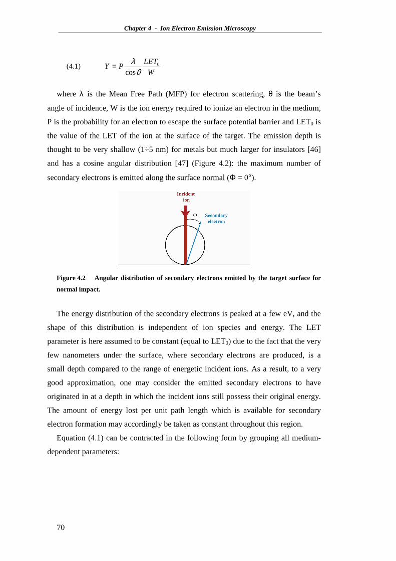
Chapter 4 - Ion Electron Emission Microscopy
70
(4.1) W
LETPY 0
cosθλ=
where λ is the Mean Free Path (MFP) for electron scattering, θ is the beam’s
angle of incidence, W is the ion energy required to ionize an electron in the medium,
P is the probability for an electron to escape the surface potential barrier and LET0 is
the value of the LET of the ion at the surface of the target. The emission depth is
thought to be very shallow (1÷5 nm) for metals but much larger for insulators [46]
and has a cosine angular distribution [47] (Figure 4.2): the maximum number of
secondary electrons is emitted along the surface normal (Φ = 0°).
Figure 4.2 Angular distribution of secondary electrons emitted by the target surface for
normal impact.
The energy distribution of the secondary electrons is peaked at a few eV, and the
shape of this distribution is independent of ion species and energy. The LET
parameter is here assumed to be constant (equal to LET0) due to the fact that the very
few nanometers under the surface, where secondary electrons are produced, is a
small depth compared to the range of energetic incident ions. As a result, to a very
good approximation, one may consider the emitted secondary electrons to have
originated in at a depth in which the incident ions still possess their original energy.
The amount of energy lost per unit path length which is available for secondary
electron formation may accordingly be taken as constant throughout this region.
Equation (4.1) can be contracted in the following form by grouping all medium-
dependent parameters:

Chapter 4 - Ion Electron Emission Microscopy
71
(4.2) θcos
0LETY Λ= .
The Λ parameter represents the medium respect to ion induced secondary electron
emission and ranges, for smooth metal surfaces. Its value is reported to range
between 0.07 and 0.13 Å /eV (in the energy range from 80 keV to 1 MeV [48]), but
can be significantly reduced by surface structures/defects that perturb the electric
field uniformity.
The most important approximation made in (4.2) was to assume the extraction
work to be independent from the ionization track generated by the ions: while this is
a good approximation for lighter ions (protons), ionization becomes relevant for
heavy ions. As a consequence of the strong ionization of heavy ions, the secondary
electron yield is significantly diminished and the Λ parameter is not a constant but it
depends on the ion species and energy [46].
As no experimental data on the electron yield from gold surfaces from energetic
heavy ions available at SIRAD was present in literature, specific measurements were
performed at SIRAD using a wide selection of ions [76]. We used three Au targets
(one bulk and two thin gold deposition, 70 µg/cm2 and 200 µg/cm2 on 2 µm thick
mylar). Measurements were also made using an aluminum (oxidized) target.
In figure 7.15 we show the experimental yield data for the Au target of table 7.4
as a function of the atomic number Z. The figure also shows the expected values at
SIRAD with the tandem at 14 MV and using the highest probability charge states.
The dashed black curve shows the expected yield if one naively assumes it to be
proportional to the LET of the ion, while the red diamonds, joined by the red dashed
curve, are the expected yields for the typical ions and energies available at SIRAD
according to fit function:
(4.3)
⋅⋅= −o
A02 eVLETZaY b
For Au targets the best fit parameters are a = 0.168 ± 0.015 Å/eV and b = 1.561 ±
0.035 using the LET0 (eV/ Å) values of SRIM2003. The best fit function represents
the average yields value, the effective secondary electron emission by ion impact on
Au following Poisson statistics, as shown by Itoh et al. [77] for ions with Z ≥ 10. For

Chapter 4 - Ion Electron Emission Microscopy
72
Al 2O3 the best fit parameter values we obtained are a = 0.268 ± 0.041 Å/eV and b =
1.51 ± 0.06.
0
50
100
150
200
250
300
0 10 20 30 40 50 60 70 80
atomic number Z of ion
seco
ndar
y el
ectr
on y
ield
Y
typical SIRAD ionsand energies
with Tandem at 14 MV
Au targetY≈≈≈≈ 0.05 x LET(eV/Å)
Figure 4.3 The mean number of secondary electrons Y emitted from a gold target
expected at SIRAD as a function of the atomic number Z of impinging ions. The data points
are the values obtained at SIRAD. The red diamonds, joined by the red dashed curve, are
the expected values according to the fitting function 7.2. The black dashed curve is the
expectation assuming naively that Y be proportional to the LET.
We note that the mean energy of emitted electrons and energy spread are
important factors for electron emission microscopy as they affect the final resolution.
In the same experiment we measured that secondary electrons are emitted form Au
surfaces with energies up to around 5 eV.
While the above picture is a good approximation for metals, matter is quite
different in the case of insulators where slow electrons cannot lose their energy by
elastic collisions with conduction electrons and this results in an increased free mean
path. The increased path length and the inelastic collisions that characterize the
transport of electrons in semiconductors/insulators make the path of the secondaries
much more complicated than that described in conductors. Moreover in
semiconductors and insulators the medium ionization is a threshold process, because
the ion energy loss per interaction is higher that the small amount we found in

Chapter 4 - Ion Electron Emission Microscopy
73
conductors. In addition charge-accumulation effects increase the surface potential
barrier. For these reasons the emission yield for semiconductors and insulators is
greatly reduced, if not absent at all. This is of great importance as many
semiconductors devices present protective passivated layers (SiO2) on their surface,
making them potentially unsuitable for the IEEM technique unless their surfaces are
first suitably treated.
Measurements performed by the Doyle group observed no emission from the
passivated surface of a PIN diode [44]. This indicates the need to perform some kind
of surface preparation in the case of a non-emitting sample. This preparation should
provide a sufficiently high secondary electron yield to allow the IEEM to detect ion
impacts with reasonable efficiency.
4.2 Electrons imaging
4.2.1 Imaging electrons
The field of electron emission microscopy is approximately 40 years old and has
been reviewed by several authors, most recently by Griffith and Engel [49]. Emission
microscopy in general is a direct imaging technique. In other words, the image is not
formed by scanning a beam or sequential composition, but by collecting all the
information from the electrons over the whole field of view and in real time, two
features that are shared by IEEM.
Electron emission from surface can be induced in various ways: thermally, via
excitation by photon irradiation or electron/ion bombardment or by field emission.
Among the wide range of possibilities offered by the electron microscopy, Photon
Electron Emission Microscopy (PEEM), which uses electrons extracted from UV
photons to image the sample surface, is suitable to be used as off-the-shelf
technology to implement Ion Electron Emission Microscopy. Therefore the imaging
core of an IEEM is a commercial PEEM microscope (Figure 4.3).
A variety of contrast generating mechanisms contribute to distinguish surface
features on a submicron scale. The small energy of the electrons used to form the
image (~ 1 eV) accounts for the surface sensitivity of the PEEM: contrasting

Chapter 4 - Ion Electron Emission Microscopy
74
techniques are used to study slight variations of electron energy due to surface
features. Contrast techniques are not applicable for IEEM: the secondary electrons
emitted by ion impact are more energetic electrons (~ 5 eV) and less sensitive to
surface imperfections. Indeed the different purpose of IEEM is to provide a
measurement of the impact position of an ion and to this end the SE average yield is
the main consideration. In an IEEM experiment the ideal situation is obtained when
the yield is high and constant across the sample for uniform ion detection.
Figure 4.4 The disassembled PEEM column; two electrostatic lenses are visible.
The electron optical column of the microscope is formed by several electrostatic
elements shown in Figure 4.4: the objective lens, the zoom lens, two projective
lenses and finally the X Y position sensitive detector (PSD).
The magnification ranges from 160× to 1600× (when projector A is not used, the
magnification increases to 8000×) which corresponds to a field of view between 250
and 25 µm. The magnification is set by adjustments to the zoom lens, focusing is
performed with the objective lens, and projector B is adjusted so that the field of
view fills the PSD.
The sample surface itself is part of the objective lens. This lens is basically an
immersion lens formed by four electrodes (a tetrode lens): the sample surface and a
three electrode lens (Figure 4.5).

Chapter 4 - Ion Electron Emission Microscopy
75
Figure 4.5 Schematic diagram of the five PEEM lenses system and the diaphragms.
An accelerating field of the order of several kilovolts per millimeter is applied
between the sample and the first element of the lens (transfer voltage). The field
strength and its uniformity are a key figure to determine the best lateral resolution.
Keeping the sample at ground or at least near ground potential simplifies handling
and current measurements; however, it also requires that the whole column is at the
transfer potential (up to 15 kV in our case) with the sample positioned at a distance
of a few (3÷5) millimeters from the first lens element, allowing a maximum field
strength of ~5 kV/mm.
Figure 4.6 Internal view of the objective immersion lens of the PEEM.
The homogeneous electric field between the sample and the first lens electrode
accelerates the electrons and forms a virtual image below the sample surface. The
three electrode lens forms a magnified real image behind the objective lens.
The zoom and two projector lenses account for the final magnification on the
image detector. An aperture in the source plane of the projector B limits the field of

Chapter 4 - Ion Electron Emission Microscopy
76
view. This aperture is useful to limit the area of the sample where SEs are produced
and also to protect other areas from ion induced damage (particularly important for
testing semiconductor electronic circuits) but is not needed in many cases. The zoom
lens is used to set the total magnification. Two imaging modes are accessible; a low
magnification mode and a high magnification mode. High magnification mode
means a high field strength in the zoom lens. In this mode, the objective lens forms a
real magnified image in front of the zoom lens, which is further magnified onto the
aperture of the projector lens B. Low magnification mode means a low field strength
in the zoom lens. In this case, there is not a real but only a virtual intermediate image
formed. Switching between the imaging modes accounts for a flip in the observed
image.
A further lens (decelerating lens) with a separate power supply placed after the
last projective lens can decelerate electrons down to ~1 keV to optimize the
performances of the electron amplifier (usually a Micro-Channel Plate, MCP) placed
on the microscope focal plane. This lens can be excluded if required.
4.2.2 Resolution
Like any other “optical” instruments, the PEEM microscope presents problems of
distortion and aberration. Distortion causes an information modification (geometrical
distortion), but not its complete and definitive loss or degradation: as information is
only changed, a subsequent image analysis can restore it to its original appearance.
On the contrary, aberrations lower the resolving power of the instrument and lead to
an unrecoverable loss of spatial information.
An extracted secondary electron will enter the PEEM column with a starting angle
to be transported to the focal plane. The spread in energy and emission angle of the
secondary electrons will introduce aberrations; i.e. electrons following non-ideal
trajectories will not be focused and the image will blur. Spherical aberrations will not
occur along the optical axis of the system, while they increase when the starting
angle of the electrons diverges respect to the optical axis. By using a high electric
field strength at the surface most electrons will be transferred into the PEEM column,
even those electrons emitted up to nearly 90°. On the other hand the energy spread of
the secondary electrons leads to energy-dependent trajectories (chromatic

Chapter 4 - Ion Electron Emission Microscopy
77
aberration). The easiest way to limit both spherical and chromatic aberrations is to
put a diaphragm with an aperture that cuts electrons with improper trajectories. A
small aperture will select small starting angles and small energies, but the
transmission efficiency (the fraction of secondary electrons accepted by the PEEM)
is reduced. A good lateral resolution can only be achieved with a small contrast
aperture and a high extraction voltage.
The PEEM was designed and tested to work with electrons generated by UV
photons, that exhibit a low energy mean value (1 eV) and a narrow energy
distribution (1 eV FWHM); using a PEEM to image more energetic and less
monochromatic electrons generated by ion impacts will affect the resolving power.
In order to get a quantitative estimation of the PEEM resolution when used as an
IEEM, the Sandia team, in collaboration with the PEEM manufacturer, performed a
ray-tracing calculation of the theoretical resolution (for chromatic aberrations only)
and transmission efficiency versus aperture size [44].
Figure 4.7 Efficiency and resolution as a function of the diameter of the aperture of the
contrast diaphragm of the PEEM for both photon induced secondary electrons and high
energy ion induced secondary electrons, assuming electron mean energies of 1eV and 5eV
respectively.
For these calculations the energy distribution of secondary electrons at the sample
was assumed to be peaked at 5 eV with a 5 eV FWHM and to be emitted with a

Chapter 4 - Ion Electron Emission Microscopy
78
cosine angular distribution. With these assumptions the intrinsic resolution of the
IEEM is ∼ 500 linear resolved points (lrp); i.e. it is possible to distinguish 500
equally spaced points lined up along the diameter of the field of view (FOV). Using
the largest 300µm aperture, to maximize electron transmission and hence ion
detection, the IEEM resolution is ∼0.6 µm and the transmission efficiency is ∼ 30%
(Figure 4.6). With the 300 µm aperture the PEEM is 100% efficient with a resolution
of ∼ 0.2 µm (the intrinsic resolution of the PEEM is ∼1500 lrp). For the IEEM to
achieve a 0.2 µm resolution would require a ∼100 µm aperture but the transmission
efficiency would be only ∼ 2÷3%.
4.2.3 Electron detector
For each ion impact, a number of electrons are emitted but only a fraction of them
is transmitted by the microscope column. An electron multiplier is placed on the
focal plane of the microscope to make a robust electronic signal. This detector must
not degrade the intrinsic spatial resolution of PEEM and must have a refresh rate fast
enough to sustain a useful rate of ion impacts in the microscope field of view.
The commonly chosen detector for this kind of application is a multi stack
Microchannel plate (MCP). A microchannel plate is an array of miniature electron
multipliers oriented parallel to one another. Typical channel diameters are in the
range of 5-100 µm and have length to diameter ratios (α) between 40 and 100.
Channels are typically normal to, or biased at a small angle (∼ 8°) to the MCP input
surface. The channel matrix is usually fabricated from a lead glass, treated in such a
way as to optimize the secondary emission characteristics of each channel and to
render the channel walls semiconducting so as to allow charge replenishment from
an external voltage source (Figure 4.7). Each microchannel is a continuous-dynode
electron multiplier, in which the multiplication takes place under the presence of a
strong electric field. A particle or photon that enters one of the channels through a
small orifice is guaranteed to hit the wall of the channel due to the angle of impact.
The impact starts a cascade of electrons that propagates through the channel, which
amplifies the original signal by several orders of magnitude (104-107) depending on
the electric field strength and the geometry of the micro-channel plate. After the
cascade, the microchannel takes time to recover (or recharge) before it can detect

Chapter 4 - Ion Electron Emission Microscopy
79
another signal. MCPs show excellent time resolution (< 100ps) and a spatial
resolution limited only by the channel dimensions and spacing. Detection efficiency
of a microchannel plate depends upon the type, energy and angle of incidence of the
primary radiation and the first strike conversion of the microchannel plate. Under
common operating conditions, the detection efficiency is limited by the open area
ratio (channel area/ total plat area), since events striking the inter-channel area are
not typically collected. The open area ratio for standard MCPs ranges between 55-
85%.
Figure 4.8 A channel electron multiplier.
The typical working voltage is ∼1kV, corresponding to a gain of about 104.
Higher gains (up to 109) can be achieved by coupling two or more into stacks. In
imaging applications it is usual to express the spatial (lateral) resolution of an
instrument in line pairs per millimeters (lp/mm). For a single high resolution MCP
the limiting resolution is 40 lp/mm; for a two stack (chevron) it is better than 25
lp/mm; for a three stack (Z-Stack) high gain assembly it drops to 16 lp/mm. Still
higher gain solutions (5 plates stack) further drop the resolution performance. MCP
sizes (the diameter of the circular active area) are standard, and the most common are
18 mm, 25 mm and 40 mm and the choice of the proper sensor size depends on the
resolution requested by the specific application.
In paragraph 4.2.2 we expressed the resolving power of the IEEM in terms of lrp
(the maximum number of distinguishable points lined up along the diameter of the
field of view). When resolution is stated in lp/mm, the width of the line, i.e. the size
of smallest resolvable feature, is equal to 2 × resolution expressed in lp/mm. As an
example we consider a large diameter three stack MCP assembly. The resolution of a

Chapter 4 - Ion Electron Emission Microscopy
80
such a detector is better than 16 line pairs (lp)/mm. For a detector with a diameter of
40 mm, this corresponds to a resolution better than (2 × 16 lp/mm) × 40 mm = 1280
lrp across the diameter. Such a detector will not degrade the IEEM intrinsic resolving
power (∼500 lrp). It must be noticed that this is also true for a smaller MCP diameter
of 25 mm which will have a resolution better than 800 lrp18.
For IEEM applications, an MCP is used in high gain (saturation) mode, i.e. the
output signal strength is only weakly dependent on the number of incoming
electrons. This feature is useful to discriminate real events against dark counts from
thermally generated electrons (typically of the order of ∼ 0.5 cts/s·cm2 and increasing
with the gain factor). In fact, electrons thermally generated inside the chevron MCP
have an output signal significantly weaker than real events. Of course, for electrons
thermally generated near the input of the first stack, the discrimination will be nearly
impossible, as their output signal will be comparable with the one from a real ion
impact.
Saturation is also a desirable condition because it ensures a stable output, which
does not depend too much on the statistic of secondary electron emission, their
transport through PEEM column and the MCP amplification factor. This stable
output makes easier the coupling with a Position Sensitive Detector (PSD) device.
The time resolution of an MCP is related to the avalanche evolution time, and is
of the
order of few ns for a multi-plate stack. The avalanche electronic signal, thanks to
its prompt response to events, should be hence the ideal candidate to provide (unless
noise-pickup problems) a fast trigger signals.
18 However in UV-mode the intrinsic resolution of the PEEM is three times better than when used
as an IEEM (see Figure 4.6) and the 25 mm diameter MCP assembly would be inadequate for PEEM
applications.

Chapter 4 - Ion Electron Emission Microscopy
81
4.3 Ion Electron Emission Microscope at SIRAD
4.3.1 General description
The Ion Electron Emission Microscope installed at SIRAD irradiation facility (see
section. 4.5) uses to image electrons the same commercial PEEM from Staib [50] of
the SANDIA team. The contrast diaphragm has 200 µm of diameter, which set the
transmission efficiency to 70% and the achievable resolution in PEEM operations to
0.4 nm.
The ion beam passes down through the MCP and along the microscope lenses
(axial configuration) and strikes the sample orthogonally (Figure 4.8). The position
detector of the SIRAD IEEM doesn’t directly detect the electron avalanches at the
output of the MCP output, but it detects flashes of light from a phosphor screen
coupled directly to the output of the MCP. The avalanche electrons from the MCP,
initiated by the secondary electrons from a single ion impact, excite a phosphor
screen that emits a burst of photons [51]. These are reflected by a 45° mirror and
extracted from the vacuum chamber through a quartz window and focused onto an
external image intensifier. The regenerated light signal is finally focused onto a
custom-made, digital, high rate and high resolution position sensitive detector which
detects the photons and returns the x and y coordinate of the original ion impact. This
sensing solution has been nicknamed STRIDE, which stands for Space & Time
Resolving Imaging DEvice. The device is connected to the control PC via an USB
connection and has no need of any further external hardware.
A remote controlled sample holder, with three degrees of freedom (three linear
motorized stages (2.5 mm travel range) allows target positioning with a resolution of
0.01 µm with a repositioning error better than 0.1 µm [52] and is suited for high
vacuum (down to 1×10⁻⁷ mbar).
The same computer controls the proprietary data acquisition system, the DC
motor stage, the dosimetry software and the vacuum logger, without the need of
other external electronic module.

Chapter 4 - Ion Electron Emission Microscopy
82
Figure 4.9 Schematic drawing of SIRAD IEEM setup.
4.3.2 The irradiation chamber
The irradiation chamber has a box-liked shape and a whole side opens like a large
drawer allowing easy access to the target, to the 3 axis sample holder and to ancillary
electronics (if any). The entire sample holder and every item inside the chamber are
mounted on the sliding floor of the drawer. Thus, by opening the chamber everything
inside slides out completely from the chamber providing tabletop-like working
conditions (Figure 4.9).
The relatively small volume of the chamber (70 × 40 × 50 cm of dimensions)
allows reaching the operational vacuum level (∼ 1 × 10⁻⁶ mbar) in a reasonable
amount of time. The chamber provides enough space to host ancillary electronics that
might have to be kept ad close as possible to the target DUT.

Chapter 4 - Ion Electron Emission Microscopy
83
Figure 4.10 View of a target mounted on the sample holder with linear DC motor stages
inside the extracted drawer of SIRAD IEEM irradiati on chamber.
Two DN160CF flanges with D-style multi-pin connectors (one with 8 × 15 sub-D
type feedthrough and one 2 × 50 sub-D type feedthrough) allows a wide possibility
of connections between the vacuum chamber and any external setup (DC motor
controllers, beam diagnostic, sample DAQ, etc.) In case of need, it is possible to add
flanges with special connections without changing anything in the setup by means of
the user serviceable flanges (Figure 4.10).
Two flanges are oriented 75° respect to the PEEM axis and aim at the target plane.
One of these hosts a quartz viewport for a UV lamp. Before the experiment,
preliminary calibrations and tests are in fact performed using UV photons, to help
alignment and fine focusing of the PEEM.
Two orthogonal pairs of Helmholtz coils outside the IEEM vacuum chamber,
centered at the position of the DUT, are used to compensate stray magnetic fields
that affect the collection of the secondary electrons and hence the formation of the
IEEM image.
At present, the chamber is rigidly mounted on a fixed stand but isolated from the
rest of the beam line. The turbo pump is mechanically decoupled by means of a
vibration dumper.

Chapter 4 - Ion Electron Emission Microscopy
84
Figure 4.11 View of axial SIRAD IEEM chamber and setup in the experimental hall.
4.3.3 Fixed membrane configuration
As already stated, the surface of a typical electronic device is usually passivated
and is an unreliable secondary electron emitter. In addition, devices to be irradiated
might have complex surface features, which could introduce unacceptable
perturbations on the electric field of the IEEM used to collect the secondary
electrons. To both ensure copious secondary electron emission and strive for perfect
electron collection, we use a Silicon Nitride (Si3N4) ultra-thin membrane with a thin
deposition of gold [53]. At first, the membrane window we used [54] [55] was 5 mm
wide, 100 nm thick with a 40 nm gold layer deposition (Figure 4.11). Ions lose a
negligible amount of energy in traversing it, so avoiding any significant energy
degradation. The window presented a flat side, where the membrane is flush with the
support frame (525 µm thick, 10 mm wide), and a deep concave side. These
membranes are very delicate and cannot be placed directly in contact with the DUT.
As a consequence, the lateral resolution of the IEEM is degraded. For this reason,
given its shape, we chose to deposit gold on the non-flat side of the membrane to
minimize the lever-arm to the DUT.

Chapter 4 - Ion Electron Emission Microscopy
85
Figure 4.12 Silson golden Si3N4 membrane 100 nm thick in a 10××××10 mm frame.
The use of this configuration was problematic for several important reasons. First,
these membranes were very wide and they bulged significantly in the electric field of
the IEEM. As a consequence, the trajectories of the electrons were perturbed and the
final image distorted. In addition, the concave shape of the support-frame of the
membrane facing the IEEM distorted the electrical field that collects the secondary
electrons IEEM (Figure 4.12 a).
Figure 4.13 Membrane with the concave side towards the IEEM head; (b) membrane with
the flat side towards the IEEM head.
The collection of the secondary electrons would be perfect for a flat membrane.
To reduce membrane distortions in the electric field of the IEEM we now use a new
500×500 µm2 ultra-thin (100 nm) membrane window of Si3N4 with a 30 nm
deposition of gold on a 200 µm thick Si window frame, mounted on a holder
independent of the DUT position. To ensure the uniformity of the electric field of the
microscope, used to collect the secondary electrons, the thick window frame is now
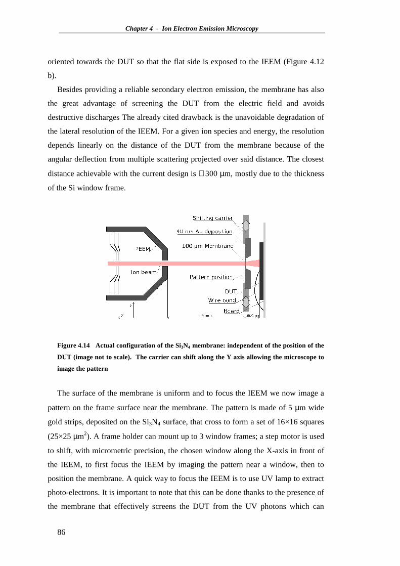
Chapter 4 - Ion Electron Emission Microscopy
86
oriented towards the DUT so that the flat side is exposed to the IEEM (Figure 4.12
b).
Besides providing a reliable secondary electron emission, the membrane has also
the great advantage of screening the DUT from the electric field and avoids
destructive discharges The already cited drawback is the unavoidable degradation of
the lateral resolution of the IEEM. For a given ion species and energy, the resolution
depends linearly on the distance of the DUT from the membrane because of the
angular deflection from multiple scattering projected over said distance. The closest
distance achievable with the current design is ∼ 300 µm, mostly due to the thickness
of the Si window frame.
Figure 4.14 Actual configuration of the Si3N4 membrane: independent of the position of the
DUT (image not to scale). The carrier can shift along the Y axis allowing the microscope to
image the pattern
The surface of the membrane is uniform and to focus the IEEM we now image a
pattern on the frame surface near the membrane. The pattern is made of 5 µm wide
gold strips, deposited on the Si3N4 surface, that cross to form a set of 16×16 squares
(25×25 µm2). A frame holder can mount up to 3 window frames; a step motor is used
to shift, with micrometric precision, the chosen window along the X-axis in front of
the IEEM, to first focus the IEEM by imaging the pattern near a window, then to
position the membrane. A quick way to focus the IEEM is to use UV lamp to extract
photo-electrons. It is important to note that this can be done thanks to the presence of
the membrane that effectively screens the DUT from the UV photons which can

Chapter 4 - Ion Electron Emission Microscopy
87
otherwise charge-up and destroy it. In addition, by mounting the membrane in a fixed
position in front of the IEEM the magnification and focus can be set once and for all,
independently of the DUT, reducing the time needed for the irradiation arrangement
(Figure 4.13).
4.4 Photons production and detection
4.4.1 Introduction
We obtain the positions of the ion impacts by imaging light spots on the phosphor
screen directly coupled to the MCP.
The output electrons of the MCP are accelerated across a small gap (∼ 1mm) and
locally excite a phosphor screen; each output electron avalanches is converted to a
blue light spot. An optical assembly, consisting of a 45° mirror (with a central hole)
and a system of lenses, collects the photons from the luminous spots and extracts
them outside the irradiation chamber where they are detected by a photon position-
sensitive detector. This is a simple and relatively inexpensive solution, but the main
drawback is that only a small fraction of the photons are collected (low optical
efficiency). To regenerate the light signal, for ease of detection, we use an external
image intensifier, which amplifies the light signal by a factor 106. The light signal
strength is now suitable to be revealed by the final position detector.
For position sensing applications the choice of sensors is very wide, but only few
solutions have been investigated. The natural approach seems to be CCD or CMOS
arrays as they offer up to mega-pixel level resolutions (our minimal requirement of
500 points on the image diameter is not an issue at all!) and the ability to work with
very low light levels. The main drawback of these arrays is the need to readout the
entire array to determine if and where the light-spot arrived and hence the difficulty
of sustaining data throughputs useful for SEE applications. A completely new digital
position sensitive detector system was hence developed [56] [57], that provides the
required high-rate and high-resolution performances. The system reduces the number
of pixels to read and makes the digital approach feasible. It will be described in the
following paragraph.

Chapter 4 - Ion Electron Emission Microscopy
88
4.4.2 Photons production, amplification and detection
A double stack MCP (40 mm large) with a central hole (8 mm diameter) has been
chosen as the main electron detector. Working in saturation mode, this device
ensures an amplification factor up to 1×10⁷ e-/e-, with a dark count rate of ∼ 0.5
counts /s·cm2, corresponding to less than 7 counts/sec on the entire area.
The 40 mm diameter phosphor screen, coupled to the MCP, converts the out-
coming electron clouds into luminous spots. Among the available types of
phosphors, the P47 (Y2SiO5:Ce,Tb) has been chosen, because its peak emission is at
400 nm, it has a fast decay time (from 90% to 10%) shorter than 100 ns with a tail
decay time (from 10% to 1%) of 2.9 µs. The light signal is short enough to allow in
the field of view of the IEEM ion impact rates well above those necessary for SEE
applications.
The MCP focal plane detector we use ensures a resolution better than 25 lp/mm,
equivalent to more than 2000 lrp over the 40 mm diameter. This is not degraded by
the phosphor layer which, thanks to its micro-crystal structure, can give resolutions
better than 100 lp/mm. A variable potential gap (0÷2 kV) between the second plate
of the MCP and the phosphor screen accelerates the electrons to increase the
phosphor conversion efficiency. The corresponding conversion yield for 2keV
electrons is ~50 γ/e-. This value refers to a single electron impinging on the screen, but
when a cloud of particles (up to 107 in a double stack MCP) reaches the phosphor, saturation
phenomena may occur. Dedicated measurements were performed to get an indicative
value of this parameter (γsat), as no specific data are present in literature [57]. Taking
into account the area of the phosphor interested by the electron current (∼ 200 µm
diameter) and the duration of the current itself (2÷4 ns FWHM), the order of
magnitude of the maximum outgoing number of photons for a single incoming
electron can be expressed as:
(4.4) ( ) γµπµ
γγγ 7222 103100
100 ≈⋅⋅=⋅⋅= nsmnsm
timeareasatyield
The light signal must be carried out of the vacuum chamber and focused onto the
PSD system. A low-distortion system of lenses has been design to perform this task.
Taking into account the transmission efficiency of this system (1%), the reflectance

Chapter 4 - Ion Electron Emission Microscopy
89
efficiency (95%) and the hole geometrical factor (6 mm diameter) of the 45° mirror
to bend the photons, the final global optical transmission efficiency is reduced to ≅
1%, corresponding to 105γ. Given this very low value, the corresponding expected
signal for 400 nm photons in a solid state detector is < 10fC, which is one order of
magnitude smaller than ENC of a typical pixel detector. We solved this problem by
adding an image intensifier, a device that amplifies the light signal to be detected by
the final sensor.
An image intensifier is a plug-and-play device that is composed by a
photocathode, an internal MCP and a phosphor screen, all items being enclosed in an
air-tight case. The image intensifier we use has a 2-stack MCP and a P47 phosphor
screen [58]. However it has a 25 mm diameter and therefore the resolving power is
25 lp/mm × 25 mm = 625 lp = 1250 lrp. It meets the time and spatial resolution
requirements for the whole system. Considering the number of photons arriving on
the photocathode (105γ), the photocathode efficiency at 400nm (30%), the maximum
gain (106 e-/e-), the acceptance factor (55%) , the phosphor yield (50 γ/e- for the P47)
and saturation effects, the expected number of out-coming photons is:
(4.5) γγ 1010≈II .
This is to be considered the maximum photon yield that it is possible to obtain
from a single electron impinging on the MCP placed at the focal plane of the PEEM.
To couple the image intensifier output with the final position sensor, additional
optics is needed. The efficiency of this optics is of the order of few percent.
Considering the maximum photon yield (4.4), the lenses efficiency (∼ 2%) and the
detector sensitivity (15%), the light level on the silicon sensor can be estimated to be
(4.6) pCpJ 1515.002.01097.410 710 ≈⋅⋅×⋅ −γ .
The last step to get a working system is to provide a fast, efficient, high-resolution
and low-noise position sensitive detector. As anticipated in paragraph 4.4.1, a
tailored 2-D detector (STRIDE), has been developed to match IEEM requirements.
In the present paragraph, I will give a brief review of the STRIDE; for a deeper and
detailed description, I refer the reader to PhD thesis work of P. Giubilato [57].

Chapter 4 - Ion Electron Emission Microscopy
90
The approach we adopted projects the light spot onto two orthogonal linear arrays
(as sketched in Figure 4.13). The number of pixels to be readout is N (the two linear
arrays are read out in parallel) rather than to N2 for a square array, while the spatial
resolution remains unaffected. A position of the peak in one linear array will indicate
the coordinate, along the direction of the linear array, of the light spot.
Figure 4.15 Schematic drawing of the IEEM bilinear sensor.
The two projections of the light signal are obtained by an optical system
consisting in a beamsplitter, that splits the original light spot into two copies, and
cylindrical lenses, placed along the two orthogonal optical paths, that squeeze each
light spot into a blade shape (Figure 4.13 and Figure 4.14). The two orthogonal light
blades are then detected by an NMOS linear array [59], chosen for its ease of use and
pixel shape (2.5mm × 50µm). The pixels are very wide and this maximizes the
collection of the photons in the light blade, important when working in these low-
light level conditions. The main drawback of the chosen sensor is its very low speed
readout rate (2 MHz). In the present prototype, the device is overclocked to 3.125
MHz, resulting in a frame rate of 3.125×10⁶/256 ∼ 12.2kframe/s.
Proprietary electronics has been developed to both drive and read the two linear
sensors. Two fast (40MHz) 12 bits ADCs (one per axis) convert the analog signal
read from the sensor into digital format. Digitized data incoming from the ADCs are
processed in parallel by an FPGA-based system, loaded with proprietary firmware.
The position of the light spot is detected and fitted. When an event has been
identified, a packet of 8 bytes is sent to the control PC via a USB connection. The
event reconstruction (i.e. the peaks matching) is implemented at software level. The

Chapter 4 - Ion Electron Emission Microscopy
91
analysis package also allows one to deal with multiple events per frame by watching
the height of the registered peaks and matching peaks of equal eight.
Bench measurements for estimating the spatial performance shows that,
everywhere in the useful area of the sensor, the resolution is better than 650 lrp
(better than 1000 lrp over 70% of the useful area), with a distortion (a systematic
error that can be corrected) under 1%.
Figure 4.16 The bilinear detector system. The optical signal is reflected upwards by a
mirror and out a viewport into a first beam splitter (a). Part of the signal is detected by a
PMT (b), the rest is reflected horizontally, regenerated by an image intensifier(c) and sent to
a 2nd beam splitter (d). Each copy of the image is squeezed (e) and detected by a linear
NMOS array (f).
4.5 PEEM imaging capability
4.5.1 The calibration target
With the experimental setup previously described, we tried to quantify the
performances of our microscope when working in PEEM mode. In the present
section I will report on a resolution measurement performed on our IEEM when
exposed to UV photon irradiation.
To measure the performances of our present setup in terms of spatial resolution,
we imaged a tailored target (Figure 4.15) used for Photon Electron Emission
Microscope calibration [60]. This target consists of a Silicon substrate (10 mm × 10
mm), with a gold pattern deposited. The pattern consists of metalized strips 10µm

Chapter 4 - Ion Electron Emission Microscopy
92
wide, separated by unmetalized regions, with widths increasing across the pattern in
steps of 0.2 µm from a minimum of 0.2 µm to a maximum of 5 µm. The
metallization layer is 35 nm Au film over 5nm Ti adhesion promoting film.
Figure 4.17 High Resolution pattern from Applied Nanotools.
We illuminated directly the target with UV photons, for which the expected
resolution is 200 nm [44]. The image reconstructed by the IEEM is shown in Figure
4.17.
Figure 4.18 UV-induced image of the calibration pattern, reconstructed by the IEEM
system.
To get from this qualitative picture a quantitative estimate of the PEEM spatial
resolution, we used the Edge Spread Function (ESF), which describes how a system
responds to a sharp straight discontinuity (i. e. to an edge). The analysis was
performed using data inside different rectangular regions like the black rectangular
region shown in Figure 4.18-a. To this end, we built histograms with the Y-

Chapter 4 - Ion Electron Emission Microscopy
93
coordinates of the data inside said regions and studied the shape of the edge; the way
the data falls from a high values in bright, emitting regions (Au strips), to low values
from non-emitting Si-regions. The edge projection was fitted with the Error Function
(erf), a special function of sigmoid shape, defined as:
(4.7) ∫
−−
⋅+=
−+x
p
yp
dyeppp
xperfpp
0
2
203
120
3
12
π
The erf, which is twice the integral of a Gaussian distribution of mean p1 and
variance σ = p3/√2, models the shape of the measured edge: the deviation from an
ideal (infinitely sharp) edge is characterized by the σ and the position of the edge is
p1.
An edge in the chosen rectangular region was fitted with an erfc and the p3
parameter was determined (see Figure 4.18). The σ value may be taken as the
estimate of the present PEEM resolution (RESPEEM). The resulting RESPEEM =
1.3±0.2 µm which is significantly worse than the theoretical value [44]. The error we
quote for RESPEEM was evaluated by considering data from different rectangular
areas.
Figure 4.19 (a) PEEM Image of the widest strips of reference target. (b) Histogram of the
the Y-coordinates of the PEEM events inside the black rectangle shown in (a) with an erf fit
(see text).

Chapter 4 - Ion Electron Emission Microscopy
94

Chapter 5 - A resolution measurement of the IEEM using at SDRAM
95
5 A resolution measurement of
the IEEM using a SDRAM
5.1 Introduction
As for every imaging device, a figure of merit of the IEEM system is the
resolution: here the ability to reveal the smallest details in the sensitivity map of an
integrated circuit. To measure the resolution we need a reference target, to be able to
precisely locate the impact position of every single ion independently by that
measured by the IEEM. In addition we need a high statistics measurement. In
practice we are looking for a device with a resolution not worse than that of the
IEEM, with a sensitive area that fills the field of view of the IEEM, that is able to
withstand an intense fluence of heavy ions (several ions/µm2) and that can be readout
with a speed comparable with the one of the IEEM (~1000 ions/s).
We identified as suitable for this purpose a memory chip, a Synchronous Dynamic
Random Access Memory (SDRAM) of the kind routinely used in computers: a 256
Mb Micron Technology high speed CMOS SDRAM, (chip model MT48LC32M8A2
-7E B).
Other commercially available pixel devices were briefly considered. Charge
Coupled Device arrays are not suitable, as individual pixels would be irreparably
damaged (stuck) by single heavy ion impacts. Flash memories are more robust, but
the information needed to reconstruct the location of the ion impact in the array is
reserved (typically not available), and it was not possible to reconstruct this
information experimentally with a method similar to that applied to the SDRAM.
When an ion impacts the SDRAM, it generates electron–hole pairs which diffuse
in the silicon substrate. The cells near the ion trajectory can collect enough charge to
undergo a bit upset, changing the value of their stored data. However the SDRAM

Chapter 5 - A resolution measurement of the IEEM using at SDRAM
96
directly provides the logical address of each cell, not its coordinates. A remapping
operation is required to associate to a logical address the corresponding coordinates.
The location of the centroid cluster of flipped-bit cells is then determined and it is
assumed to be the position of the ion impact.
To understand how we use the SDRAM it is necessary to describe how it works.
We will describe the mapping and then the experimental characterization of the
IEEM in terms of resolution and image distortions, using a high statistics data set
obtained in a heavy ion experiment.
5.2 The SDRAM system
The SDRAM chip is glued to an electronic board, electrically connected to it by
means of wire bonds that provide the power supply and the driving signals. The
SDRAM board is then connected to a Virtex-5 LX evaluation board (Avnet). The
Virtex-5 FPGA hosts the firmware that drives the SDRAM and the communication
with the control PC.
In order that the SDRAM based test system match the mechanical constraints
imposed by the IEEM environment, a custom Test Board (TB) has been
implemented. To obtain maximum readout speed using the advanced input-output
features of the SDRAM (burst mode, self refresh, etc.), the TB is based on Virtex 5, a
high performance Field Programmable Gate Array (FPGA) (see fig. 8.2). The
communication between the TB and the Test Control PC is obtained by a USB
connection.
The time information is provided to the SDRAM system by STRIDE through a
flat cable connection. The synchronization of the two systems is done the following
way: the SDRAM system is first initialized and put into an acquisition state (ready);
the STRIDE system, when started, sends a digital signal every 106 µs, the time
needed to complete the readout of the NMOS array sensors. Actually the time
resolution of the STRIDE system is given by the 2.5 MHz clock that controls the
read-out: the pixel is readout at every rising edge of the control clock and
immediately refreshed. The readout of the NMOS sensor requires 265 control clock
signals (one for each of the 256 pixels, plus 9 clock signals to reinitialize the
sequence), that corresponds to 106 µs. This time interval is the time resolution of the

Chapter 5 - A resolution measurement of the IEEM using at SDRAM
97
SDRAM system. This signal feeds a FrameNumber counter that counts the number
of frames that have been read from the beginning of the STRIDE acquisition.
The system core mapped in the FPGA is able to:
• address each cell;
• perform read and write operations;
• refresh the cells (normally every 64 ms) .
Figure 5.1 Avnet demo board, hosting a Virtex 5 FPGA. The LCD display and the rubber
keys where removed to avoid out-gasing in the vacuum chamber.
Beside these basic operations, the FPGA-based system performs complex test
procedures as:
• writes an internally generated pattern on blocks of adjacent cells (the
boundaries of this block is user defined through the control PC);
• reads the previously written block of cells;
• detects the presence of upsets;
• saves the logical address of the upset cell and its readout time and sends
this information to the control PC.

Chapter 5 - A resolution measurement of the IEEM using at SDRAM
98
In an ion beam experiment, the preliminary step is to identify the small region of
the SDRAM that is actually exposed to the ion beam (200 µm diameter area defined
by the contrast diaphragm of the IEEM). This is done using the ion beam and by
reading out the whole SDRAM: the high density of upsets immediately reveals the
position of the exposed area. We then restrict the search of upsets to the cells in the
row and column intervals that circumscribe the irradiated area and, at this point, the
actual experiment may begin. The SDRAM system continuously reads the contents
of the SDRAM cells in the selected address interval, looking for unexpected logic
values.
5.3 SDRAM output file
Every time the system detects an upset, the row and column logical addresses of
the upset, the value of the flipped bit, and the FrameNumber in which the upset
occurred are save and sent to the control-PC via the USB connection. The computer
generates an ASCII-format file in which every line is the record of the upset
information mentioned above. An example of a portion of this ASCII-file is shown
hereafter:
Bank Row Col Data FrameNumber
3 719 109 0 15344
3 890 98 8 15367
3 -890 98 8 15367
3 -890 99 8 15367
3 -890 99 8 15367
3 -890 99 8 15367
...
The size of such files can be some millions of entries.
Every entry is made up of five values:
• Bank: indicates the bank number of the upset cell. The 2nd and 4th banks
are never used because they covered by the wire bonds. The only banks
we read are 1 and 3;
• Row: the raw address of the upset cell;

Chapter 5 - A resolution measurement of the IEEM using at SDRAM
99
• Column: the column address of the upset cell;
• Data: the logic value associated to the read address;
• FrameNumber: is the number of the frame in which the upset was detected
(not to be confused with the timestamp of STRIDE which is the number
of clocks from the beginning of the acquisition).
The analysis code was written in C/C++, using the CERN Root framework [62],
and a custom function library developed by P. Giubilato and D. Contarato.
To increase the speed of execution of the analysis code, ROOT ntuples are used:
structures of entries made up of numerical values, fast to access and smaller than the
original text files of data.
Since the SDRAM is read several times before being emptied, every upset has a
chance to be read more than once. This is avoided by discarding all the repetitions of
an entry if it reoccurs within 100 lines. This simple algorithm would reject good data
if a given cell experiences upsets due to different ion hits occurring within a time
interval of some milliseconds, but the ion flux in the field of view of the IEEM in our
experiments is low enough (maximum flux ~1000 ion hits/s ~ 3×106 cm-2 s-1) that the
probability that this happen is negligible.
5.4 Mapping the SDRAM with a laser
To use the SDRAM chip as a position detector, we need to know the
correspondence between the address of a memory cell and its physical location in the
chip. Unfortunately, this information is not made available by the manufacturer. The
only information in our hands is that the array of cells of the SDRAM is internally
organized in 4 banks, each one made up of 8,912 row by 1,024 column logical
addresses of 8 bits, the word length used by our memory. Each bank is physically
partitioned into 4 quadrants (Figure 5.4): the 8 bit long words are broken into 4 pairs
of bits: b0,b1, b 2,b3, b 4,b5, b 6,b7 (Figure 5.4); every pair is stored in a
different quadrant of the same bank: b0,b1 and b2,b3 share the same physical
columns (bit-lines) and so the couple b4,b5 and b6,b7; the two bits forming a
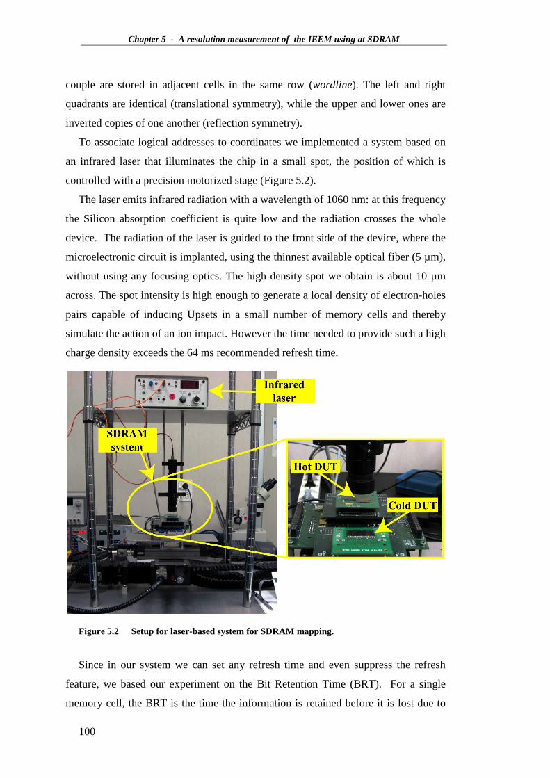
Chapter 5 - A resolution measurement of the IEEM using at SDRAM
100
couple are stored in adjacent cells in the same row (wordline). The left and right
quadrants are identical (translational symmetry), while the upper and lower ones are
inverted copies of one another (reflection symmetry).
To associate logical addresses to coordinates we implemented a system based on
an infrared laser that illuminates the chip in a small spot, the position of which is
controlled with a precision motorized stage (Figure 5.2).
The laser emits infrared radiation with a wavelength of 1060 nm: at this frequency
the Silicon absorption coefficient is quite low and the radiation crosses the whole
device. The radiation of the laser is guided to the front side of the device, where the
microelectronic circuit is implanted, using the thinnest available optical fiber (5 µm),
without using any focusing optics. The high density spot we obtain is about 10 µm
across. The spot intensity is high enough to generate a local density of electron-holes
pairs capable of inducing Upsets in a small number of memory cells and thereby
simulate the action of an ion impact. However the time needed to provide such a high
charge density exceeds the 64 ms recommended refresh time.
Figure 5.2 Setup for laser-based system for SDRAM mapping.
Since in our system we can set any refresh time and even suppress the refresh
feature, we based our experiment on the Bit Retention Time (BRT). For a single
memory cell, the BRT is the time the information is retained before it is lost due to

Chapter 5 - A resolution measurement of the IEEM using at SDRAM
101
the unavoidable charge leakage19. Once the memory refresh is inhibited, the cells
gradually lose their information, each cell with its own BRT (according to some
distribution). The effect of the laser is to significantly shorten the BRT of the cells
illuminated by the beam spot.
The experiment was performed by comparing the output of two identical
memories: one DUT was exposed to the laser spot (hot DUT); the other DUT was not
exposed (cold DUT). After a precise positioning of the hot chip with respect to the
optical fiber, the two twin memories were filled with a common logical value: '0000
0000'. The laser irradiation was applied for some seconds, before reading the
memories and comparing their outputs. The spatially contiguous cells illuminated by
the laser spot were observed as Upsets with consecutive addresses (a cluster).
In the areas located in the first half of each sector of the SDRAM (from row 0 to
row 255), the reconstructed map revealed the alternate presence of a pair of rows
sensitive to upsets, followed by a pair of insensitive rows. When we repeated the
measurement loading the memories with a logic pattern '1111 1111', we observed the
previously flipping cells now insensitive to the radiation, while the previously
insensitive cells underwent now to bit flips. Even though we do not know the detail
of the memory technology, we suppose that charged storage capacitors may be
discharged by the high density of free carriers generated by the ionizing radiation and
define positive logic the one in which a charged capacitor corresponds to a ‘1’ logic-
state and a discharged capacitor corresponds to a ‘0’ logic-state. We then can say
that, in these regions of the SDRAM, two consecutive rows are implemented in
19 To avoid losing any information, the SDRAM must be refreshed at time intervals inferior to the
BRT of the worst memory cell. The typical refresh time interval given by the manufacturer (64 ms)
ensures that no cell will lose information before the next refresh.

Chapter 5 - A resolution measurement of the IEEM using at SDRAM
102
positive logic, while the following two rows are implemented by negative logic. The
rest of each sector does not show this effect and we can assume that it is
implemented in negative logic (one in which a ‘0’, implemented as a charged
capacitor, may undergo a flip).
5.5 The SDRAM remapping
The laser experiment revealed that SDRAM implements a folded bit-line
architecture, as depicted in Figure 5.3.
Figure 5.5 represents the lower-half of quadrant 4: the sense amplifiers are placed
along the top; the memory array is subdivided into 12-by-16 subarrays (segments).
The surface of the SDRAM is not uniformly SEU-sensitive because the cells are
located exclusively inside the segments. Under visual inspection (optical
microscope) the segments appear as rectangles covered by equally spaced
metallization lines parallel to the vertical direction of the Columns (Figure 5.6),
while the cells are not visible
.
Figure 5.3 Folded bit-line architecture implemented our SDRAM: each sense amplifier
is connected to two parallel bit lines.

Chapter 5 - A resolution measurement of the IEEM using at SDRAM
103
Figure 5.4 The SDRAM chip layout. Chip size is 7.4 x 14.3 mm. The area in the dashed
rectangle is shown in detail in the following figure.

Chapter 5 - A resolution measurement of the IEEM using at SDRAM
104
Figure 5.5 SDRAM layout, detail of the dashed rectangle in the previous figure. The cells
Rows and Columns are organized in 12 x 16 segments. The area in the dashed rectangle is
shown in detail in the following figure.
Figure 5.6 Microphotograph of one detail of the SDRAM (the field of view is 165 by 135
µm): the picture shows the corners of two SDRAM segments and the 29 µm gap between
them.

Chapter 5 - A resolution measurement of the IEEM using at SDRAM
105
Most of the 12-by-16 segments have 86 lines (corresponding to 168 cells
columns), with the exception of the segments highlighted in Figure 5.7 (segment-
columns 3, 6, 9 and 12) which are a little bit larger and have 87 metallization lies
(corresponding to 176 cells columns). The horizontal and vertical gaps between the
segments are all 29 µm wide.
Figure 5.7 Detail of the SDRAM cells segments size and organization.
By dividing the 172 µm high segments by 256 rows, we obtain a row pitch of
0.336 µm, which is assumed to be the same in all segments. In the 168 columns wide
segments, the column pitch is 1.31 µm, while in the 176 columns segments, it’s a
little different: 1.35 µm.
The laser experiment revealed that the sensitive area of the SDRAM coincides
with the region below the metallization strips, but as the cells are not visible under
the optical microscope, we have to make an assumption on their position inside the
segment. The most reasonable assumption is that the Rows and Columns be straight,
each equally spaced and orthogonal, with the Column direction parallel with the
metallization lines observed in the segments and with the cells located at the
intersection points of the bit-lines and word-lines. However these working
assumptions, that might not reflect the real construction of the SDRAM, produce
negligible effects when compared with all the other uncertainties.

Chapter 5 - A resolution measurement of the IEEM using at SDRAM
106
5.6 SDRAM output file: data analysis
At this stage of the analysis we associate to the logical address of every upset
its physical location (remapping). Figure 5.8 show the upsets accumulated in a
sequence of 5 frames. One can observe the presence of 9 groups of upsets that are
interpreted as being due to 9 heavy ion impacts (in this case 241 MeV 79Br).
The next step is to implement a clustering algorithm to distinguish the groups of
upsets. The SDRAM is read row by row. The algorithm records the position of a
seed: the first upset it finds. The position of the next upset is compared with that of
the seed and the Pythagorean distance (dist2 = ∆x2 + ∆y2) is calculated. If the
distance is less than a maximum distance Dmax, the new upset it is associated to the
seed to form a cluster, otherwise the cluster of the seed is closed, the centroid of the
cluster is calculated and the new upset becomes a new seed. The process is repeated
till the end of file is reached.
1250
1270
1290
1310
1330
1350
1370
1390
1410
1430
1450
900 950 1000 1050 1100
X [microns]
Y [m
icro
ns]
Figure 5.8 The 41 upsets found in a sequence of 5 frames: nine groups are visible.
The maximum distance Dmax was set to 5 µm. This value was chosen looking at
the experimental event distribution not to arbitrarily mix separate clusters; for Dmax <
3 µm, the risk becomes high to break a single event in two clusters.

Chapter 5 - A resolution measurement of the IEEM using at SDRAM
107
Table 5.1 shows the result of the simple clustering algorithm of the upsets shown
in Figure 5.8. The first column gives the frame in which the upsets were found; the
second column is the progressive cluster number found by the algorithm; the third
column is the progressive number of the upset inside a cluster (the first is the seed of
the cluster); the 4th and 5th columns report the X and Y coordinates of the upsets. In
this case the algorithm correctly found all 9 groups.
Table 5.2 Table of the sequence of clustered upsets corresponding to Figure 5.8. In the
first column the cluster number, in the second the event number inside a cluster, then the X
and Y coordinate of the upset.
This simple clustering algorithm fails when two separate groups of upsets inside
the same SDRAM frame share a row (Figure 5.9); a distant upset on a row (B1)
becomes a new seed and breaks the clustering of the first group into two clusters
(clusters A and C). For the same reason even the second group is broken: the upsets
in the D cluster are not grouped properly with the B upsets. However only few events
fall in this category.

Chapter 5 - A resolution measurement of the IEEM using at SDRAM
108
Figure 5.10 Exemplification of how the simple clustering algorithm may fail. Upset C1 is
not grouped with cluster A while the cluster D is not grouped with cluster B.
5.7 Using the SDRAM to study the IEEM performance
5.7.1 Introduction
The high spatial regularity of the SDRAM makes it useful to measure the
effective lateral resolution of the IEEM and to map-out distortions in the IEEM
image. This is done by comparing the positions of the ion-induced SEU-clusters in
the memory array with the map of the ion impacts on the ultra-thin gold membrane
above the SDRAM as reconstructed by the IEEM.
We here report on a very high statistics experiment to measure the IEEM
performances. The experiment was made possible because of the important upgrades
to the SDRAM system:
1. the time-stamp is now available
2. the readout of the SDRAM can now be limited to any part of the memory
array, in particular to only that small portion that is exposed to the ion
beam and that that is the field of view of the IEEM.
Previously [54] the time-stamp was not implemented and the SDRAM readout
was very slow, as the whole memory was readout. For this reason a mechanical
shutter was used to inhibit the beam during the long readout process. The SDRAM
was exposed to a few tens of ions, during a short shutter-opening, as all the SEU
clusters in the exposure were then compared with the ion impacts registered by the
IEEM during the same exposure. This proof-of-principle experiment did give a first

Chapter 5 - A resolution measurement of the IEEM using at SDRAM
109
indication of the effective resolution of the IEEM setup, but the number of events
was too low to study image distortions.
In this experiment the 150×300 memory cells located in the 200 µm area exposed
to the ion beam are continuously read-out and refreshed at a frequency of 600 Hz and
the system looks for changes in the loaded logic pattern. In this way a temporal
coordinate can be assigned to every ion-induced upset cluster with an accuracy of
~1.7 ms, the readout period of the portion of the SDRAM exposed to the ion beam.
The ions are detected by the IEEM system as they passes through the Au-Si3N4
membrane and the spatial and temporal coordinates of the impact point are recorded;
the events collected by the SDRAM system and by the IEEM are put into correlation
employing the time-stamp coordinates associated to each event. This analysis is
performed offline, by comparing the files generated by the two systems. The readout
period of the IEEM system is 17 times faster than the SDRAM one (the temporal
accuracy of the IEEM system is 106 µs). Therefore every SDRAM centroid is
associated with all the IEEM events detected up to 1.7 ms earlier. In this experiment
the ion flux (106 cm-2 s-1) was high to accumulate enough statistics. With this flux 3–
5 IEEM events, on average, were associated with every SDRAM readout, only one
of which may correspond to the ion that created a SDRAM cluster. Some of the
additional events were beam-related background signals in the IEEM system, not due
to real ion impacts on the SDRAM20.
5.7.2 A high statistics experiment using 241 MeV Br79 ions
In this high statistics experiment we used a 241 MeV 79Br ion beam, collecting
240,000 events (fluence of 109 cm-2), a number that allows us to evaluate the quality
of the image generated by the IEEM in a way not previously possible. The distance
of the SDRAM from the Au-Si3N4 membrane was comfortably adjusted to 800 µm,
which we consider a large distance, almost a worst-case scenario. This choice is due
to the presence of contact pads for the wire bonds located at the middle of the
SDRAM. The ion flux of this experiment was ∼500 ions/s in the field of view.
20 These background signals is now reduced by placing a 500 µm collimator 1 m upstream of the
MCP of the IEEM. The background suppressing collimator, now a standard feature, was not available
at the time of the experiment here described.
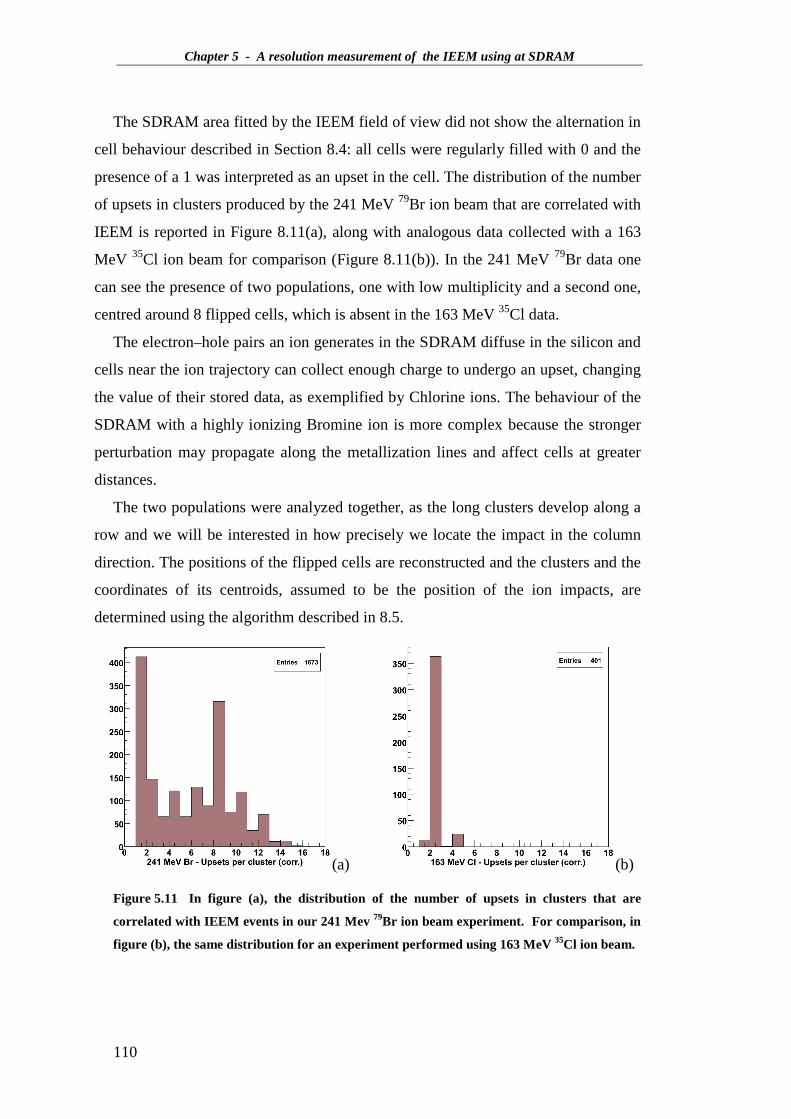
Chapter 5 - A resolution measurement of the IEEM using at SDRAM
110
The SDRAM area fitted by the IEEM field of view did not show the alternation in
cell behaviour described in Section 8.4: all cells were regularly filled with 0 and the
presence of a 1 was interpreted as an upset in the cell. The distribution of the number
of upsets in clusters produced by the 241 MeV 79Br ion beam that are correlated with
IEEM is reported in Figure 8.11(a), along with analogous data collected with a 163
MeV 35Cl ion beam for comparison (Figure 8.11(b)). In the 241 MeV 79Br data one
can see the presence of two populations, one with low multiplicity and a second one,
centred around 8 flipped cells, which is absent in the 163 MeV 35Cl data.
The electron–hole pairs an ion generates in the SDRAM diffuse in the silicon and
cells near the ion trajectory can collect enough charge to undergo an upset, changing
the value of their stored data, as exemplified by Chlorine ions. The behaviour of the
SDRAM with a highly ionizing Bromine ion is more complex because the stronger
perturbation may propagate along the metallization lines and affect cells at greater
distances.
The two populations were analyzed together, as the long clusters develop along a
row and we will be interested in how precisely we locate the impact in the column
direction. The positions of the flipped cells are reconstructed and the clusters and the
coordinates of its centroids, assumed to be the position of the ion impacts, are
determined using the algorithm described in 8.5.
(a) (b)
Figure 5.11 In figure (a), the distribution of the number of upsets in clusters that are
correlated with IEEM events in our 241 Mev 79Br ion beam experiment. For comparison, in
figure (b), the same distribution for an experiment performed using 163 MeV 35Cl ion beam.

Chapter 5 - A resolution measurement of the IEEM using at SDRAM
111
Figure 5.12 shows the coordinates of the SEU found in the SDRAM in this
experiment. Most of the SEU are located inside the 200 µm diameter disc given by
the contrast diaphragm of the IEEM. The empty crossed region inside the disc is due
to the absence of memory cells outside the array segments; in this region run the data
connection lines of the SDRAM. The points outside and far from the disc are due to
occasional corruptions of addresses.
Figure 5.12 The SEU locations as reconstructed by the mapping. The locations outside the
disc-like region (the exposed area) are due to the corruption of the address of upset cells.
The clustering algorithm is now employed to calculate the centroid of the SEU-
clusters (Figure 5.13). The centroid is assumed to be the position of the ion impact on
the SDRAM.
For the following discussion, it is important to keep in mind that the centroid is
determined with a better uncertainty in the Y-direction as the distance of the rows of
the memory cells (Y-direction) is 0.3 µm, while the distance of the columns (X-
direction) is 0.6 µm. However the cells of the array are organized in pairs of bits that

Chapter 5 - A resolution measurement of the IEEM using at SDRAM
112
occupy the same row and two adjacent columns. When we detect a SEU of only one
cell of a pair, we cannot establish with certainty the column of the flipped cell, so we
decided to map the X-coordinate of a bit flip at the center of the cell-pair21. With this
choice the granularity of the X-coordinate is 1.2 µm. For this reason the resolution
studies and results we report will always refer to the Y-coordinate.
Figure 5.14 The centroids calculated by the clustering algorithm. The centroid is taken to
be the ion impact point as detected by the SDRAM. These points will be then compared to
the ion impact points on the gold membrane ad reconstructed by STRIDE.
Figure 5.15 shows the ion impact points on the ultra-thin gold membrane as
reconstructed by the IEEM. Most of the points are distributed in a roughly annular
region: the central region corresponds to the hole of the annular MCP secondary
electron detector. The otherwise scattered points (including the ones inside the
central region) are due to occasional errors in determining one or both the impact
coordinates. 21 This ambiguity could not be resolved with the laser remapping technique because the laser spot
was too big (∼10 µm).

Chapter 5 - A resolution measurement of the IEEM using at SDRAM
113
Figure 5.15 The ion impact points on the ultra-thin gold membrane as reconstructed by the
IEEM. Most of the points are distributed in a roughly annular region: the central region
corresponds to the hole of the annular MCP secondary electron detector. The scattered
points (including the ones inside the central region) are due to occasional errors in
determining the impact coordinates.
The present STRIDE algorithm makes errors when:
1. STRIDE matches the X-coordinate of one event with the Y-coordinate of
the preceding or the following event. This may occur when the ion
detection rate is high, as in this high statistics experiment.
2. when two ion impact events are recorded in the same frame. In this case
the X and Y ambiguity may only be resolved if the two signals have a
different amplitude. These errors occur easily when the ion impact is near
the edge of the field of view since the amplitude of the near-edge signal is
suppressed by the optical system (aberrations);
3. a real signal on one coordinate is matched with a noise signal.

Chapter 5 - A resolution measurement of the IEEM using at SDRAM
114
5.7.3 IEEM-SDRAM Data Correlation
We now present the results of the data analysis that matches the ion impacts
detected by the IEEM and by the SDRAM.
The SDRAM centroids and the IEEM detected impacts are put into correlation by
employing the time coordinate associated to each event. To readout the irradiated
area of the SDRAM typically takes about 17 FrameNumbers, which corresponds to a
1.7 ms readout time. The time correlation between SDRAM and STRIDE events is
performed in this time interval in the following way: the time coordinate of a
SDRAM cluster is the FrameNumber in which it was detected; all the STRIDE
events that that occurred in the 1.7 ms time interval prior to that FrameNumber are
associated to the cluster. Figure 5.16 shows a SDRAM centroid (red circle) and four
STRIDE events (blue dots) that preceded it within 1.7 ms.
The time information is therefore not sufficient to unambiguously associate a
SDRAM event with a STRIDE one. The ambiguity can be resolved by requiring
spatial proximity. In Figure 5.16 the IEEM signal that lies within the 4 µm radius
circle centred around the SDRAM fired cell is likely to be due to the ion that caused
the upset in the SDRAM.
However a circular proximity cut is meaningless to measure the spatial resolution
of the IEEM. Instead a Transverse Cut is applied in the following by requiring the
difference of the X-coordinates (the less precise ones) of the STRIDE event and of
the SDRAM centroid to be less than 10 µm.
Figure 5.17 shows a set of nine SDRAM centroids in a 50×50 µm2 region and the
STRIDE events that are correlated temporally and accepted by the Transverse Cut: 6
out of 9 centroids have a STRIDE event nearby.

Chapter 5 - A resolution measurement of the IEEM using at SDRAM
115
Figure 5.16 The red circle is centred at the position of the centroid of one SDRAM cluster.
The blue dots are IEEM events that are temporally associated to it. The radius of the red
circle is 4 µm.
-40
-30
-20
-10
0
10
0 10 20 30 40 50
X [µm]
Y [
µm]
Figure 5.17 The red circles of radius 4 µm are centred at the positions of the centroid of
SDRAM clusters and the IEEM events (blue dots) that are temporally associated to them. In
addition the Transverse cut (see text) is applied to impose a proximity requirement.
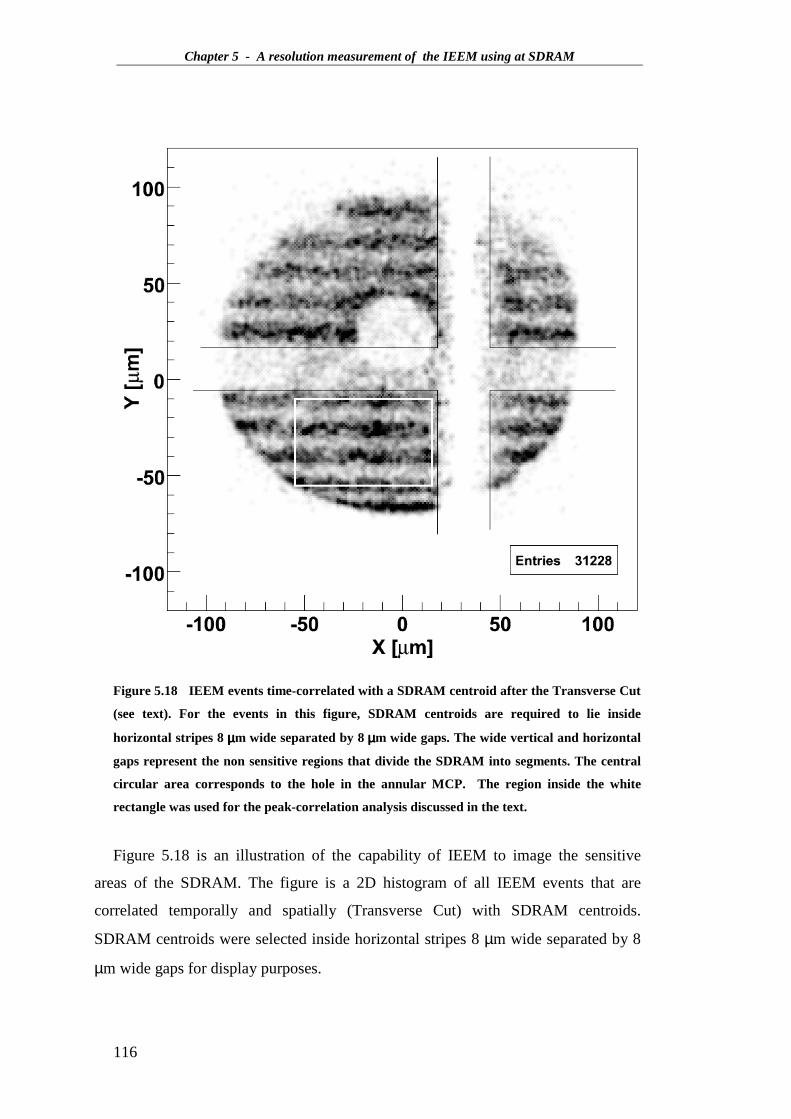
Chapter 5 - A resolution measurement of the IEEM using at SDRAM
116
Figure 5.18 IEEM events time-correlated with a SDRAM centroid after the Transverse Cut
(see text). For the events in this figure, SDRAM centroids are required to lie inside
horizontal stripes 8 µ µ µ µm wide separated by 8 µ µ µ µm wide gaps. The wide vertical and horizontal
gaps represent the non sensitive regions that divide the SDRAM into segments. The central
circular area corresponds to the hole in the annular MCP. The region inside the white
rectangle was used for the peak-correlation analysis discussed in the text.
Figure 5.18 is an illustration of the capability of IEEM to image the sensitive
areas of the SDRAM. The figure is a 2D histogram of all IEEM events that are
correlated temporally and spatially (Transverse Cut) with SDRAM centroids.
SDRAM centroids were selected inside horizontal stripes 8 µm wide separated by 8
µm wide gaps for display purposes.

Chapter 5 - A resolution measurement of the IEEM using at SDRAM
117
Figure 5.19 The experimental correlation peak distribution for the events lying in regions I
and II shown Figure 5.18.
We measured the resolution of the IEEM with the correlation-peak technique [54]
which consists in filling a histogram of the Y-coordinate difference of every
SDRAM centroid with all the IEEM events accepted by time correlation and the
Transverse Cut. Only the events within the 45 µm-by-70 µm fiducial region of Figure
5.18 were considered in the analysis.
The histogram, shown in Figure 5.19, presents a Gaussian shaped correlation peak
(σ = 2.8 ± 0.1 µm, corresponding to FWHM = 6.6 ± 0.2 µm) above a quadratic
combinatorial background. The error we report is the spread of the values of the

Chapter 5 - A resolution measurement of the IEEM using at SDRAM
118
sigmas we obtained performing the analysis in 4 equal regions obtained by dividing
the white rectangle into 4 equal parts.
The correlation-peak signal above background is due the successful matching of
STRIDE events with SDRAM centroid and the width of the peak is taken to be the
measure of the spatial resolution of the IEEM.
In spite of the high statistics this experiment does not improve the preliminary
resolution measurement reported in the previous work [54]. This unsatisfactory
outcome, in spite of the improvement in the experimental apparatus and the high
collected statistics, deserves to be carefully studied. Some results of this study will be
reported in the following chapter. We only recall here some experimental differences
between this and the previous experiment and we make explicit an assumption.
1. the distance of the SDRAM from the gold membrane (now 800 µm) was
previously 300 µm only;
2. two different SDRAMs were used in the two experiments;
3. the two SDRAMs were not irradiated in the same specific area but these
were arbitrarily chosen;
5.7.4 Efficiency of the IEEM system in reconstructing ion
impacts
Not all of the SDRAM centroids can be detected by the IEEM. The main sources
of inefficiencies of the IEEM are:
• the field of view of STRIDE (diameter 180 µm) is smaller than the
irradiated area (diameter 200 µm);
• the annular MCP is geometrically inefficient (central hole; blind spots);
• the biasing wire of the diaphragm of the annular MCP casts a shadow;
• the inefficient detection of secondary electrons (the MCP was not at full
voltage22);
22 The annular MCP is showing signs of age. To slow aging and avoid the formation of new blind
spots we set the working voltage at 4.8 kV instead of the nominal 5.0 kV.

Chapter 5 - A resolution measurement of the IEEM using at SDRAM
119
• the inefficiency of the image intensifier in detecting photons created by the
MCP+phosphor stack inside the IEEM;
• the measurements errors of STRIDES.
To evaluate the efficiency of the IEEM system to correctly reconstruct ion
impacts we calculated the fraction of times a STRIDE event is successfully
associated with a SDRAM centroid respect to the total number of SDRAM centroids.
The region we used is the fiducial region shown in Figure 5.18; it was chosen as it is:
• away from the gaps between the segments of the SDRAM;
• away from the central hole of the annular MCP and other inefficient areas
of the MCP;
• away from the shadow of the biasing wire.
A total number of 12452 SDRAM centroids are inside the fiducial region. The
number of correlated STRIDE events, in this case 7607, is determined by the number
of entries under the correlation-peak, i.e. the area of its gaussian fit. The measured
effective efficiency of reconstructing the ion impact and associating it to a SDRAM
cluster is hence measured to be 61%, instead of the previously reported ∼90% [55]. It
is the net effect of the degradation in efficiency of:
1. the annular MCP inside the IEEM in detecting the secondary electrons
emitted by the ion impacts on the ultra-thin gold membrane;
2. the image intensifier in detecting photons from the MCP+phosphor stack
of the IEEM;
3. the NMOS sensors;
4. the STRIDE system in correctly reconstructing the ion impact positions in
a high statistics experiment.
We do not worry about the loss in efficiency which is essentially a money
problem.


Chapter 6 - Resolution degradation studies
121
6 Resolution degradation studies
The resolution of the IEEM system at SIRAD (σ=2.8±0.1 µm) appears to be at
least two times worse than the one reported by Doyle [6]. We note that also the
resolution using UV photo-electrons (the PEEM mode) is worse than the one
reported by the manufacturer (see 4.2.2).
The global IEEM performance can be affected by many factors:
1. the presence of image distortions in the field of view (FOV);
2. the scattering of the ions crossing the gold-Si3N4 membrane;
3. the presence of vibrations in the IEEM system;
In this chapter we will take advantage of the high statistics collected in the BR
experiment, which was not available in the previous ones, to try to disentangle the
different factors that can affect our spatial resolution. In addition we will describe
two studies we performed to investigate the discrepancy of the resolution of the
PEEM/IEEM system: a study of the vibrations and a study of the output signals of
the light sensor of the DAQ.
6.1 Evaluation of the factors affecting the resolution
The analysis reported in this section is based on the events collected with the 241
MeV 79Br ion beam discussed in the previous chapter.
To study large scale distortions across different regions of the full field of view,
we divided it into 10×10 µm2 areas and performed in each the correlation-peak
analysis to measure the resolution in the Y-direction. Figure 6.1 shows the
distribution of the differences among the means of the correlation peaks calculated in
the single small size areas and their global average: for more than 90% of the areas
the difference is less than 2 µm. Some systematic effects are present as outlined by
the 2D distribution of the means of the correlation peaks shown in Figure 6.2. In this

Chapter 6 - Resolution degradation studies
122
figure the size of each marker is proportional to the difference from the global
average; the sign of the difference is encoded by the grey intensity
Figure 6.1 Distribution of the differences from the average value of the means of the Y-
coordinate correlation peaks in the 10x10 µm2 areas of Figure 6.2.
Figure 6.2 2D histogram of the means of the correlation peaks in the Y-coordinate in the
10×10 µm2 areas of the central region on the field of view. The size of each marker is

Chapter 6 - Resolution degradation studies
123
proportional to the difference from the global average; the sign of the difference is encoded
by the grey intensity.
Nevertheless the histogram of the sigmas of such distributions is Gaussian (Figure
6.3) with an average value (average local resolution) σave = 2.81 ± 0.38 µm. The
spatial resolutions calculated on small size areas do not disagree with the global one,
indicating that, although distortions are present and may be corrected, they are not
the major factor in degrading the spatial resolution of our IEEM.
To simulate the effects of the membrane (a 30 nm layer of gold on a 100 nm layer
of Si3N4) on 240 MeV 79Br ions we used the SRIM [63] code. In our simulation the
ion direction is orthogonal to the membrane surface and ions are uniformly
distributed within the fiducial box of Figure 8.19. The SRIM output file was used to
project the scattered ions onto a parallel plane 800 µm away (the distance between
membrane and SDRAM in the experiment). The two sets of the ion impact
coordinates (on the surface of the membrane and on the distant parallel plane) were
then analyzed with the correlation-peak technique. The correlation peak in the Y-
coordinate is slightly non-Gaussian (10% of events are not accounted for by a
Gaussian distribution with σ = 0.86 µm) over a small combinatorial background
(Figure 6.4 (a)). In any case we can conclude that the scattering of the ions on the
membrane is not the factor that affects most our experimental spatial resolution.
Figure 6.3 Distribution of the sigmas of the Y-coordinate correlation peaks in the 10x10
µm2 areas of Figure 6.2.

Chapter 6 - Resolution degradation studies
124
Figure 6.4 (a) Correlation peak (in log scale) of SRIM simulated data (240 MeV 79Br)
broadened only by the scattering due to the membrane (membrane contribution): the peak is
slightly non-Gaussian. (b) The above SRIM distribution convoluted with a Gaussian (the fit
is a Gaussian plus a quadratic background).
All other resolution degradation effects (for example: vibrations, STRIDE re-
construction errors, …) can be collectively accounted for by performing a
convolution of the scattering effect of the membrane reported above with a Gaussian
distribution: the X and Y coordinates of the simulated SRIM scattered events were
further randomly scattered with a Gaussian probability distribution function, of zero
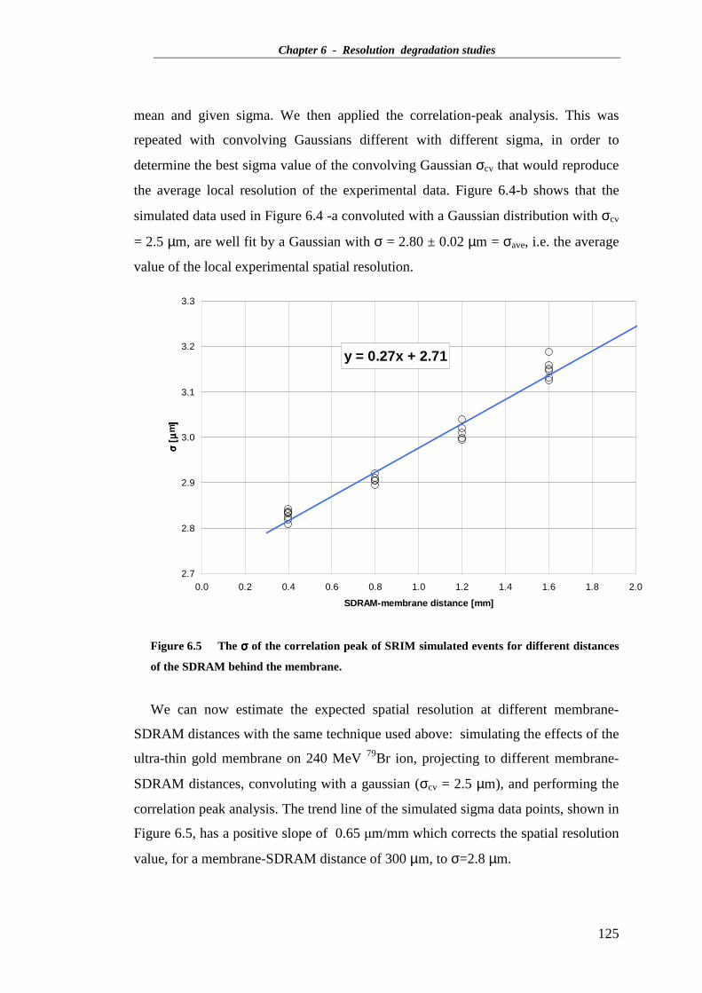
Chapter 6 - Resolution degradation studies
125
mean and given sigma. We then applied the correlation-peak analysis. This was
repeated with convolving Gaussians different with different sigma, in order to
determine the best sigma value of the convolving Gaussian σcv that would reproduce
the average local resolution of the experimental data. Figure 6.4-b shows that the
simulated data used in Figure 6.4 -a convoluted with a Gaussian distribution with σcv
= 2.5 µm, are well fit by a Gaussian with σ = 2.80 ± 0.02 µm = σave, i.e. the average
value of the local experimental spatial resolution.
y = 0.27x + 2.71
2.7
2.8
2.9
3.0
3.1
3.2
3.3
0.0 0.2 0.4 0.6 0.8 1.0 1.2 1.4 1.6 1.8 2.0
SDRAM-membrane distance [mm]
σ [
µ σ
[µ
σ [
µ σ
[µ
m]] ]]
Figure 6.5 The σσσσ of the correlation peak of SRIM simulated events for different distances
of the SDRAM behind the membrane.
We can now estimate the expected spatial resolution at different membrane-
SDRAM distances with the same technique used above: simulating the effects of the
ultra-thin gold membrane on 240 MeV 79Br ion, projecting to different membrane-
SDRAM distances, convoluting with a gaussian (σcv = 2.5 µm), and performing the
correlation peak analysis. The trend line of the simulated sigma data points, shown in
Figure 6.5, has a positive slope of 0.65 µm/mm which corrects the spatial resolution
value, for a membrane-SDRAM distance of 300 µm, to σ=2.8 µm.

Chapter 6 - Resolution degradation studies
126
This result confirms that the spatial resolution is practically insensitive to the
SDRAM-membrane distance, below 1 mm, and that it is dominated by other factors.
A study of the vibrations of the IEEM system
Vibrations could be one of the principal causes of the resolution degradation.
Indeed we did not invest great efforts to ensure a vibration-free platform, but simply
decoupled the IEEM from the vacuum pumps by means of a rubber damper.
To answer to this issue we used an accelerometer (PCB Piezotronics, model
352B10) to measure the vibration of key parts of the IEEM which could be afflicted
by this problem.
The first element of the IEEM system we suspected to be prone to vibration
problems was the PEEM itself (Figure 6.6), since it is a heavy horizontal metal
cylinder mounted as a cantilever with only one full moment connection (the
restrained end keeps the PEEM from rotating in the vertical plane; from falling). The
accelerometer was mounted on the side of the cylinder, as close as possible to the
free tip of the PEEM, with the axis in vertical position.
Figure 6.6 Schematic of the PEEM (shadowed in grey) anchored to the IEEM vacuum
chamber.

Chapter 6 - Resolution degradation studies
127
A low noise signal conditioner (PCB Piezotronics, model 482A22) was used to
power the accelerometer and to condition the measured signal for a spectrum
analyzer (Stanford Research Systems SR770 FFT network analyzer). The analyzer
displays the square root of the Power Spectral Density (√PSD) of the voltage output
signal expressed in V/√Hz. The analysis of the PSD immediately reveals the
dominant vibration frequencies, allowing the fast identification of the frequency of a
particular vibration source. Once identified, a source could be switched off or the
disturbance minimized, for example by moving it away. We expected the vacuum
pumps to be the main causes of vibrations and this study was intended to be just the
starting point for the elaboration of a strategy to minimize its amplitude as the pumps
cannot be shut off or removed during IEEM operations.
The presence of characteristic harmonics in the vibration spectrum of the PEEM
was quickly verified by simply knocking on the vacuum chamber (Figure 6.6). A set
of power peaks appeared in the 300−750 frequency band, together with an excitation
peak centred on 1.69 kHz and another one at a lower frequency, centred on 58 Hz.
In particular the 58 Hz peak was very susceptible to excitation when the flange
holding the PEEM was slightly tapped (Figure 6.7).
0.00E+00
5.00E-06
1.00E-05
1.50E-05
2.00E-05
2.50E-05
000.0E+0 500.0E+0 1.0E+3 1.5E+3 2.0E+3 2.5E+3 3.0E+3
Freq. [Hz]
Acc
el.O
ut [V
/Sqr
t(H
z)]
Knocking
bkg
Figure 6.6 The plot shows the square root of the power spectral density of the output
signal of the accelerometer placed on the tip of the PEEM. The blue line is the vibrational
spectrum of the PEEM by simply knocking on the vacuum chamber; in red the background.

Chapter 6 - Resolution degradation studies
128
0.00E+00
5.00E-05
1.00E-04
1.50E-04
2.00E-04
2.50E-04
0 50 100 150 200 250 300 350 400Freq. [Hz]
Acc
el.O
ut [u
V/S
qrt(
Hz)
]free
Tipping
Figure 6.7 In blue the vibration spectrum of the PEEM in the low frequency region. In
blue the 58 Hz peak is excited by lightly tapping on the flange of the PEEM; in red the
background.
0.00E+00
2.00E-06
4.00E-06
6.00E-06
8.00E-06
1.00E-05
1.20E-05
1.40E-05
0 50 100 150 200 250 300 350 400
Freq. [Hz]
Acc
el.O
ut [u
V/S
qrt(
Hz)
]
free
Damped
Figure 6.8 In blue the power spectral density of the vibration of the PEEM perturbed
tightening the tip with a hand; in red the PEEM free to vibrate.

Chapter 6 - Resolution degradation studies
129
0.0E+00
2.0E-06
4.0E-06
6.0E-06
8.0E-06
1.0E-05
1.2E-05
1.4E-05
0 500 1000 1500 2000 2500 3000Freq. [Hz]
Acc
el.O
ut [V
/Sqr
t(H
z)]
bkg
Scroll ON
Scroll ON / bkg
Figure 6.9 Contribution to the vibrations due to the scroll pump: in red the vibration
power spectrum with the scroll pump on (signal), in blue the pump is off (background). In
green the ratio of the signal and the background (multiplied by a factor 10^-5 to fit the plot).
Figure 6.8 shows in red the power spectrum in the lower frequency band (0-390
Hz): peaks near 50 and 60 Hz and their multiples are evident. We believe these
peaks are artefacts caused by the power stage of the spectrum analyzer. To check
this we firmly held with a hand the tip of the PEEM (the blue spectrum): all the
peaks remain unchanged, with the exception of the 58 Hz peak, which now appears
lower and broadened. This confirmed the existence of a true vibration mode with a
frequency of 58 Hz that affects the PEEM even when no external perturbation is
exerted. In this acquisition, both the scroll and the turbomolecular pumps of the
IEEM and all the other sources of vibration that are under our direct control were
inactive; i.e. other vacuum pumps on the SIRAD beam line were turned off while
pumps on other beam lines in the experimental hall were not.

Chapter 6 - Resolution degradation studies
130
0.00E+00
2.00E-06
4.00E-06
6.00E-06
8.00E-06
1.00E-05
1.20E-05
1.40E-05
300 1300 2300 3300 4300Freq. [Hz]
Acc
el.O
ut [V
/Sqr
t(H
z)]
bkg
Pump
Figure 6.10 Contribution to the vibrations due to the turbomolecular pump: in red the
vibration power spectrum with the scroll pump on only, in blue both the scroll and the
turbomolecular pumps are running at top speed.
We then measured the contribution to vibrations given by the IEEM vacuum
pumps. Figure 6.9 shows in blue the power spectral density of the signal of the
accelerometer when the scroll pump is ON, in red the same signal with pump OFF.
For clarity the ratio between the two lines is reported in green (multiplied by a factor
10-5 to fit the plot), showing no meaningful contribution to the vibration spectrum23.
Similarly, we found no evidence of contributions coming from the turbomolecular
pump (Figure 6.10) which, working at a frequency of 700 Hz, was expected to excite
high frequency vibrations.
A rough estimate of the amplitudes of the vibrations can be made by modelling
our system as an harmonic oscillator: the rms amplitude of the vibration (V) increases
linearly with the rms amplitude of the impressed acceleration (A) and is inversely
proportional to the square root of the frequency (f )
(6.1) Af
V ⋅=224
1
π
23 To show that there is no significant difference between the two cases (pumps ON/OFF), we did
not consider the simple difference of the spectra because it is not meaningful to subtract two noise
spectra to look for a signal that is smaller than the noise.

Chapter 6 - Resolution degradation studies
131
In our case, the dominant vibration mode has an amplitude of ~10 µV/√Hz rms,
that corresponds to an acceleration of 10-3 g/√Hz rms (1 g = 9.81 m/s2), integrated
over the width of the power peak: a 1 Hz frequency band (the binning of the PSD
output). With this data we calculate a vibration amplitude of ~70 nm rms which is
more than an order of magnitude smaller than the actual measured resolution of our
PEEM with UV photons, and 7 times smaller than the resolving power featured by
the PEEM in ideal conditions (manufacture’s specs).
These first measurements suggest that the main limiting factor of the system
resolution is not due to the PEEM vibrations.
The second element we suspected was the holder of the Device Under Test, a
complex micrometric-precision motorized stage; i.e. the holder is not a mono-block
but is made of movable parts. For these measurements we built a dummy aluminium
DUT provided with a notch on one side to host the accelerometer. The accelerometer
was mounted on the upper face of the dummy DUT with the axis in the vertical
position to give a measurement of the vertical component of the acceleration.
An analogous analysis performed on the sample holder found no evidence of
excited proper oscillation modes.
To support this conclusion, we chose to artificially excite the 58 Hz vibration
mode of the PEEM and measured the consequent image degradation as a function of
the induced vibration amplitude.
To excite the vibration we used a vibrational exciter (Brüel & Kjær, type 4308)
placed on the floor that pushes up on the base of the frame that holds onto the base of
the mechanical support of the IEEM system (Figure 6.11). The exciter was powered
by an amplifier (Brüel & Kjær, type 2712) driven by a 58 Hz sinusoidal voltage
signal, provided by a function generator. Figure 6.12 shows the amplitude of the
power frequency spectrum of the 58 Hz peak (expressed in V/√Hz) as a function of
the amplitude of the driving voltage of the excitation. The red dot represents the
amplitude of the vibration of the PEEM when no controlled excitation is provided.
The blue diamonds show the linear regime of the excitation response (a linear fit in
lighter blue), while the green diamonds show the non-linear regime of the response
for a more intense excitation.
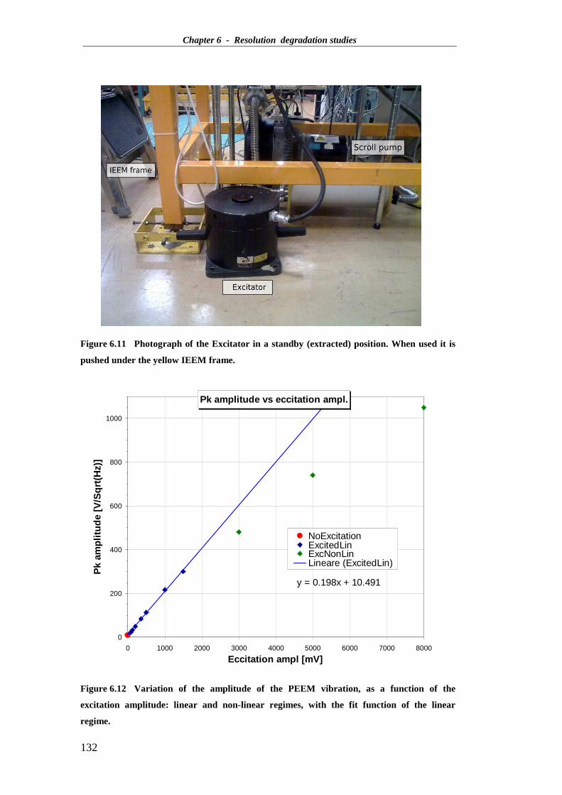
Chapter 6 - Resolution degradation studies
132
Figure 6.11 Photograph of the Excitator in a standby (extracted) position. When used it is
pushed under the yellow IEEM frame.
Pk amplitude vs eccitation ampl.
y = 0.198x + 10.491
0
200
400
600
800
1000
0 1000 2000 3000 4000 5000 6000 7000 8000
Eccitation ampl [mV]
Pk
ampl
itude
[V/S
qrt(
Hz)
]
NoExcitationExcitedLinExcNonLinLineare (ExcitedLin)
Figure 6.12 Variation of the amplitude of the PEEM vibration, as a function of the
excitation amplitude: linear and non-linear regimes, with the fit function of the linear
regime.

Chapter 6 - Resolution degradation studies
133
To analyze the dependence of the PEEM resolution as a function of the vibration
amplitude, we took several images of a constellation of bright spots located on the
non-emitting surface of the PEEM reference target.
We first accurately focused the system by acquiring a series of four images,
setting slightly different voltage values in the objective lens (1.230; 1.235; 1.240;
1.250 kV) and choose the condition providing the best resolved image (following
table):
IEEM focus condition
VTransfer 10.00 kV VProjective B 0.21 kV
VObjective 1.205 kV VDecel 1 kV
V Intermediate 9.98 kV MCP voltage 5 kV
VProjective A 7.03 kV Image Intens. gain 5 V
Figure 6.13 The constellations of emitting spots in three different conditions: A) no excited
vibrations; B) natural vibration increased by a factor 45: twofold worst resolution; C)
excited vibration at full scale: the tip of the PEEM is actually turning around in a circle.
Once the PEEM optics was adjusted, we activated the mechanical excitator to
increase the amplitude of the 58 Hz proper vibration of the PEEM and acquired new
images (Figure 6.13). In the hypothesis that the dominant contribution to the
degradation of the resolution of the IEEM was due to this vibration power peak, we
expected to see a blurring of the imaged spot when the external excitation was active,
proportional to the amplitude of the vibration. To measure this effect, we analyzed
the imaged spots by projecting them along the X axis (Figure 6.14) and by fitting this

Chapter 6 - Resolution degradation studies
134
projection with a gaussian function. Figure 6.15 shows the plot of the gaussian fit
sigma versus the excitation amplitude (in reality the ratio of both variables to the
value when no external perturbation was applied).
Figure 6.14 On the left: IEEM image of a constellation of small electron-emitting spots in a
non-emitting background (arbitrary units). On the right the horizontal projection of the
spot C with a gaussian fit.
A slight improvement of the resolution is visible when the external excitation is
activated; this could be due to a settlement of the target carrier, caused by the
vibration itself, that slightly varied its distance from the microscope, resulting in a
drift of the focus condition. This effect doesn’t affect the conclusion of the
measurements that show that even if we increase by one order of magnitude the
proper PEEM vibration, no meaningful increase of the spots blurring was observed.
To obtain a twofold blurring increase, we had to rise the PEEM vibration of a factor
45, reaching a vibration amplitude of ~3 µm rms.

Chapter 6 - Resolution degradation studies
135
0.00
0.50
1.00
1.50
2.00
2.50
0 5 10 15 20 25 30 35 40 45 50Relative vibration
Rel
ativ
e si
gma
relative A spread
relative B spread
relative C spread
Figure 6.15 Relative variation of the gaussian sigma of the three imaged points (relative
to the condition without excitation) as a function of the relative amplitude of the exerted
excitation (relative to the proper vibration amplitude). The error along the Y axis is of the
order of 1%.. The points are joined with segments to guide the eye.
We conclude that the IEEM system does vibrate at 58 Hz but the amplitude of
vibration is too small to account for the discrepancy between the PEEM resolution
we obtain and the nominal one reported by the manufacturer. The PEEM has been
sent back to the producer for refitting.
Any way vibrations are not at the origin of the unsatisfactory spatial resolution we
found in the IEEM mode.
A study of the signal profile of the NMOS sensors
We then analyzed whether the algorithms used by STIDE to provide the
coordinates of the ion impact points may introduce some errors due to differences
between the real and the expected luminous signals converted in electric signals by
the NMOS sensors.
The experiment was performed with the UV source (IEEM in the PEEM mode)
since no more ion beam was available and STRIDE does not record the shapes of the
luminous signals but only the calculated charge centroids. Actually an inspection of

Chapter 6 - Resolution degradation studies
136
the pixel outputs of individual events (single shot acquisitions) present asymmetric
peaks in many events.
Figure 6.16 The X- and Y-coordinate pixel profiles of a UV event that is slightly
asymmetric in both X (top) and Y (bottom) coordinates. The position detection algorithm of
STRIDE uses only pixels above threshold (16 units on the vertical axis) so in this case the
algorithm sees a symmetric pixel distribution.
Figure 6.16 shows the pixel output of the NMOS sensors of STRIDE and
represents the impact of a UV photo-electron. In this case the pixel profile of the
event is slightly asymmetric in both X (top) and Y (bottom) coordinates. However,
when the position detection algorithm of STRIDE calculates the centroid (weighted
mean) of the peaks, it uses only pixels above threshold (16 units on the vertical axis).
Hence in this case the algorithm sees symmetric pixel distributions and the centroids
coincide with the positions of the maxima of the peaks.
Figure 6.17 shows the X-coordinate pixel profile of two distinct UV-events in the
same portion of the NMOS sensor. In this case the position detection algorithm sees
the asymmetry of the first event even above threshold (manifest asymmetry).
Asymmetric peaks are very frequent (about 40% of the total) and are distributed
somewhat uniformly. It is important to note that the asymmetry does not depend on
the X-coordinate.
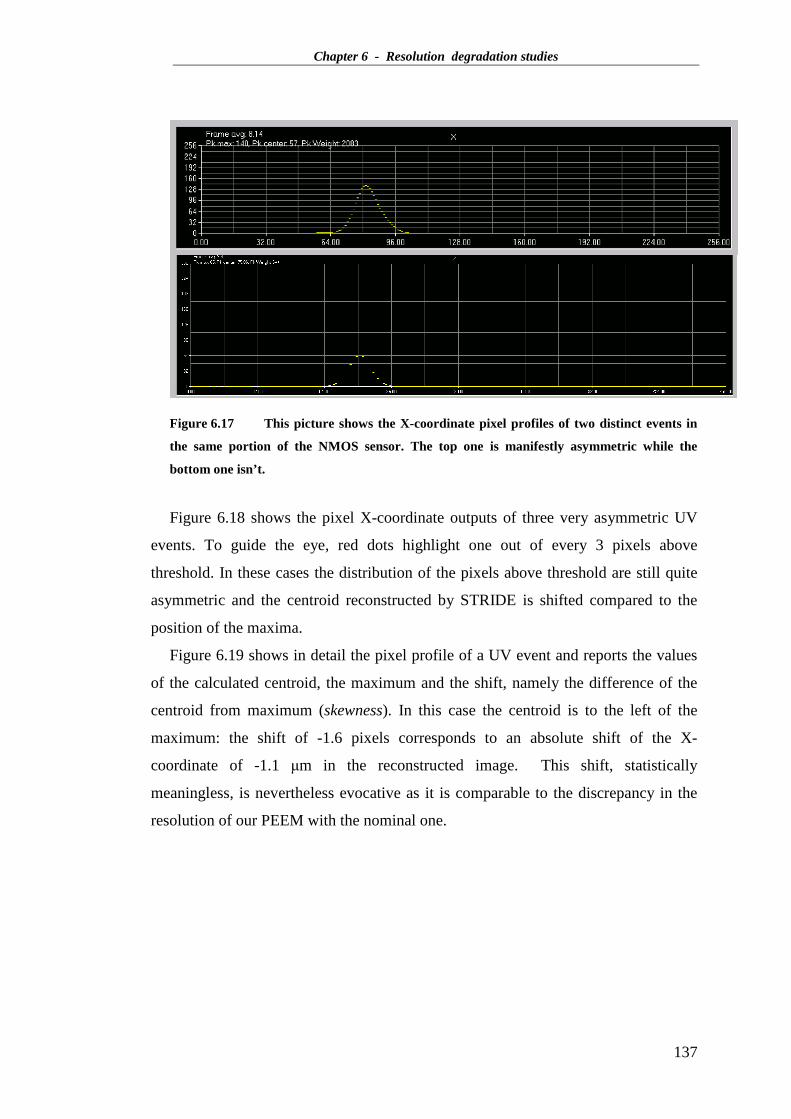
Chapter 6 - Resolution degradation studies
137
Figure 6.17 This picture shows the X-coordinate pixel profiles of two distinct events in
the same portion of the NMOS sensor. The top one is manifestly asymmetric while the
bottom one isn’t.
Figure 6.18 shows the pixel X-coordinate outputs of three very asymmetric UV
events. To guide the eye, red dots highlight one out of every 3 pixels above
threshold. In these cases the distribution of the pixels above threshold are still quite
asymmetric and the centroid reconstructed by STRIDE is shifted compared to the
position of the maxima.
Figure 6.19 shows in detail the pixel profile of a UV event and reports the values
of the calculated centroid, the maximum and the shift, namely the difference of the
centroid from maximum (skewness). In this case the centroid is to the left of the
maximum: the shift of -1.6 pixels corresponds to an absolute shift of the X-
coordinate of -1.1 µm in the reconstructed image. This shift, statistically
meaningless, is nevertheless evocative as it is comparable to the discrepancy in the
resolution of our PEEM with the nominal one.
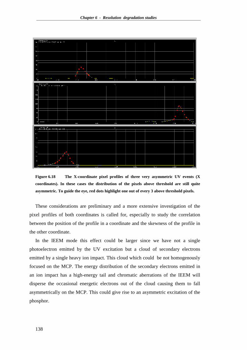
Chapter 6 - Resolution degradation studies
138
Figure 6.18 The X-coordinate pixel profiles of three very asymmetric UV events (X
coordinates). In these cases the distribution of the pixels above threshold are still quite
asymmetric. To guide the eye, red dots highlight one out of every 3 above threshold pixels.
These considerations are preliminary and a more extensive investigation of the
pixel profiles of both coordinates is called for, especially to study the correlation
between the position of the profile in a coordinate and the skewness of the profile in
the other coordinate.
In the IEEM mode this effect could be larger since we have not a single
photoelectron emitted by the UV excitation but a cloud of secondary electrons
emitted by a single heavy ion impact. This cloud which could be not homogenously
focused on the MCP. The energy distribution of the secondary electrons emitted in
an ion impact has a high-energy tail and chromatic aberrations of the IEEM will
disperse the occasional energetic electrons out of the cloud causing them to fall
asymmetrically on the MCP. This could give rise to an asymmetric excitation of the
phosphor.

Chapter 6 - Resolution degradation studies
139
Figure 6.19 The pixel contents of an asymmetric UV event that is skewed to the left. The
difference between the centroid (blue arrow) and the maximum (red arrow) corresponds to a
shift of -1 µm in the reconstructed image.
Until the cause of the asymmetry is understood and accounted for, it is uncertain
if the centroid is the best estimator of the impact position.
Conclusions
Vibrations and optical distortions are not responsible for the still high value of the
spatial resolution and an extensive study of the pixel profile of single events in the
PEEM and IEEM modes is needed, in order to investigate the cause of the
asymmetry and eventually optimize the algorithm that calculates the position of the
light spot. This should improve the resolution of the system.
We will first implement a new feature in STRIDE that will return not only the
centroid of each peak, but also the position of the maximum. With such a feature it
will be possible to distinguish between events with symmetric pixel profiles and
skewed ones.
The resolution studies previously described in this work (correlation peak analysis
in Chapter 5) should be repeated to study how the resolution of a given image is
affected by using different position estimators.
Further studies of resolution as a function of skewness will allow us to assign a
tailored position uncertainty to every event: i.e. the best estimator of the position of a
light spot could be assigned on an event-by-event basis, for example by weighing the

Chapter 6 - Resolution degradation studies
140
centroids and maxima according to where the light spot is detected. In particular
images obtained using only events with symmetric pixel distributions will allow us to
perform a bench-mark measurement of the PEEM/IEEM resolution with which we
will more precisely evaluate other contributions to the degradation of the resolution
of the PEEM/IEEM system such vibrations, membrane scattering and SDRAM
mapping.
Chapter 7 - An IEEM-imaged and time resolved-IBICC experiment with a power MOSFET
141
7 An IEEM-imaged and time resolved
IBICC experiment with a power MOSFET.
7.1 Introduction
In this chapter we describe an Ion Beam Induced Charge Collection (IBICC) type
experiment using a power MOSFET device. This experiment was performed together
with a research group led by Prof. G. Busatto of the University of Cassino (Italy).
The purpose of the experiment was to demonstrate the ability of the IEEM system to
associate precise locations in space and time of the ion impacts with the ion-induced
effects in the MOSFET devices; i.e. to perform time-resolved IBICC experiments.
In this chapter we discuss in some detail the effects of single ion impacts on
power MOSFETs, the need to know the position of the ion impact (hence the
motivation to use the IEEM), the experimental setup and finally a time resolved
IBICC map.
7.1.1 Power MOSFETs
As of 1998, the Cassino group studies the effects of heavy ion irradiation on
power electronic devices. This research has been performed in collaboration both
with INFN and industry (Siemens/Infineon and STMicroelectronics in Catania, Italy)
and carried out at many laboratories (INFN Laboratories of Legnaro and Catania and
UCL, Louvain-la-Neuve, Belgium).
In particular, the longstanding relationship of the Cassino group with
STMicroelectronics has brought the development and systematic experimental study
and testing of two types of radiation tolerant power MOSFETs. The group
significantly contributed to the identification of causes of Single Event Burnout
(SEB) in power MOSFETs, suggested mitigating strategies and tested the new

Chapter 7 - An IEEM-imaged and time resolved-IBICC experiment with a power MOSFET
142
generation of SEB-tollerant devices that belong to two categories: 100V-Nchannel
power MOSFETs and 200V-Nchannel power MOSFETs24.
In what follows we describe the experimental setup and the scientific approach
used to study SEB in these devices.
It is important to recall and keep in mind that MOSFET devices may manifest
Single-Event Gate Rupture (SEGR), another failure mechanism that must be
confronted before a device can be considered radiation tolerant.
7.1.2 MOSFET irradiation experiments: device, setup and
instrumentation
Figure 7.1 is the photograph of typical power MOSFET ready for irradiation. The
die of the device under test, with an area of several square millimeters, is glued on
the rhomboid TO-3 package using a silver electro-thermal conductive paste. The
conductive glue ensures that the metallic package is at the same potential of the drain
electrode (the bottom side metallization of the silicon die), while the gate and source
terminals are wire-bonded to the external rheophores (the two blue circles in Figure
7.1).
Figure 7.1 MOSFET device ready for irradiation. The die is housed a TO-3 package.
24 The work was performed within the GALILEO project (the European GPS project) and
commissioned by the European Space Agency (ESA).

Chapter 7 - An IEEM-imaged and time resolved-IBICC experiment with a power MOSFET
143
Figure 7.2 shows the symmetric structure of the elementary unit cell of the power
MOSFET under test. The lateral size of the characteristic objects of the structure
shown is of the order of tens of microns. The size of the unit cell in the dimension
orthogonal to the page can be accurately thought of as being indefinite. A MOSFET
device is made of hundreds of these unit cells.
The different regions of the elementary unit cell are shown in different colors.
They are, going from bottom to the top: the drain contact (black); the drain region
(light green and yellow); the body or the base region (orange); the source region
(dark green); the oxide region (blue); the surface contacts, body-source and gate
(black).
The active volume of the elementary unit cell, the “channel region”, is located in
the base region just below the oxide; inside it, a region of electronic states can be
formed that conducts electrons.
Figure 7.2 The internal structure of the elementary unit cell of a power MOSFET. The
structure is described in the text.
The device is glued to the TO-3 package on the drain side (the bottom side; see
Figure 7.2) so that, during the ion irradiation experiment, the ions impact the device
from above.

Chapter 7 - An IEEM-imaged and time resolved-IBICC experiment with a power MOSFET
144
As the ion range and the energy deposit along its path in a given material depend
on the ion species and initial energy, we report, as an example, in Figure 7.3 the
Linear Energy Transfer (LET), expressed in eV/Å, as a function of ion depth for a
139 MeV 58Ni ion in bulk silicon with a thin oxide layer. The range is of the order of
tens of microns (23um, in this case) and this implies that most of the ionization
energy loss of the ion occurs inside the impacted unit cell. The figure shown is a
standard SRIM output [63].
Figure 7.3 The LET profile (red) of a 139 MeV 58Ni ion as it penetrates through a thin
silicon oxide layer into bulk silicon.
Before an ion impact occurs the device is OFF (no channel is open): the standard
polarization of the device puts the source electrode at the reference potential
(ground), the control electrode (gate) at zero potential and the drain electrode at a
positive potential. When an ion enters the unit cell, the electron-holes created along
the ion track are subject to the electric field inside the device: the electrons move
towards the positive electrode, the holes move towards the relatively negative ones.
The motion of these charges produces a very short transitory signal on the drain
electrode that can be detected and analyzed by an external acquisition system. The
characteristics of the signal depend on the parameters of the effective circuit.

Chapter 7 - An IEEM-imaged and time resolved-IBICC experiment with a power MOSFET
145
Figure 7.4 The conceptual schematic of the circuit used to test the behaviour of the drain
signal of the irradiated MOSFET. The signal waveforms on the drain electrode are acquired
and memorized by a fast digital oscilloscope and then computer analyzed.
Figure 7.4 shows the schematic of the circuit used to analyze the drain signal
during irradiation. Note that both the drain and gate electrodes are statically polarized
(typically Vgs=0 e Vds>0), but they are capacitively coupled, each with a decoupling
capacitor, to two transmission lines that send waveform signals to the acquisition
system.
The acquisition system of the drain signal waveform on the drain transmission
line is based on a high sampling rate digital oscilloscope (LECROY WavePro
WP7100A, 10 M points/Channel). The waveforms are acquired and memorized and
computer analyzed (post-processed). The impulses on the gate transmission line are
generally uninteresting and are usually ignored. On the other hand the current on the
biasing line of the gate is monitored as it is a direct measure of the ion-induced
damage to the oxide layer.
In summary, during the experiment all the ion-induced drain waveforms are
acquired, as well as the gate bias gate current as a function of time and the ion
fluence.
7.1.3 MOSFET experiments: typical results
When exposed to heavy ions, MOSFET devices show a threshold behaviour: the
activation of a single event damage effect (e.g. SEB) may occur only when certain
minimal electrical conditions are imposed.

Chapter 7 - An IEEM-imaged and time resolved-IBICC experiment with a power MOSFET
146
As an example Figure 7.5 (a) shows some typical ion-induced drain current-pulses
of a 200 V MOSFET device for a given ion species and energy (in this case 139
MeV 58Ni ions): the pulse duration is of the order of tens of nanoseconds and the
wave-forms vary in amplitude. For certain electrical conditions (e.g. a certain static
drain voltage) one can measure the average integrated charge of the ion-induced
drain current-waveforms. Figure 7.5(b) shows the average integrated charge of the
drain-waveforms at different static drain voltages for three different types of
MOSFET devices. In this experiment the drain-voltage on the devices was increased
and the increasing average charge of each device was recorded until it was destroyed
by a SEB event (red points in the figure). The particular dependence of the charge
with drain-voltage depends on the device type; it also depends on the ion species and
energy. For the experimental data shown the gate voltage was kept at the reference
value (Vgs = 0V).
As can be seen in Figure 7.5(b), for a SEB to occur the drain-voltage must be high
enough: for drain-voltages above the threshold value, the probability of a SEB is
significant and increases with voltage. For drain-voltages comparable to the
breakdown voltage, the probability of destruction approaches certainty; i.e. a SEB
will almost certainly occur at the very first ion impact. For voltages below the
threshold values the probability of a SEB is negligible and the device can survive the
impacts of many ions.
Figure 7.6 shows the typical experimental distribution of the integrated charge of
the drain-pulse (dark-blue) for a certain drain voltage. The distribution is composed
of two types of event: in this case, there is a large population peaked at 5 pC and a
smaller second population with a higher charge (peak at ∼7.5 pC). The relative size
and peak charge of the second population increase with drain-voltage, while the peak
charge of the first population does not significantly change. The bimodal form of the
experimental distribution can be modelled using two Γ-probability distribution
functions (pdf): the light-blue histogram in Figure 7.6 is obtained by generating
random numbers from the two Γ-pdfs in an opportune proportion (6 to 1).
Studies performed by the Cassino group have shown, with the help of finite-
element simulations, that the second larger-charge population of drain-pulses is due
to the transitory activation of a parasitic N-P-N structure inside the MOSFET with a
probability of activation that increases with the drain voltage. These studies allowed

Chapter 7 - An IEEM-imaged and time resolved-IBICC experiment with a power MOSFET
147
the group to propose mitigation strategies that solved the SEB problem by raising the
activation threshold of the parasitic transistor in the MOSFET devices.
a)
b)
Figure 7.5 a) several overlaid drain-electrode impulses of a 200 V MOSFET impacted by
139 MeV 58Ni ions. Conditions: Vds = 40 V, Vgs=0V. b) The dependence of the average
integrated charge of three device types under test for different drain voltages (Vds) with
Vgs=0. The red points indicate when the corresponding device was destroyed by SEB.

Chapter 7 - An IEEM-imaged and time resolved-IBICC experiment with a power MOSFET
148
Figure 7.6 In dark blue the experimental distribution of the integrated charge of the
current pulses on the drain electrode due to ion impacts for a given drain-voltage. In light
blue a numerical distribution composed of two ΓΓΓΓ-like populations.
7.1.4 Motivation to obtain ion-impact position information
It must be stressed, at this point, that the SEB problem of power MOSFETs has
been extensively discussed over the years and solved. On the contrary, the
vulnerability to Single Event Gate Rupture (SEGR) shows several aspects that still
need to be further studied.
The rupture of the gate oxide can occur even at reduced drain voltages and with
zero or very small gate voltages (few volts). In addition the gate rupture is a delayed
phenomenon; it may occur hours after a single ion impact and it is usually
accompanied by instabilities (telegraph noise) in the leakage current through the
oxide.
To better understand this phenomenon two- and three-dimensional finite-element
simulations have been performed over the years to study the effect of a heavy ion
impacts in a elementary cell of a MOSFET.
Figure 7.7 shows the mix-mode circuit of the device; i.e. part is finite-element (the
elementary cell of the MOSFET) while part is with discrete components. The
discrete part accounts for the parasitic effects of the package and the connections of
the device to the external world. Three ion trajectories are considered (shown in the
figure as dashed lines): (a) at the centre of elementary cell (neck region); (b) at the

Chapter 7 - An IEEM-imaged and time resolved-IBICC experiment with a power MOSFET
149
drain-side edge of the conductive channel; (c) at the source-side of the conductive
channel.
Figure 7.7 Mixed-mode circuit used for the finite-element analysis. The dashed lines
represent three trajectories of incident ions. The discrete part accounts for parasitic effects
due to the package and real-world connections.
The goal of simulations is to study the electrical connections (static and dynamic)
and the characteristics of the incident ion (species, energy, position of impact) that
cause significant stress to the oxide layer. To model the effect of a 139 MeV 58Ni ion
impact, a charge of a few pC is deposited along a trajectory with a longitudinal
dependence given by the LET-vs-depth distribution shown in Figure 7.3.
a)
b)
Figure 7.8 2D distribution of the electric field inside the device at the instant of maximum
electric stress, a few picoseconds after an ion impact. a): ion trajectory (a) of Figure 7.7. b):
ion trajectory (b).

Chapter 7 - An IEEM-imaged and time resolved-IBICC experiment with a power MOSFET
150
Figure 7.8(a) and 9.8(b) show the 2D distribution of the electric field inside the
device at the instant of maximum electric stress, a few picoseconds after the
modelled ion impact, along the trajectories (a) and (b) shown in Figure 7.7 [64]. As
one can see from the figure, the simulated electric field reaches 106 V/cm inside the
oxide layer, in correspondence to the impact point of the ion, above the neck region
(a), or above the channel region (b). Such values of electric field, close to the
dielectric strength25 of the SiO2 may favour the formation of a permanent damage to
the structure of the oxide This is at present the best theory to explain the damage of
the oxide layer during ion irradiation. Unfortunately the finite-element simulations
are limited as they do not implement the local ion-induced breakdown mechanism of
an oxide layer (a stochastic phenomenon). For this reason the formulation of a
definitive model of the oxide damage and eventually the SEGR breakdown is not yet
reached.
Figure 7.9 shows the time dependence of the maximum electric field for the three
ion impact points shown in Figure 7.7. The effect of the impact position is very
significant: the peak of the E-field is higher when the ion impacts the centre of the
elementary cell (point a, the neck region).
Figure 7.9 The time dependence of the maximum electric field for the three ion impact
positions shown in Figure 7.7.
The simulations have only been partially successful: they gave important results,
like showing that SEGR has a strong dependence on the impact position of the ion,
25 The maximum electric field an insulating material can withstand without breaking down.

Chapter 7 - An IEEM-imaged and time resolved-IBICC experiment with a power MOSFET
151
but they also proved to be limited by the great difficulty to model the oxide layer and
the phenomena that take place in it. The oxide layer may manifest percolative
damage (that is, a constant and significant leakage current), or multi-hop quantum
tunnelling effects that show a threshold behaviour and that degenerate with time. In
addition, the holes in the oxide have a very small mobility (of the order of a
micron/year) and they may accumulate, especially at the interface with the
underlying semiconductor, and alter its conductivity.
The phenomenology of the damage to the oxide layer is complex and
experimentally varied. Figure 7.10(a) shows the behaviour of the gate leakage
current of a non-irradiated device under static polarization while Figure 7.10(b)
shows the post-irradiation time dependence of the gate leakage of a device just after
it has been exposed to 30 ion impacts. The leakage current of the irradiated device is
not only higher and noisier, but it worsens over a time scale of an hour with peculiar
characteristics:
• the leakage current does not increase continuously but gets worse in discrete
jumps;
• the amount of the current jump and the instant it occurs are not predictable
(stochastic);
• the noise of the leakage current is telegraphic (stochastic spikes);
• the peak-to-peak noise amplitude increases with the leakage current (the noise
worsens for each new discrete jump);
• the process is irreversible (no annealing) and the oxide is permanently damaged.
To further complicate the phenomenon, it sometimes happens that the post-
irradiation time dependence of the gate leakage current is almost linear (Figure 7.11),
until a sudden catastrophic failure of the gate occurs: the leakage current goes out of
control and the gate, for all practical purposes, is short-circuited.

Chapter 7 - An IEEM-imaged and time resolved-IBICC experiment with a power MOSFET
152
a)
b)
Figure 7.10 a) The time dependence of the gate leakage current of a non-irradiated
(fresh) device. b) The post-irradiation time dependence of the gate leakage current just after
exposure to 30 ions.
Figure 7.11 The post-irradiation gate leakage of an irradiated device that shows an
unpredictable catastrophic failure of the gate oxide (the current is out of control).
This experimental behaviour leads to the theory of latent gate oxide damages
[65]. The oxide layer stressed by the high electric field is not destructively damaged:
only a very localized region (few Å) of the oxide is weakened. This weakened region
gradually degenerates until high values of leakage or until breakdown. In this
hypothesis, the stochastic behaviour can be due to:
• the position of the ion impact respect to the elementary cell;
• the impact of a new ion near a region weakened by a previous ion impact.

Chapter 7 - An IEEM-imaged and time resolved-IBICC experiment with a power MOSFET
153
In this confusing setting, it is clearly very useful to have an experimental system
to recognize the impact point of a heavy ion in an elementary cell with a precision of
at least a few microns.
Energetic heavy ion microbeams are very useful, but are not easy to come by.
The availability of the IEEM has now opened up new interesting opportunities.
7.1.5 The IEEM experiment
The first step when using the IEEM of the SIRAD facility is to adapt the device
under study (DUT) to the mechanical and electrical constraints of the IEEM system.
However the volume of the experimental vacuum chamber is enough to
accommodate large devices and electronic boards.
The most important constraint of the IEEM system is the need to minimize the
distance of the DUT from the ultra-thin Au-Si3N4 membrane. In practice this means
that ideally the DUT should be the closest object to the plane of the membrane; i.e.
no feature of the device board with any ancillary electronics should stick out more
than the surface of the DUT. In many cases this is not possible, for example: the wire
bonds that connect the DUT to the board cannot be removed or arbitrarily shortened.
Therefore the distance between the membrane and the DUT has to be adjusted to
accommodate the bonds. In this experiment the distance of the MOSFET from the
ultra-thin Au-Si3N4 membrane was comfortably set at 0.8 mm.
Figure 7.12 shows the MOSFET with its TO-3 package mounted on a board we
purposely designed for the IEEM experiment. Two gate micro-wires from the top
rheophore are bonded to a small rectangular pad visible at the top of the MOSFET;
four source wires from the bottom rheophore are bonded to the centre of the
MOSFET (the backside drain connection is made inside the TO-3 package). The
figure also shows the PIN diode we use to perform beam setup.

Chapter 7 - An IEEM-imaged and time resolved-IBICC experiment with a power MOSFET
154
Figure 7.12 A photograph of the MOSFET with its TO-3 package mounted the test board.
A PIN diode (bottom right) with reference copper strips on top is used for beam setup and
for determining reference positions.
The beam setup procedure consists in moving the PIN diode into the field of view
of the IEEM. The beam transport is verified and adjusted: ion flux is set and the
beam quality (mono-chromaticity) is checked. We recall that the diode has small
copper strips placed on top that partially screen the sensitive area (Figure 7.12); a
IEEM sensitivity map of diode is made (see Chapter 5) and the extremities of the
copper strips are used as reference points that are needed to identify points of interest
on the MOSFET.
We performed the experiment using 223 MeV 79Br ions. To image the copper
strips on the PIN diode, we use a high flux of ∼1000 ions/s in the field of view of the
IEEM. Once the copper reference points were reconstructed, the ion flux was
lowered to ∼20 ions/s in the IEEM field of view. The beam was then interrupted
while the MOSFET was moved into the field of view.

Chapter 7 - An IEEM-imaged and time resolved-IBICC experiment with a power MOSFET
155
The MOSFET drain-source voltage Vds was initially set to 10 V, a cautionary
value low enough to avoid large destructive effects.
Current transients on the drain of the MOSFET, above an adjustable threshold,
were used to generate LVDS signals that were used by STRIDE to tag the ion impact
signals. Figure 7.13 shows a typical wave-form. The threshold was set at Vth = 6 mV
over 50 Ω (corresponding to a peak current of 120 µA).
At this voltage only the drain signals of the areas of the MOSFET where the
electrical field is the highest are above threshold and can tag STRIDE events.
Therefore ions that strike the gate distribution line and the polysilicon fingers shown
in Figure 7.14(a) cannot produce drain-transients above threshold as expected by the
model discussed in 9.1.5 (see Figure 7.7 and Figure 7.8). The STRIDE events tagged
by above threshold drain signals quickly built up a sensitivity map in real time,
allowing us to immediately recognize the sensitive areas: the metal lines of the
source contacts (Figure 7.14(b).
Figure 7.15(a) shows the map of tagged IEEM ion impacts: the gate distribution
line and the polysilicon fingers are evident. Events were also analyzed off line
searching for time coincidences between the drain recorded signal set and the
STRIDE event one in a 106 ms window (the readout time of STRIDE) . Figure
7.15(b) shows the subset of the tagged IEEM events of 9.15(a) time correlated with
the drain signals.
0 50 100 150 200
0
50
100
150
Time [ns]
Cur
rent
[µA
]
Figure 7.13 A drain-waveform with Vds = 10 V due to an 223 MeV 79Br ion. The signal is
above the tagging threshold of Vth = 6 mV and was used to tag a STRIDE event.

Chapter 7 - An IEEM-imaged and time resolved-IBICC experiment with a power MOSFET
156
a)
b)
Figure 7.14 a) Layout of the 200 V power MOSFET used in this experiment.
b) Microphotograph of the metalized surface of the device. In the circle the detail of the
surface metallization at the edge of the gate distribution line (the thick vertical line). The
horizontal thin white lines correspond to the polysilicon fingers.
a) b)
Figure 7.15 a) On line image with the tagged STRIDE events (2333 events). The gate
distribution line and the polysilicon fingers are evident. b) The events of (a) that are time-
correlated with an above threshold drain signal (off-line analysis).
The numbers of recorded drain signals, of tagged STRIDE events and of their
coincidences are summarized in the following table:
Drain signals over threshold Tagged STRIDE events Coincidences 3691 2333 2235
The fraction of the tagged STRIDE events that are in coincidence with a LeCroy
drain-waveform is 95.8%; the fraction of LeCroy drain-waveforms that are found to
be in coincidence with a STRIDE event is 61%. Of the tagged STRIDE events, a
small number of events (123) are not found among the events saved by the digital

Chapter 7 - An IEEM-imaged and time resolved-IBICC experiment with a power MOSFET
157
oscilloscope. A fraction of the drain-current transients above threshold (that tag the
STRIDE events) are not recorded by the LeCroy oscilloscope. This occurs when the
buffer memory of the LeCroy is full and the buffered wave-forms are copied to the
hard disk drive; during the writing time the oscilloscope does not save new
waveforms, but the trigger continues to work and STRIDE continues to acquire
tagged events.
Once the interesting region of the MOSFET was recognized and the tagging
system verified, the working voltage of the MOSFET was raised from the 10 V
cautionary value to a more realistic and hence interesting value (70 V). The drain-
waveforms were now correspondingly more robust: Figure 7.16 shows waveforms
recorded by the LeCroy digital oscilloscope when exposed to the 223 MeV 79Br ions
(the figure also reports the integrated charge). In these working conditions almost all
the STRIDE events are tagged and an online sensitivity mapping does not show any
features as all the drain signals are now over threshold.
0 20 40 60 80 100
0
0.2
0.4
0.6
0.8
1
Time [ns]
Cur
rent
[mA
]
charge<6pC6pC<charge<7pC7pC<charge<8pCcharge=16pC
Figure 7.16 Four 223 MeV 79Br ion induced drain-waveforms recorded during the
experiment. All four transients generated a tag signal.
The off-line time-correlation analysis of drain signals and STRIDE events has
been performed as a function of the integrated charge of the drain-waveforms. The
evolution of the STRIDE image is reported in Figure 7.17 from (a) to (c) for different
charge intervals and Vds=70 V. The distribution of events with integrated charge <
6pC of Figure 7.17(a) shows the gate distribution line already observed in Figure
7.15. However the line is heavily shrunk. Figure 7.17(b) shows that the events with
integrated charge between 6 pC and 7 pC come to populate two bands parallel to that

Chapter 7 - An IEEM-imaged and time resolved-IBICC experiment with a power MOSFET
158
observed in Figure 7.17(a). These three bands almost recover the area of the gate
distribution line of Figure 7.15, but they are clearly separated among them indicating
a threefold structure of the electrical field below the gate. All this structure becomes
insensitive when only high charge events are selected (Figure 7.17(c)). The gate-
contact polysilicon lines are still discernable as areas of small drain signals.
Data must be further analyzed and compared with careful simulations of the
MOSFET. By the way these first results demonstrate the capability of the IEEM
system to provide in-deep information of the structure of state-of-the-art electronic
devices.
a) b)
c)
Figure 7.17 Reconstructed positions of ion impacts; for different charge pulses induced
in the drain terminal: small charges (a) ,medium (b) and large charges (c). Arbitrary units
on the axes.

Chapter 7 - An IEEM-imaged and time resolved-IBICC experiment with a power MOSFET
159
Figure 7.18 Reconstructed positions of ion impacts; the different colours accounts for
different charge pulses induced in the drain terminal.
This preliminary experiment demonstrates the ability of the IEEM system to study
ion-induced charge collection effects.

Chapter 7 - An IEEM-imaged and time resolved-IBICC experiment with a power MOSFET
160

Chapter 8 - SOI Imager Shift Register SEU map
161
8 SOI Imager Shift Register SEU map
8.1 Introduction
The SOI Imager is a prototype monolithic pixel detector for charged particle
detection and imaging applications, designed and fabricated using a commercially,
deep-submicron Silicon-On-Insulator (SOI) process, in a 0.20 µm technology [66].
In this process, a buried oxide layer (BOX) is employed to insulate a thin layer of
integrated full CMOS electronics from a high-resistivity substrate. The substrate
allows pixel implanting and reverse biasing and is contacted from the electronics
layer through vias etched in the buried oxide. The sensitivity to SEUs of the whole
chip is high, because at this stage of the project no caution by design was adopted to
limit it. In this way the chip is a good test bench to measure the performances of the
IEEM in mapping the Single Event Upset (SEU) sensitivity.
8.2 SOI Imager Shift Register
The IEEM system was recently used to map the sensitivity to SEU of the Shift
Register (SR) of the SOI Imager chip (the schematic in Figure 8.1; a
microphotograph in Figure 8.2).
In this chip, the sensitive area is a 3.5×3.5 mm2 array of 256×256 equally spaced
pixels (13.75 µm pitch) driven in a standard serial readout scheme. To increase the
readout speed, the pixel matrix is divided into 4 parallel arrays of 64 columns each
connected to 4 identical parallel output analog stages, external to the pixel matrix.
Besides the analog stages, in the periphery of the pixel matrix the electronics for row
and column selection is also implemented. Five SR are used to access one by one the

Chapter 8 - SOI Imager Shift Register SEU map
162
256×256 pixels in which the sensitive area is partitioned: one SR is for the rows
addressing and four SR (one for each sector) for the columns addressing; they consist
of a chain of cells (256 for the row SR and 64 for the column SR), each connected to
one row (column) of the pixel array.
Figure 8.1 Layout of the SOI-Imager chip. The position of the row and column SR is
marked by the arrows.
During the readout operation, all the cells of the SR are in the same inactive logic
state, except one, which activates the relative row (column). At every clock cycle, the
active column-SR cell deactivates, inducing the activation of the subsequent one. The
process continues until the deactivation of the last cell that re-initializes the
activation succession from the first column in the column-SR. At the same time a
pulse signal is sent at the clock gate of the row-SR that selects a new row. In this way
the whole sensitive area of the sensor is read in a line-by-line fashion.

Chapter 8 - SOI Imager Shift Register SEU map
163
Figure 8.2 Microphotograph of the upper portion of the SR of the SOI-Imager chip.
The cells of the SR are hidden below the two thick vertical metallisation lines at the centre.
On the right the pixel array of the Imager is visible. During the experiments the pixels were
shielded and not exposed to the ion beam.
8.3 SEU global cross section measurement
With respect to SEU, SOI devices were traditionally considered more radiation
hardened than the ones manufactured in standard bulk CMOS technology. In fact the
charge collection volume was assumed to be much smaller, as only carriers generated
in the top thin silicon layer were believed to contribute to the charge induction build-
up. In the past, SEU tests seemed to support this assumption [2]. Most recently, new
SEU tests on SOI static random access memories (with BOX thicknesses less than
200 nm) showed unexpectedly high SEU cross-sections [3]. This can be correlated to
Ion Beam Induced Charge Collection (IBICC) measurements which revealed that the
amount of induced charge is much larger than just the charge deposited onto the top
silicon layer above the BOX [4][5]. There is a clear indication that charge induction,

Chapter 8 - SOI Imager Shift Register SEU map
164
at least for some technologies, occurs not only when the carriers move in the top
silicon layer but also when they move below the BOX. These considerations show
that a detailed study of the behavior of SOI pixels is required in order to measure
their effective SEU sensitivity, assess their application limits in radiation
environments and to define a possible R&D path towards radiation tolerant sensors.
The SEU cross section has been measured for the SOI-Imager chip at the SIRAD
broad-beam irradiation facility (sez. 4.5). In our prototype chip, the row-SR is
provided with pad connections to control it independently from the rest of the chip
and to monitor the output activity. A microcontroller is used to drive the SR and read
its output with a 125 kHz clock frequency. The pattern loaded in the SR is a
sequence of 255 cells at “0” and only one cell at “1”, the only one allowed by design
(an arbitrary sequence cannot be written). Once completely loaded, the SR was
exposed to heavy ion irradiation and its content read-out. Any logic value which
differed from the loaded one was assumed to be caused by a SEU that occurred in the
cells. Irradiations were performed using three different ions in the order of
decreasing LET (79Br, 35Cl, then 19F; see Table 10.1). For each ion beam, two
irradiations were made: one with substrate bias conditions Vbias = 0 V (i.e. no bias
applied to the detector) and one with Vbias = 7 V (~20 µm of depletion depth in the
substrate). For all ion beams, the maximum of ionization (the Bragg peak) occurs in
the high resistivity bulk, below the BOX.
Table 8.1 Energy, range in Silicon and surface LET values for the ion species used in the
global irradiation experiment.
In this experiment no “1” → “0” were detected, while ∼66% of the times the SR
was readout a “0” → “1” transition was detected. As only one cell of the SR is in the
logic state “1”, the transitions from the logic state “1” to the logic state “0” are rare
compared to the “0” → “1” transitions. Due to lack of statistics we cannot state that
Ion species
Energy (MeV)
Range in Si (µm)
LET0 in Si (MeV·cm2/mg)
19F 118 93 3.67 35Cl 170 49 12.5 79Br 240 32 38.6

Chapter 8 - SOI Imager Shift Register SEU map
165
the SEU probability might depend on the logic state of the irradiated cell. Fear for
possible total dose effects has drastically limited the collected statistics.
Figure 8.3 SEU cross section measurements of the SOI-Imager with bias (top) and with no
bias (bottom) applied to the detector. Circles are experimental data, the continuous line is
the Weibull fit [6].
The measured SEU cross sections are shown in Figure 8.3 for the two bias
conditions previously described. No significant differences can be observed in the
LET threshold (LETthr ~ 4 MeV cm2/mg), nor in the saturated cross section (σsat ~
10-6 cm2). However, the same chip was used for all the irradiations and the total dose
damage, up to 140 kRad at the end of the irradiation, cannot be neglected. At the end
of the irradiation, pixels exposed to the ion beam show a significantly higher noise
level than the non-exposed pixels, due to an increase in the leakage current. We also
noticed that the device supply current also increased, and we couldn’t apply a Vbias >

Chapter 8 - SOI Imager Shift Register SEU map
166
1 V, confirming that total dose effects were turned on (high leakage current in the
transistors).
In evaluating the above results, it must be recalled that the chip was designed with
no radiation tolerance in mind at all, so it does not sport any specific hardening
toward both total dose and single event upset. On the contrary, this feature was
crucial to get unambiguous evidence that the SOI technology is very sensitive to
single high charge depositions below a 200 nm BOX.
8.4 SEU micro-mapping
The SIRAD IEEM system was used to map the sensitivity to Single Event Upset
(SEU) of the Shift Register (SR) of the SOI-Imager detector. The row shift register
(below the vertical metallization lines of Figure 8.2) was positioned in the field of
view of the IEEM using the standard copper-profile reference point technique
described in Chapter 7. A microcontroller was used to drive and readout the SR. In
this experiment the chip was placed at a distance of ∼450 µm from the ultra-thin Au-
Si3N4 membrane, and was irradiated with a 241 MeV 79Br ion beam. The ion impact
rate used in the experiment was 1 kHz.
In the absence of upsets, we expect to find the SR output in the inactive state (“0”)
during the first 255 clock pulses following the initialization procedure and to find it
in an active state (“1”) only during the next clock pulse, which closes the readout
process and re-initializes the device. When ever an upset is found in the readout
sequence, the microcontroller enables the flag signal delivered to STRIDE for 10 ms;
during this period, all the events detected by the DAQ are flagged. During offline
analysis, the flag signal is used to select all the ions previously recorded by the IEEM
system in a time-interval of 2 ms: the readout time of the whole register. The impact
positions of all these selected ions feed a histogram used to plot the SEU map (Figure
8.4).
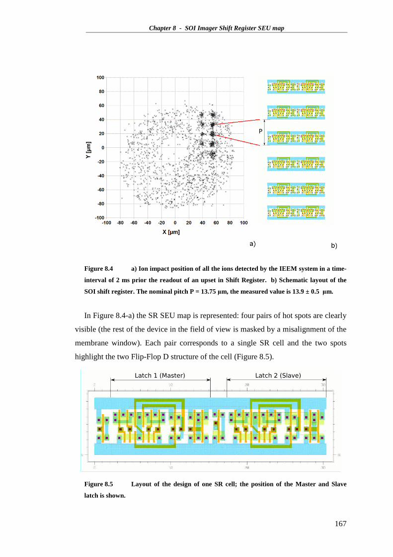
Chapter 8 - SOI Imager Shift Register SEU map
167
Figure 8.4 a) Ion impact position of all the ions detected by the IEEM system in a time-
interval of 2 ms prior the readout of an upset in Shift Register. b) Schematic layout of the
SOI shift register. The nominal pitch P = 13.75 µm, the measured value is 13.9 ± 0.5 µm.
In Figure 8.4-a) the SR SEU map is represented: four pairs of hot spots are clearly
visible (the rest of the device in the field of view is masked by a misalignment of the
membrane window). Each pair corresponds to a single SR cell and the two spots
highlight the two Flip-Flop D structure of the cell (Figure 8.5).
Figure 8.5 Layout of the design of one SR cell; the position of the Master and Slave
latch is shown.

Chapter 8 - SOI Imager Shift Register SEU map
168
The different number of upsets in the two columns is due to the fact that, although
the two Flip-Flop are identical, the logical states are not: the Slave Flip-Flop is
always complimentary to the Master Flip-Flop.
The distance among the centroids of the four pairs amounts to 13.9 ± 0.5 µm and
15.1 ± 0.5 µm, in the Y and X axis of Figure 8 respectively, to be compared to the
13.75 µm and 15.2 µm design values (Figure 8.4-b). The spots show a Gaussian
distribution (σ ∼ 2.5 µm). The present resolution of the IEEM does not allow us to
untangle the most sensitive nodes inside the cell (we cannot say what transistor is
responsible for an upset), but it is sufficient to distinguish the two Flip-Flops and
characterize their relative sensitivity: the Master Flip-Flop is 2.6±0.1 times more
sensitive than the Slave.

Conclusions
169
Conclusions
The SIRAD axial IEEM is now a mature system and we have entered a new phase. The
experience with the SDRAM diagnostic system was very important; having to solve many
and diverse problems (from mechanical to electronic) allowed us then to be able to quickly
change focus and gears and finally perform original and interesting experiments, such as the
one with the power MOSFET. A new vigorous collaboration with the Cassino group has
begun and new IEEM experiments are planned. The issue of the effective resolution of the
IEEM needs more work but its was very important for us to prove, to avoid chasing a red
herring, that the SDRAM needs to be completely mapped. However at this point a far more
interesting option is to change the type of pixelated device to measure the resolution. We
have already begun a collaboration with a group with the Department of Information
Engineering (DEI) of the University of Padova that studies the effects of single ion impacts
in FLASH devices. The resolution degradation studies were successful as they point the way
for effective upgrades, for example the STRIDE firmware must be changed to allow the
possibility to improve the position estimator off-line. We are confident we can measure and
somewhat improve the resolution with minor changes, but we also strongly feel that the best
strategy is to make the IEEM system more flexible, user friendly and hence an attractive tool
to users.
One way to make the IEEM system much more flexible is already under design: the ultra-
thin Au-Si3N4 membrane will be used to partition space into two volumes: a high vacuum
portion with the IEEM, and a low vacuum volume with the device under test. A high vacuum
is needed to put high voltage on the MCP inside the IEEM. At present any out-gasing of the
device under test makes the pump-down time very long (3-5 hours, if not more with some
types of DUTs with complex boards). In the new partitioning the MCP would always be in
high-vacuum and can be turned on at any time, while the DUT chamber would require short
pump-down times: the DUT would be moved close to the membrane so that the vacuum
required before irradiation could be achieved in minutes. At higher energy accelerators the
DUT irradiation could be done in air (the membrane can withstand air-pressure). The
Conclusions
170
membrane/DUT distance does affect the effective resolution but our work has shown that
interesting values can be achieved with millimetric distances (∼1-2mm) that could easily
accommodate almost any type of device, posing almost no mechanical and electrical
constraints to the user.
We have crossed many hurdles, learned a great deal and with persistence have
successfully reared the IEEM at SIRAD. In retrospect we remain confident in believing that
the IEEM system will now make the already successful facility even more attractive: SIRAD
now offers both global and micrometric possibilities for a wide selection of heavy ions. The
facility suffers much from too little beam time, but we hope that the success of the latest
experiments will help make matters improve.
An IEEM system is non-invasive, flexible and only slightly worse than that of the
very best energetic heavy ion microbeams. The traditional microbeam approach is
arguably the preferred one, as one can decide where the next ion is going to strike,
but it certainly needs far greater development as it is challenging to focus a wide
variety of energetic heavy ion beams down to micron size. On the other hand an
IEEM can be easily installed by a small group of people on a pre-existing and
successful beam-line at any high energy heavy ion accelerator (cyclotron, post-
accelerators,…) that can deliver ions with greater range and are more suitable to test
the latest microelectronic devices.

Bibliography
171
Bibliography
[1] S. M. Sze, Physics of Semiconductor Devices (Wiley, New York, 1981).
[2] E. L. Petersen, “Single Event Analysis and Prediction”, 1997 IEEE NSREC Short
Course, Snowmass, CO.
[3] T. Pierce, M. Blann, “Stopping Powers and Ranges of 5-90-MeV S32, Cl35, Br79,
and I127 Ions in H2, He, N2, Ar, and Kr: A Semiempirical Stopping Power Theory
for Heavy Ions in Gases and Solids” Phys. Rev., 173 (1968) 390.
[4] C. M. Hsieh, P. C. Murley, and R. R. O’Brien, “A field-funneling effect on the
collection of alpha-particle generated carriers in silicon devices,” IEEE Electron
Device Lett., vol. 2, no 4, pp 103-105, 1981.
[5] P. E. Dodd, “Device simulation of charge collection and single-event upset,” IEEE
Trans. Nucl. Sci., vol. 43, no. 2, pp. 561-575, 1996.
[6] H. Schöne, D. S. Walsh, F. W. Sexton, B. L. Doyle, P. E. Dodd, J. F. Aurand, R. S.
Flores, N. Wing, “Time-resolved ion beam induced charge collection (TRIBICC)
in microelectronics,” IEEE Trans. Nucl. Sci., vol. 45, no. 6, pp. 2544-2549, 1998.
[7] J. R. Srour, C. J. Marshall, P. W. Marshall, “Review of displacement damage
effects in silicon devices,” IEEE Trans. Nucl. Sci., vol. 50, no. 3, 2003.
[8] D. Binder, E. C. Smith, and A. B. Holman, “Satellite anomalies from galactic
cosmic rays,” IEEE Trans. Nucl. Sci., vol. 22, pp. 2675–2680, Dec. 1975.
[9] T. C. May and M. H. Woods, “Alpha-particle-induced soft errors in dynamic
memories,” IEEE Trans. Electron. Devices, vol. 26, pp. 2–9, Feb. 1979.
[10] J. C. Pickel and J. T. Blandford, Jr., “Cosmic ray induced errors in MOS memory
cells,” IEEE Trans. Nucl. Sci., vol. 25, pp. 1166–1171, Dec. 1978.
[11] R. C. Wyatt, P. J. McNulty, P. Toumbas, P. L. Rothwell, and R. C. Filz, “Soft
errors induced by energetic protons,” IEEE Trans. Nucl. Sci., vol. 26, pp. 4905–
4910, Dec. 1979.

Bibliography
172
[12] C. S. Guenzer, E. A. Wolicki, and R. G. Allas, “Single event upset of dynamic
RAM’s by neutrons and protons,” IEEE Trans. Nucl. Sci., vol. 26, pp. 5048–5053,
Dec. 1979.
[13] J. L. Andrews, J. E. Schroeder, B. L. Gingerich, W. A. Kolasinski, R. Koga, and S.
E. Diehl, “Single event error immune CMOS RAM,” IEEE Trans. Nucl. Sci., vol.
29, pp. 2040–2043, Dec. 1982.
[14] A. E. Giddings, F.W. Hewlett, R. K. Treece, D. K. Nichols, L. S. Smith, and J. A.
Zoutendyk, “Single event upset immune integrated circuits for Project Galileo,”
IEEE Trans. Nucl. Sci., vol. 32, pp. 4159–4163, Dec. 1985.
[15] F. Faccio, K. Kloukinas, A. Marchioro, T. Calin, J. Cosculluela, M. Nicolaidis, and
R. Velazco, “Single event effects in static and dynamic registers in an a 0.25 µm
CMOS technology,” IEEE Trans. Nucl. Sci., vol. 46, pp. 1434–1439, Dec. 1999.
[16] M. P. Baze, S. P. Buchner, and D. McMorrow, “A digital CMOS design technique
for SEU hardening,” IEEE Trans. Nucl. Sci., vol. 47, pp. 2603–2608, Dec. 2000.
[17] J. Barak J. Levinson, M. Victoria, and W. Hajdas, “Direct processes in the energy
deposition of protons in silicon,” IEEE Trans. Nucl. Sci., vol. 43, no. 6, pp. 2820-
2826, 1996.
[18] S. Duzelier, R. Ecoffet, D. Falguère, T. Nuns, L. Guibert, W. Hajdas, M. C. Calvet,
“Low energy proton induced SEE in memories,” IEEE Trans. Nucl. Sci., vol. 44,
no. 6, pp. 2306-2310, 1997.
[19] T. C. May and M. H. Woods, “A new physical mechanism for soft errors in
dynamic memories,” Proc. IEEE Int. Reliability Phys. Symp., pp. 33-40, 1978.
[20] L. W. Massengill, “Cosmic and terrestrial single-event radiation effects in dynamic
random access memories,” IEEE Trans. Nucl. Sci., vol. 43, no. 2, pp. 576-593,
1996.
[21] T. V. Rajeevakumar, N. C. Liu, W. H. Henkels, W. Hwang, and R. Franch, “A new
failure mode of radiation-induced soft errors in dynamic memories,” IEEE
Electron Dev. Lett., vol. 9, no. 12, pp. 644-646, 1988.
[22] C. L. Axness, H. T. Weaver, J. S. Fu, R. Koga, and W. A. Kolasinski,
“Mechanisms leading to single event upset,” IEEE Trans. Nucl. Sci., vol. 33, no. 6,
pp. 1577-1580, 1986.
[23] H. T. Weaver, C. L. Axness, J. S. Fu, J. S. Binkley, and J. Mansfield, “RAM cell
recovery mechanisms following high-energy ion strikes,” IEEE Electron Device
Lett., vol. 8, no. 1, pp. 7-9, 1987.
[24] J. R. Schwank, P. E. Dodd, M. R. Shaneyfelt, G.Vizkelethy, B. L. Draper, T. A.
Hill, D. S. Walsh, G. L. Hash, B. L. Doyle, and F. D. McDaniel, “Charge

Bibliography
173
collection in SOI capacitors and circuits and its effect on SEU hardness,” IEEE
Trans. Nucl. Sci., vol. 49, pp. 2937–2947, 2002.
[25] W. J. Shaptor, J. P. Meyers, J. B. Langworthy, E. L. Peterson, “Two parameter
Bendel model calculations for predicting proton induced upset”, IEEE Trans. Nucl.
Sci., vol. 37, pp. 1966, 1990.
[26] G. R. Hopkinson, C. J. Dale, and P. W. Marshall, “Proton effects in charge-
coupled devices,” IEEE Trans.Nucl. Sci., vol. 43, no. 2, pp. 614-627, 1996.
[27] J. L. Titus, C. F. Wheatley, K. M. Van Tyne, J. F. Krieg, D. I. Burton, and A. B.
Campbell, “Effect of ion energy upon dielectric breakdown of the capacitor
response in vertical power MOSFETs,” IEEE Trans. Nucl. Sci., vol. 45, no. 6, pp.
2492-2499, 1998.
[28] J. L. Titus and C. F. Wheatley, “Experimental studies of single-event gate rupture
and burnout in vertical power MOSFETs,” IEEE Trans. Nucl. Sci., vol. 43, no. 2,
pp. 533-545, 1996.
[29] A. W. Waskiewicz, J. W. Groninger, V. H. Strahan, and D. M. Long, “Burnout of
power MOS transistors with heavy ions of Californium-252,” IEEE Trans. Nucl.
Sci., vol. 33, no. 6, pp. 1710-1713, 1986.
[30] J. C. Pickel and T. J. Blandford Jr., “Cosmic ray induced errors in MOS memory
cells”, IEEE Trans. Nucl. Sci., vol. NS−25, pp. 1166, 1978.
[31] E. L. Petersen, J. B. Langworthy and S. E. Diehl, “Suggested single event upset
figure of merit”, IEEE Trans. Nucl. Sci., vol. NS−30, pp. 4533, 1983.
[32] W. L. Bendel, E. L. Petersen, “Proton upset in orbit”, IEEE Trans. Nucl. Sci., vol.
NS−30, pp. 4481, 1983.
[33] W. J. Stapor, J. P. Meyers, J. B. Langworthy, and E. L. Petersen, “Two parameter
bendel model calculations for predicting proton induced upset,” IEEE Trans. Nucl.
Sci., vol. NS-37, p. 1966, 1990.
[34] Y. Shimano, T. Goka, S. Kuboyama, K. Kawachi, T. Kanai, and Y. Takami, “The
measurement and prediction of proton upset,” ZEEE Trans. Nucl. Sei., vol. 36, p.
2344, 1989.
[35] E. Noah, T. Bauer, D. Bisello, F. faccio, M. Friedl, J.R. Fulcher, G. Hall, M.
Huhtinen, A. Kaminsky, M. pernicka, M. Raymond, J. Wyss, “Single event upset
studies on the CMP tracker APV25 readout chip”, Nucl. Instr. Meth. A, 492 (2002)
434.
[36] P. E. Dodd, M. R. Shaneyfelt, K. M. Horn, D. S. Walsh, G. L. Hash, T. A. Hill, B.
L. Draper, J. R. Schwank, F. W. Sexton, and P. S. Winokur, “SEU−sensitive

Bibliography
174
volumes in bulk and SOI SRAM’s from first−principles calculations and
experiments”, IEEE Trans. Nucl. Sci., vol. 48, pp.1893–1903, 2001.
[37] B.E. Fischer, “The scanning heavy ion microscope at GSI”, Nucl. Intrum. Methods
Phys. Res. B 10-11, (1985) 693.
[38] A. Haran, J. Barak, D. David, N. Refaeli, B. E. Fisher, K-O. Voss, G. Du,
M. Heiis, “Mapping of Single Event Burnout in Power MOSFETs”, IEEE
Trans. Nucl. Sci., vol 54, pp 2488-2494, 2007
[39] G. Dollinger, G. Datzmann, A. Hauptner, R. Hertenberger, H. Körner, P. Reichart
and B. Volckaerts, “The Munich ion microprobe: Characteristics and prospect”,
Nucl. Instrum. Meth. B, 210 (2003) 6.
[40] V. Hable, C. Greubel, A. Bergmaier, P. Reichart, A. Hauptner, R. Krücken, H.
Strickfaden, S. Dietzel, T. Cremer, G.A. Drexler, A.A. Friedl, G. Dollinger, “The
live cell irradiation and observation setup at SNAKE”, Nucl. Instr. and Meth. B
267 (2009) 2090-2097
[41] M. Oikawa, T. Satoh, T. Sakai, N. Miyawaki, H. Kashiwagi, S. Kurashima,
S. Okumura, M. Fukuda, W. Yokota, T. Kamiya, “Focusing high-energy
heavy ion microbeam system at the JAEA AVF cyclotron”, Nucl. Instr.
Meth. B, 260 (2007) 85-90.
[42] F. Watt, J. A. van Kan, I. Rajta, A. A. Bettiol, T. F. Choo, M. B. H. Breese,
T.Osipowicz, “The National University of Singapore high energy ion nano-probe
facility: Performance tests”, Nucl. Instr. and Meths. B, vol. 210, pp. 14−20, 2003.
[43] G. Datzmann, G. Dollinger, C. Goeden, A. Hauptner, H. J. Korner, P. Reichart, O.
Schmelmer, “The Munich Microprobe SNAKE: First results using 20 MeV protons
and 90 MeV sulfur ions”, Nucl. Instr. And Meth. B, vol. 181, pp. 20−26, 2001.
[44] B. L. Doyle, G. Vizkelethy, D. S. Walsh, B. Senftinger and M. Mellon., “A new
approach to nuclear microscopy: the ion–electron emission microscope” Nucl.
Instr. Meth. B 158 (1999) 6.
[45] E. J. Sternglass, “Theory of Secondary Electron Emission by High-Speed Ions”,
Phys. Rev. 108 (1957) 1.
[46] J. E. Borovsky, D. M. Suszcynsky, “Experimental investigation of the z2 scaling
law of fast-ion-produced secondary-electron emission”, Phys. Rev. A, vol. 43, pp.
1416−1432, 1991.
[47] J. Schou, Scanning Microscopy 2 (1988) 607.
[48] D. Hasselkamp, K.G. Lang, A. Scharmann, N. Stiller, “Ion induced electron
emission from metal surfaces” Nucl. Instr. Meth. 180 (1981) 349.

Bibliography
175
[49] Griffith and Engel, Ultramicroscopy 36, 1 (1991).
[50] 350 PEEM from Staib Instrumente GmgH Lagenbach, Germany.
[51] BURLE instruments QS 11983-2: APD 3040PS 12/10/8 I 60:1 6.4CH P47 two
stacks, 40 mm diameter with 8 mm central hole diameter MCP coupled to a P47
phosphor layer.
[52] Physik Instrumente (PI) Gmbh & Co. KG, Auf der Romerstrasse 1, D-76228
Karlsruhe/Palmbach Germany; www.physikinstrumente.de. M-126 Series (linear
positioning stages).
[53] Silson Ltd, Northampton, England, www.silson.com.
[54] S. Bertazzoni et al., "Ion Impact Detection and Micromapping with a SDRAM for
IEEM Diagnostics and Applications", IEEE Trans. Nucl. Sci., vol. 56, pp. 853-
857, June 2009.
[55] D. Bisello et al., “Detection efficiency and spatial resolution of the SIRAD ion
electron emission microscope”, Nucl. Instr. Meth. B, 267 (2009) 2269.
[56] D. Bisello, M. Dal Maschio, P. Giubilato, A. Kaminsky, M. Nigro, D. Pantano, R.
Rando, M. Tessaro and J. Wyss, “A novel sensor for ion electron emission
microscopy”, Nucl. Instr. Meth. B, 219 (2004) 1000.
[57] “The novel Ion Electron Emission Microscope at SIRAD”, Piero Giubilato’s PhD
Thesis
[58] PROXITRONIC BV25-82BY-V, 25 mm diameter Image Intensifier with quartz
input window, Bialkali photocathode, v-stack MCP, P47 phosphor layer and output
fiber optic plate.
[59] Hamamatsu S3901/3904 NMOS linear image sensor.
[60] Applied Nanotools Inc., Edmonton, Alberta, Canada.
[61] J. Wyss, D. Bisello and D. Pantano, “SIRAD: an irradiation facility at the LNL
Tandem accelerator for radiation damage studies on semiconductor detectors and
electronic devices and systems” Nucl. Instr. Meth. A 462 (2001) 426.
[62] ROOT, an Object-Oriented Data Analysis Framework. http://root.cern.ch
[63] SRIM – The Stopping and Range of Ions in Matter: www.srim.org
[64] G.Busatto, F.Iannuzzo, F.Velardi, J.Wyss “Non-Destructive Tester for Single
Event Burnout of Power Diodes” Microelectronics Reliability, Vol. 41, n. 9-10, pp.
1725-1729, settembre-ottobre 2001.
[65] F. Velardi, F. Iannuzzo, G. Busatto, J. Wyss, A. Candelori, “Experimental Study of
Charge Generation Mechanisms in Power MOSFETs due to Energetic Particle
Impact,” Microelectronics Reliability, Vol. 43/4, pp.549-555, aprile 2003.

Bibliography
176
[66] M. Battaglia, D. Bisello, D. Contarato, P. Denes, P. Giubilato, L. Glesener, S.
Mattiazzo, C. Vu, “Monolithic Pixel Sensors in Deep-Submicron SOI Technology
with Analog and Digital Pixels” Nucl. Instr. and Meth. A 604 (2009)380.

Index
177
Index
INTRODUCTION .......................................................................................................................... 3
INTRODUZIONE .......................................................................................................................... 5
1 RADIATION EFFECTS ON ELECTRONIC DEVICES............ ...................................... 7
1.1 CHARGE DEPOSITION........................................................................................................... 7
1.1.1 Introduction.................................................................................................................... 7
1.1.2 Direct charge deposition ................................................................................................ 7
1.1.3 Indirect charge deposition............................................................................................ 10
1.2 CHARGE COLLECTION........................................................................................................ 10
1.2.1 Introduction.................................................................................................................. 10
1.2.2 Physics of charge transport.......................................................................................... 11
1.3 CUMULATIVE EFFECTS....................................................................................................... 13
1.3.1 Introduction.................................................................................................................. 13
1.3.2 Displacement Damage ................................................................................................. 14
1.3.3 Total ionization effects ................................................................................................. 17
2 SINGLE EVENT EFFECTS............................................................................................... 21
2.1 INTRODUCTION.................................................................................................................. 21
2.1.1 Brief history of SEEs .................................................................................................... 21
2.1.2 Classification of SEE.................................................................................................... 23
2.2 SINGLE EVENT UPSET........................................................................................................ 23
2.2.1 Introduction.................................................................................................................. 23
2.2.2 Single Event Upset in DRAM ....................................................................................... 24
2.2.3 Single Event Upset in SRAM ........................................................................................ 26
2.2.4 Single Event Upset in SOI devices................................................................................ 28
2.2.5 Single Event Upset in logic circuits.............................................................................. 29
2.2.6 Single Event Upset in analog circuits........................................................................... 31
2.3 OTHER KINDS OF SEE ........................................................................................................ 31
2.3.1 Single Event Latchup (SEL).......................................................................................... 31
2.3.2 Single Event Gate Rupture (SEGR).............................................................................. 32
2.3.3 Single Event Burnout (SEB) ......................................................................................... 34

Index
178
2.3.4 Single Event Snapback (SES) ........................................................................................34
2.4 THE SIRAD SINGLE EVENTS IRRADIATION FACILITY .........................................................35
2.4.1 Introduction...................................................................................................................35
2.4.2 The Tandem XTU accelerator .......................................................................................36
2.4.3 The SIRAD irradiation facility ......................................................................................37
3 SEE STUDIES.......................................................................................................................41
3.1 SEES MODELING.................................................................................................................41
3.1.1 Introduction...................................................................................................................41
3.1.2 Prediction for proton-induced SEU ..............................................................................44
3.2 TEST WITH ACCELERATORS.................................................................................................46
3.2.1 Introduction...................................................................................................................46
3.2.2 Laboratory accelerator based measurements ...............................................................46
3.2.3 Cross-section measurement...........................................................................................48
3.2.4 Proton SEE testing ........................................................................................................51
3.3 RADIATION EFFECT M ICROSCOPY (REM) ..........................................................................52
3.3.1 Introduction...................................................................................................................52
3.3.2 A REM example.............................................................................................................53
3.4 M ICROBEAM TECHNIQUES..................................................................................................56
3.4.1 Introduction...................................................................................................................56
3.4.2 Microbeam apparatus ...................................................................................................56
3.4.3 REM limits.....................................................................................................................63
4 ION ELECTRON EMISSION MICROSCOPY................................................................67
4.1 AN ALTERNATIVE APPROACH..............................................................................................67
4.1.1 Introduction...................................................................................................................67
4.1.2 Secondary electron emission – generalities ..................................................................68
4.2 ELECTRONS IMAGING..........................................................................................................73
4.2.1 Imaging electrons..........................................................................................................73
4.2.2 Resolution......................................................................................................................76
4.2.3 Electron detector...........................................................................................................78
4.3 ION ELECTRON EMISSION M ICROSCOPE AT SIRAD............................................................81
4.3.1 General description.......................................................................................................81
4.3.2 The irradiation chamber ...............................................................................................82
4.3.3 Fixed membrane configuration .....................................................................................84
4.4 PHOTONS PRODUCTION AND DETECTION.............................................................................87
4.4.1 Introduction...................................................................................................................87
4.4.2 Photons production, amplification and detection..........................................................88
4.5 PEEM IMAGING CAPABILITY ..............................................................................................91
4.5.1 The calibration target....................................................................................................91

Index
179
5 A RESOLUTION MEASUREMENT OF THE IEEM USING A SDRAM ................... 95
5.1 INTRODUCTION.................................................................................................................. 95
5.2 THE SDRAM SYSTEM........................................................................................................ 96
5.3 SDRAM OUTPUT FILE........................................................................................................ 98
5.4 MAPPING THE SDRAM WITH A LASER............................................................................... 99
5.5 THE SDRAM REMAPPING................................................................................................ 102
5.6 SDRAM OUTPUT FILE: DATA ANALYSIS .......................................................................... 106
5.7 USING THE SDRAM TO STUDY THE IEEM PERFORMANCE.............................................. 108
5.7.1 Introduction................................................................................................................ 108
5.7.2 A high statistics experiment using 241 MeV Br79 ions .............................................. 109
5.7.3 IEEM-SDRAM Data Correlation ............................................................................... 114
5.7.4 Efficiency of the IEEM system in reconstructing ion impacts .................................... 118
6 RESOLUTION DEGRADATION STUDIES.................................................................. 121
6.1 EVALUATION OF THE FACTORS AFFECTING THE RESOLUTION........................................... 121
A STUDY OF THE VIBRATIONS OF THE IEEM SYSTEM..................................................................... 126
A STUDY OF THE SIGNAL PROFILE OF THE NMOS SENSORS............................................................ 135
CONCLUSIONS................................................................................................................................ 139
7 AN IEEM-IMAGED AND TIME RESOLVED IBICC EXPERIMENT W ITH A
POWER MOSFET........................................................................................................................... 141
7.1 INTRODUCTION................................................................................................................ 141
7.1.1 Power MOSFETs........................................................................................................ 141
7.1.2 MOSFET irradiation experiments: device, setup and instrumentation ...................... 142
7.1.3 MOSFET experiments: typical results........................................................................ 145
7.1.4 Motivation to obtain ion-impact position information ............................................... 148
7.1.5 The IEEM experiment................................................................................................. 153
8 SOI IMAGER SHIFT REGISTER SEU MAP................................................................ 161
8.1 INTRODUCTION................................................................................................................ 161
8.2 SOI IMAGER SHIFT REGISTER.......................................................................................... 161
8.3 SEU GLOBAL CROSS SECTION MEASUREMENT................................................................. 163
8.4 SEU MICRO-MAPPING......................................................................................................166
CONCLUSIONS......................................................................................................................... 169
BIBLIOGRAPHY....................................................................................................................... 171
INDEX ......................................................................................................................................... 177

Index
180