Studio di strati compositi di nanotubi di carbonio per … · Studio di strati compositi di...
23
1 RICERCA DI SISTEMA ELETTRICO Studio di strati compositi di nanotubi di carbonio per il miglioramento di celle solari H.C.Neitzert, G.Landi, M.Henninger Report RdS/2011/152 Università degli Studi di Salerno Agenzia Nazionale per le Nuove Tecnologie, l’Energia e lo Sviluppo Economico Sostenibile
Transcript of Studio di strati compositi di nanotubi di carbonio per … · Studio di strati compositi di...

1
RICERCA DI SISTEMA ELETTRICO
Studio di strati compositi di nanotubi di carbonio per il miglioramento di celle solari
H.C.Neitzert, G.Landi, M.Henninger
Report RdS/2011/152
Università degli Studi di Salerno
Agenzia Nazionale per le Nuove Tecnologie, l’Energia e lo Sviluppo Economico Sostenibile
2
STUDIO DI STRATI COMPOSITI DI NANOTUBI DI CARBONIO PER IL MIGLIORAMENTO DI
CELLE SOLARI
H.C.Neitzert, G.Landi, M.Henninger
(Università di Salerno– Dipartimento di Ingegneria Elettronica e Ingegneria Informatica)
Settembre 2011
Report Ricerca di Sistema Elettrico
Accordo di Programma Ministero dello Sviluppo Economico – ENEA
Area: Produzione di energia elettrica e protezione dell’ambiente
Progetto: Ricerca su celle fotovoltaiche innovative
Responsabile Progetto: Paola Delli Veneri, ENEA

3
Content
1 Introduction 4
2 Development of a InP/ZnS Quantum Dot + MWCNT System in PMMA matrix 5
2.1 Nanocomposite sample fabrication 5
2.2 Sample morphology 8
2.3 Optical characterization of the nanocomposite films 9
2.4 Electrical characterization of the nanocomposite films 13
3 In-situ I-V-characterization in the glove-box 15 3.1 I-V dark analysis (2-wire sense) 17
3.2 I-V analysis under illumination (4-wire sense) 19
4 Conclusions 23

4
1. Introduction
Bulk Heterojuction Polymer Solar cells with an active layer containing the P3HT polymer as p-
type and PCBM – a modified fullerene – as n-type material are the state-of-the-art devices for
organic photovoltaics. The schematics of a typical device structure is shown in Fig. 1: On a
glass or a plastic substrate the front contact is realized by the deposition of a transparent
conducting oxide (for example Indium tin oxide (ITO)), covered by a spin-deposited hole
conducting PEDOT:PSS layer. The active layer – consisting of an intermix of n-type and p-type
organic semiconductor, as mentioned before, is then deposited by spin-coating on top of the
front-contact and successively the back contact is realized by the evaporation of aluminium.
The morphology of the active layer is very critical, because after separation of the charge
carriers at the heterointerface between the two active layer constituents, the holes have to
reach the front contact and electrons the aluminium back contact. That means that both P3HT
and PCBM have to form continuous chains that are connected to the respective contacts.
Fig.1 Basic structure of a Fig.2 AM1.5 solar spectrum and
Hetero-Bulk polymer solar cell. absorption spectrum of a P3HT/
PCBM polymer solar cell.
In Fig. 2 the typical absorption spectrum of a P3HT/PCBM polymer solar cell has been plotted
together with the AM1.5 solar spectrum. While a good overlap in the blue and green spectral
regions is observed, the absorption of this type of polymer solar cells is neglectable for
wavelength above 650nm. One way to increase the conversion efficiency of the polymer solar
cell is therefore to modify the active layer absorption by the addition of materials, that are
absorbing the light in the red and infrared spectral region.
Possible candidate are inorganic quantum dots (QDs). A particular interesting feature of
quantum dots is the enability of the absorption spectra by changing the dot diameter. This kind
5
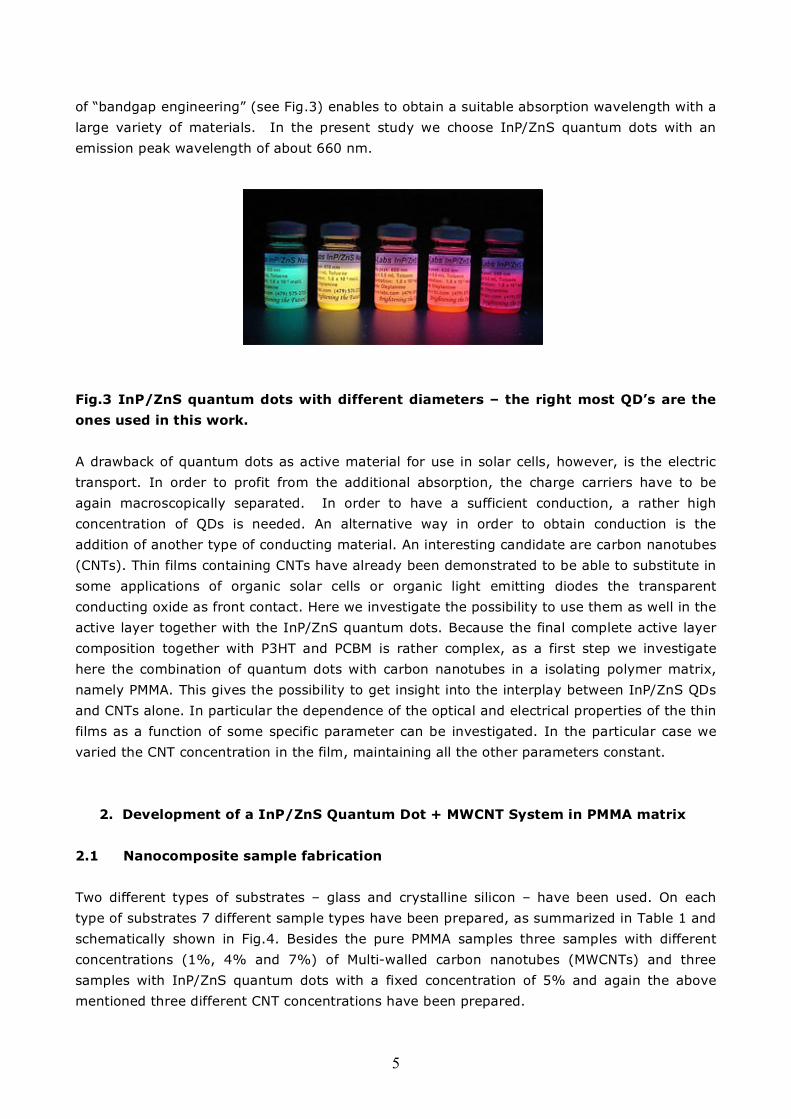
of “bandgap engineering” (see Fig.3) enables to obtain a suitable absorption wavelength with a
large variety of materials. In the present study we choose InP/ZnS quantum dots with an
emission peak wavelength of about 660 nm.
Fig.3 InP/ZnS quantum dots with different diameters – the right most QD’s are the
ones used in this work.
A drawback of quantum dots as active material for use in solar cells, however, is the electric
transport. In order to profit from the additional absorption, the charge carriers have to be
again macroscopically separated. In order to have a sufficient conduction, a rather high
concentration of QDs is needed. An alternative way in order to obtain conduction is the
addition of another type of conducting material. An interesting candidate are carbon nanotubes
(CNTs). Thin films containing CNTs have already been demonstrated to be able to substitute in
some applications of organic solar cells or organic light emitting diodes the transparent
conducting oxide as front contact. Here we investigate the possibility to use them as well in the
active layer together with the InP/ZnS quantum dots. Because the final complete active layer
composition together with P3HT and PCBM is rather complex, as a first step we investigate
here the combination of quantum dots with carbon nanotubes in a isolating polymer matrix,
namely PMMA. This gives the possibility to get insight into the interplay between InP/ZnS QDs
and CNTs alone. In particular the dependence of the optical and electrical properties of the thin
films as a function of some specific parameter can be investigated. In the particular case we
varied the CNT concentration in the film, maintaining all the other parameters constant.
2. Development of a InP/ZnS Quantum Dot + MWCNT System in PMMA matrix
2.1 Nanocomposite sample fabrication
Two different types of substrates – glass and crystalline silicon – have been used. On each
type of substrates 7 different sample types have been prepared, as summarized in Table 1 and
schematically shown in Fig.4. Besides the pure PMMA samples three samples with different
concentrations (1%, 4% and 7%) of Multi-walled carbon nanotubes (MWCNTs) and three
samples with InP/ZnS quantum dots with a fixed concentration of 5% and again the above
mentioned three different CNT concentrations have been prepared.
6
Table 1 Overview over the 14 different deposited samples types.
Fig.4 Schematics of the different produced samples.
The Polymethyl-methalacrylate (PMMA) powder was solved into Dimethylformamide (DMF) to
create the PMMA solution that has later been spin coated on the different substrates or served
as the basis for the more complex subsequent solutions with CNTs and QDs respectively. The
solution was then stirred for 30 min, resulting in a transparent and colourless solution
The preparation of the solution of PMMA with carbon nanotubes was done in the following way:
5mg of non functionalized MWCNTs were solved in 2ml of DMF inside a tube. The the tube was
sonicated for 30min at room temperature. For the 1% solution few CNT clusters were visible
and for the 4% and 7% solutions more clusters were visible in the otherwise homogeneously
black solution. In the next step the MWCNT solution was mixed with the PMMA solution in
order to obtain the three different concentrations of MWCNTs The three different solutions
were then sonicated for 60min at a temperature of 40°C.
Another set of tubes was processed the same way without sonication directly after the CNT
addition. These were used for the preparation of the solution containing either CNTs as well as
quantum dots. InP/ZnS quantum dots were added to this solutions with the three different
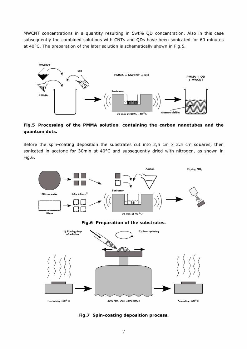
7
MWCNT concentrations in a quantity resulting in 5wt% QD concentration. Also in this case
subsequently the combined solutions with CNTs and QDs have been sonicated for 60 minutes
at 40°C. The preparation of the later solution is schematically shown in Fig.5.
Fig.5 Processing of the PMMA solution, containing the carbon nanotubes and the
quantum dots.
Before the spin-coating deposition the substrates cut into 2,5 cm x 2.5 cm squares, then
sonicated in acetone for 30min at 40°C and subsequently dried with nitrogen, as shown in
Fig.6.
Fig.6 Preparation of the substrates.
Fig.7 Spin-coating deposition process.
8
Subsequently the solutions were deposited on to the substrates by spin-coating with the
following parameters: single step with a speed of 2000rpm for 30s with an acceleration of
1500rpm/s. Before the spin-coating 0.3ml of solution was homogeneously distributed on the
substrates. Before applying this specific parameters the spin-coating process has been
optimized by varying the parameters using a purely PMMA in DMF solution in order to obtain a
homogeneous film with a thickness between 200nm and 300nm, as determined using a
profilometer. The samples were before and after spin-coating annealed for 2min at 170°C on a
hot plate. The spin-coating process is schematically shown in Fig.7.
2.2 Sample morphology
a) b)
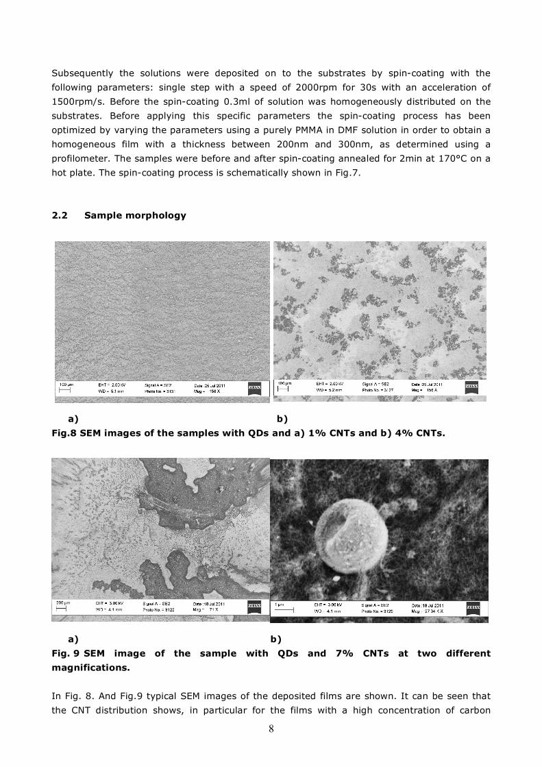
Fig.8 SEM images of the samples with QDs and a) 1% CNTs and b) 4% CNTs.
a) b)
Fig. 9 SEM image of the sample with QDs and 7% CNTs at two different
magnifications.
In Fig. 8. And Fig.9 typical SEM images of the deposited films are shown. It can be seen that
the CNT distribution shows, in particular for the films with a high concentration of carbon
9
nanotubes a rather inhomogeneous distribution is found. In the nanocomposite films with QDs
and 7% CNTs we observed a very particular feature, namely spheres with a diameter of about
3µm consisting of an agglomeration of carbon nanotubes. Probably either the quantum dots or
polymer spheres seem to act as a sort of seed for the formation of the spheres consisting of
CNTs.
2.3 Optical characterization of the solutions and of the nanocomposite films
During film processing the different solutions, used for the spin-coating preparation of the
samples, have been optically characterized, measuring the photoluminescence spectra. The
results are shown in the following figures.
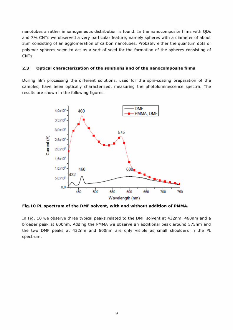
Fig.10 PL spectrum of the DMF solvent, with and without addition of PMMA.
In Fig. 10 we observe three typical peaks related to the DMF solvent at 432nm, 460nm and a
broader peak at 600nm. Adding the PMMA we observe an additional peak around 575nm and
the two DMF peaks at 432nm and 600nm are only visible as small shoulders in the PL
spectrum.
10
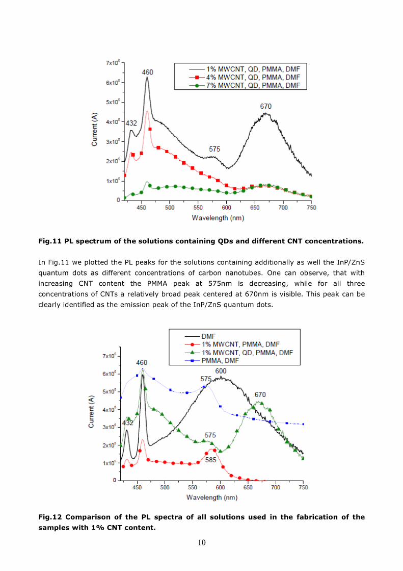
Fig.11 PL spectrum of the solutions containing QDs and different CNT concentrations.
In Fig.11 we plotted the PL peaks for the solutions containing additionally as well the InP/ZnS
quantum dots as different concentrations of carbon nanotubes. One can observe, that with
increasing CNT content the PMMA peak at 575nm is decreasing, while for all three
concentrations of CNTs a relatively broad peak centered at 670nm is visible. This peak can be
clearly identified as the emission peak of the InP/ZnS quantum dots.
Fig.12 Comparison of the PL spectra of all solutions used in the fabrication of the
samples with 1% CNT content.

11
In Fig.12 for comparison the PL spectra of all the solutions, used in the fabrication of the films
with 1% carbon nanotubes, are plotted together. One can clearly see that the 670nm peak is
present only in the quantum dot containing solution and not related to the carbon nanotubes.
The next photoluminescence spectra (Fig.13 and Fig.14) are measured on the nanocomposite
films. The y-axis, given in current, refers to the photocurrent of the detector used for the PL
measurements.
The results shown in Fig.13 are measured on the deposited films containing quantum dots and
1% MWCNTs. We see basically the broad red emission peak at 670nm with a FWHM value of
67nm, related to the quantum dot emission. This confirms the successful incorporation of the
quantum dots into the deposited films. This emission peak could, however, only be observed
on the sample with a low content of carbon nanotubes (see Fig.14). A possible explanation for
this suppression of the QD photoluminescence with increasing CNT content is that the
nanotubes are optically shielding the quantum dots, for example by the formation of the
spheres, observed in Fig.9. Another explanation would be the quenching of the PL by efficient
charge carrier separation. It is for example well known, that the photoluminescence of P3HT is
quenched by the addition of the fullerenes.
Fig.13 Comparison of the PL spectra of the nanocomposite film with 1%MWCNTs and
5%QDs, deposited on different substrates.
12
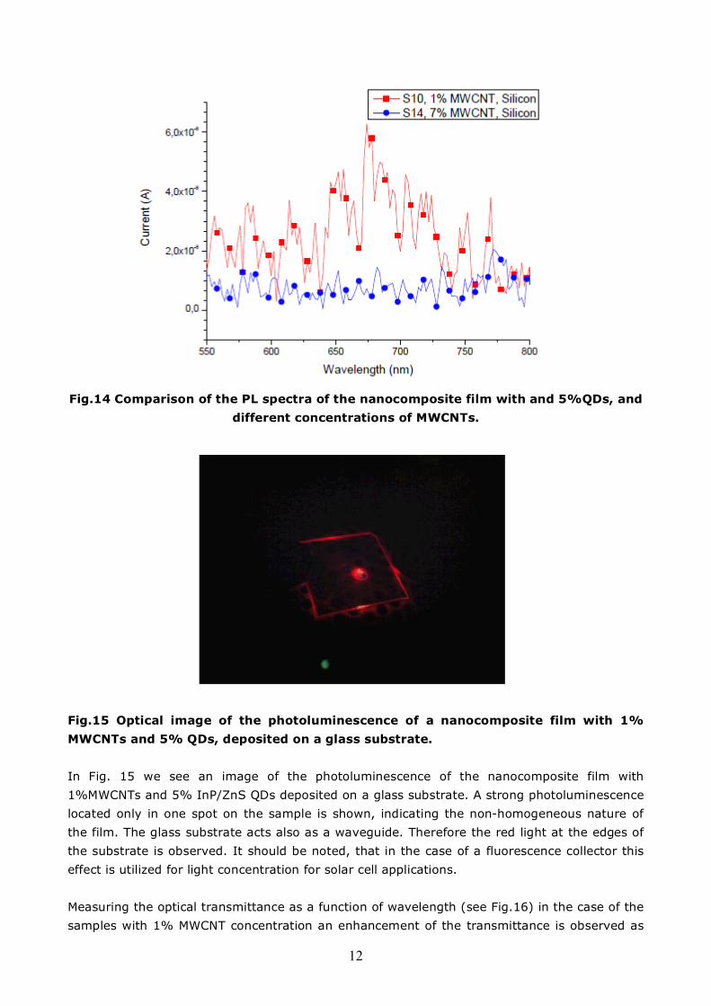
Fig.14 Comparison of the PL spectra of the nanocomposite film with and 5%QDs, and
different concentrations of MWCNTs.
Fig.15 Optical image of the photoluminescence of a nanocomposite film with 1%
MWCNTs and 5% QDs, deposited on a glass substrate.
In Fig. 15 we see an image of the photoluminescence of the nanocomposite film with
1%MWCNTs and 5% InP/ZnS QDs deposited on a glass substrate. A strong photoluminescence
located only in one spot on the sample is shown, indicating the non-homogeneous nature of
the film. The glass substrate acts also as a waveguide. Therefore the red light at the edges of
the substrate is observed. It should be noted, that in the case of a fluorescence collector this
effect is utilized for light concentration for solar cell applications.
Measuring the optical transmittance as a function of wavelength (see Fig.16) in the case of the
samples with 1% MWCNT concentration an enhancement of the transmittance is observed as
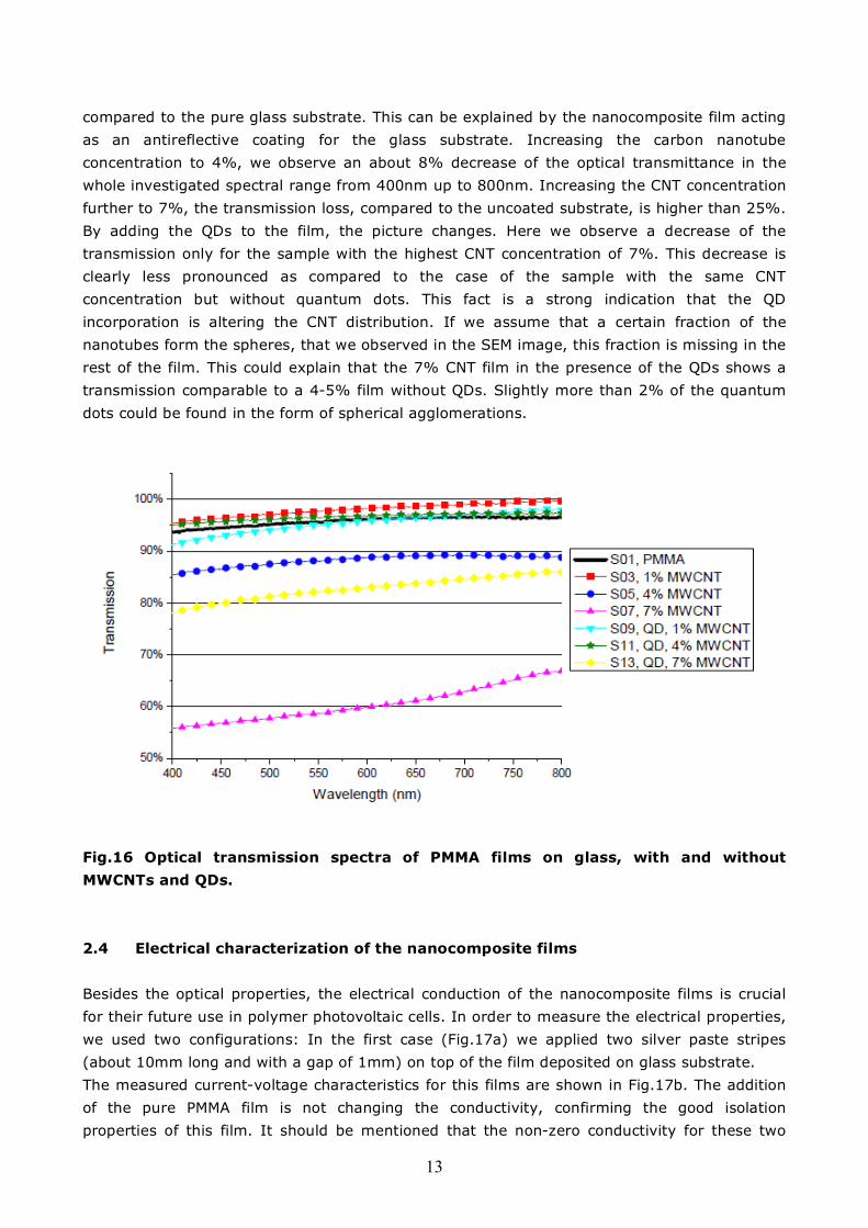
13
compared to the pure glass substrate. This can be explained by the nanocomposite film acting
as an antireflective coating for the glass substrate. Increasing the carbon nanotube
concentration to 4%, we observe an about 8% decrease of the optical transmittance in the
whole investigated spectral range from 400nm up to 800nm. Increasing the CNT concentration
further to 7%, the transmission loss, compared to the uncoated substrate, is higher than 25%.
By adding the QDs to the film, the picture changes. Here we observe a decrease of the
transmission only for the sample with the highest CNT concentration of 7%. This decrease is
clearly less pronounced as compared to the case of the sample with the same CNT
concentration but without quantum dots. This fact is a strong indication that the QD
incorporation is altering the CNT distribution. If we assume that a certain fraction of the
nanotubes form the spheres, that we observed in the SEM image, this fraction is missing in the
rest of the film. This could explain that the 7% CNT film in the presence of the QDs shows a
transmission comparable to a 4-5% film without QDs. Slightly more than 2% of the quantum
dots could be found in the form of spherical agglomerations.
Fig.16 Optical transmission spectra of PMMA films on glass, with and without
MWCNTs and QDs.
2.4 Electrical characterization of the nanocomposite films
Besides the optical properties, the electrical conduction of the nanocomposite films is crucial
for their future use in polymer photovoltaic cells. In order to measure the electrical properties,
we used two configurations: In the first case (Fig.17a) we applied two silver paste stripes
(about 10mm long and with a gap of 1mm) on top of the film deposited on glass substrate.
The measured current-voltage characteristics for this films are shown in Fig.17b. The addition
of the pure PMMA film is not changing the conductivity, confirming the good isolation
properties of this film. It should be mentioned that the non-zero conductivity for these two

14
samples are due to the conductivity of the glass substrate. For all three nanocomposite films,
however, we observe a clear increase of the conductivity, but not in a monotonic way with the
CNT content. The smallest conductivity increase is found for the 1%CNT sample, the highest
one for the 4%CNT sample and an intermediate value for the 7% CNT sample. This non-
monotonic behavior can be eventually explained by the increasing inhomogeneity of the
sample with increasing CNT content, as observed in the SEM images. Therefore the effective
formation of a percolation network is not reached for the 7% sample. All measured
characteristics in sandwich configuration were symmetric and only in the case of the 4%CNT
containing film we observed a small hysteresis in the current-voltage characteristics for
negative applied voltages.
a) b)
Fig 17 Current-voltage characteristics measured for the films with and without
different concentrations of CNTs in coplanar configuration.
a) b)
Fig 18 Current-voltage characteristics measured for the films with and without
different concentrations of CNTs in sandwich configuration.
In order to test the vertical electrical transport, we performed an electrical characterization in
sandwich configuration, where the films have been deposited on crystalline silicon (see
15
Fig.18a). The resulting current-voltage characteristics are shown in Fig.18b. Again very low
conduction is found for the pure PMMA film. Increasing the CNT concentration of the film, we
see the formation of a diode like behavior of the samples, with a asymmetric current-voltage
characteristics. The forward bias direction is found for positive voltages applied to the top
contact as referred to the bottom back contact on the crystalline silicon. With increasing CNT
concentration the onset voltage for conduction decreases monotonically down to a value of
about 0.5V in the case of the sample with a 7% CNT concentration. The system can be
modelled as a type of Schottky diode, where the silicon substrate plays the role of the
semiconductor, while the MWCNTs act as metallic contact. The resulting I-V characteristics is
therefore enabling to give an estimation of the effective vertical conduction in the
nanocomposite layer. For a more detailed analysis in the future, temperature dependent
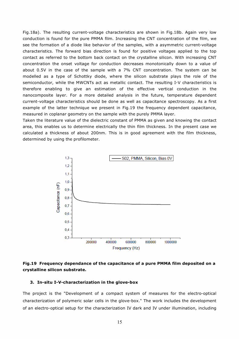
current-voltage characteristics should be done as well as capacitance spectroscopy. As a first
example of the latter technique we present in Fig.19 the frequency dependent capacitance,
measured in coplanar geometry on the sample with the purely PMMA layer.
Taken the literature value of the dielectric constant of PMMA as given and knowing the contact
area, this enables us to determine electrically the thin film thickness. In the present case we
calculated a thickness of about 200nm. This is in good agreement with the film thickness,
determined by using the profilometer.
Fig.19 Frequency dependance of the capacitance of a pure PMMA film deposited on a
crystalline silicon substrate.
3. In-situ I-V-characterization in the glove-box
The project is the "Development of a compact system of measures for the electro-optical
characterization of polymeric solar cells in the glove-box." The work includes the development
of an electro-optical setup for the characterization IV dark and IV under illumination, including

16
the implementation of software for instrument control and for the extrapolation of the
parameters of the solar cells.
The introduction of a compact measuring system inside the glove-box, environment of
controlled atmosphere with low oxygen and moisture, allows to characterize the solar cells
before degradation.
The measurement setup is shown in Fig.20 and consists of a Personal Computer with
Fig.20 Measurement setup for characterizing electro-optical to be inserted in the
glove-box.
PCI-GPIB interface, by a Keithley 2400 SourceMeter, by a xenon lamp Lot Oriel LSN251, by a
test equipment HP 16055A, by a four probes and a fiber optics. The software part was
implemented using Labview 7.1.
The characterization procedure is divided in two parts:
• Analysis IV using the 2-wire mode sense;
• Analysis IV under illumination via 4-wire sense mode with extrapolation of the
parameters.
In both cases the SourceMeter, remotely controlled via Labview, supplies a voltage and
measuring a current. It is also possible to make a dark analysis using the 4 wire sense mode,
Fig.21.

17
Fig.21 Screenshot of software index.
3.1 I-V dark analysis (2-wire sense)
The measurement setup is shown in Fig. 23, where the front contact of a solar cell is
connected to the positive test lead (+) and the back-contact to the tip negative (-).
Fig.23 Measurement setup for the I-V dark.
18
The HP 16055A test equipment provides an electrostatic shield and prevents light to excite the
device for a stable measurement of the current order of pA. The maximum applicable voltage
is ± 200 V DC
Using 2-wire sense mode, it requires a voltage that varies from a minimum to a maximum
value at a given step and measure the current. In this procedure require that the voltage test
leads are the same as the current measure. With the use of Reverse Mode is possible to
analyze the Dark IV characteristic to study a possible hysteresis in the device.
The code snippet sent to 2400 SourceMeter via GPIB is follows:
*RST
:SYST:AZER:STAT ON
:SYST:BEEP:STAT 0
In this way the instrument is reset and is ready for the next measurement.
:SOUR:FUNC VOLT
:SOUR:VOLT:MODE FIX
:SOUR:VOLT:RANG 10
:SOUR:VOLT:LEV 2.000000
The instrument is set as a source of tension to be applied to the device, defining the working
range, the level of tension and the ways in which the voltage must be applied.
:SENS:CURR:PROT 1050E-3
:SENS:FUNC "CURR"
:SENS:CURR:RANG:AUTO ON
:FORM:ELEM CURR
The instrument is set to measure the current, setting the compliance equal to 1.05 A, it also
enables the instrument to interpret the characters in the input buffer as current values .
:OUTP ON
:READ?
The code sets the imposed voltage and measuring the current.
At the end of the measuring procedure the applied voltage is disabled by the command
:OUTP OFF
to ensure an adequate safety level to the operator.
The software "J-V Dark 2 wire" creates a default folder in C: \ I_V_Measures \ Dark_2_ wire
and saves all the data in text files.
19
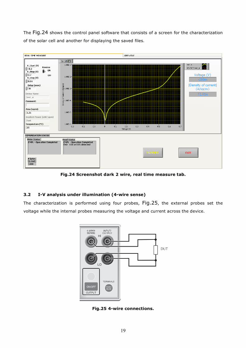
The Fig.24 shows the control panel software that consists of a screen for the characterization
of the solar cell and another for displaying the saved files.
Fig.24 Screenshot dark 2 wire, real time measure tab.
3.2 I-V analysis under illumination (4-wire sense)
The characterization is performed using four probes, Fig.25, the external probes set the
voltage while the internal probes measuring the voltage and current across the device.
Fig.25 4-wire connections.
20
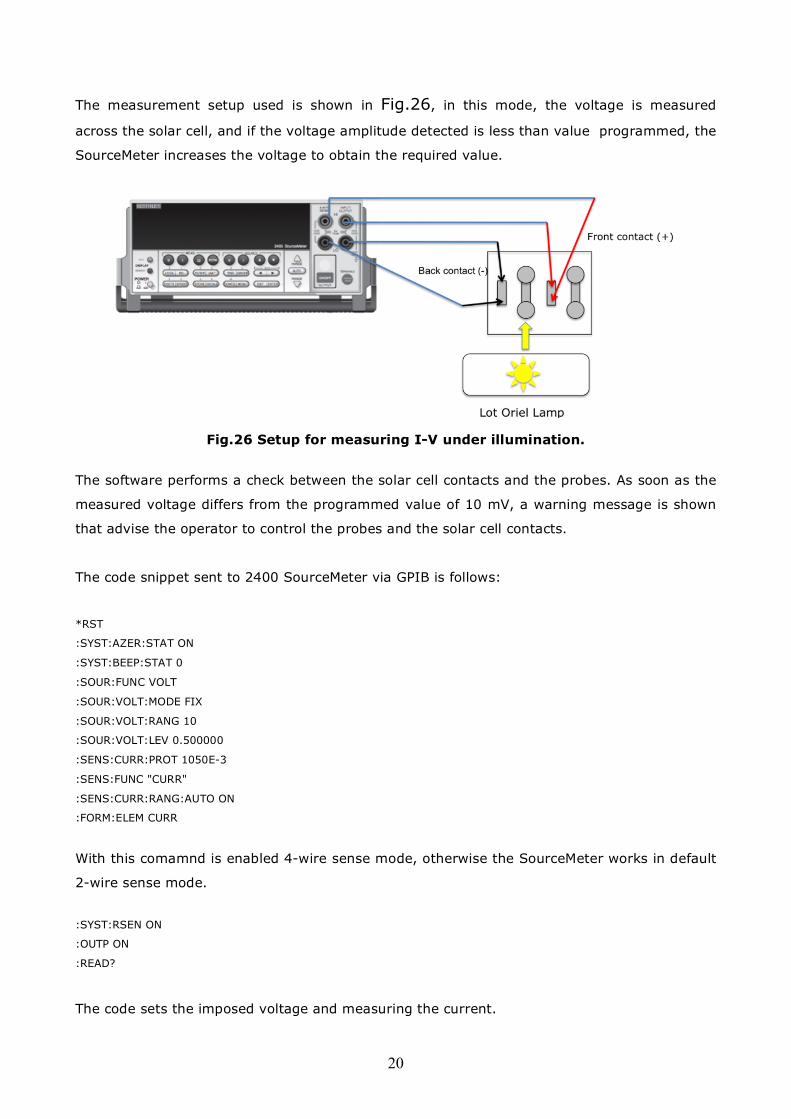
The measurement setup used is shown in Fig.26, in this mode, the voltage is measured
across the solar cell, and if the voltage amplitude detected is less than value programmed, the
SourceMeter increases the voltage to obtain the required value.
Fig.26 Setup for measuring I-V under illumination.
The software performs a check between the solar cell contacts and the probes. As soon as the
measured voltage differs from the programmed value of 10 mV, a warning message is shown
that advise the operator to control the probes and the solar cell contacts.
The code snippet sent to 2400 SourceMeter via GPIB is follows:
*RST
:SYST:AZER:STAT ON
:SYST:BEEP:STAT 0
:SOUR:FUNC VOLT
:SOUR:VOLT:MODE FIX
:SOUR:VOLT:RANG 10
:SOUR:VOLT:LEV 0.500000
:SENS:CURR:PROT 1050E-3
:SENS:FUNC "CURR"
:SENS:CURR:RANG:AUTO ON
:FORM:ELEM CURR
With this comamnd is enabled 4-wire sense mode, otherwise the SourceMeter works in default
2-wire sense mode.
:SYST:RSEN ON
:OUTP ON
:READ?
The code sets the imposed voltage and measuring the current.
21
Afterwards the instrument is enabled to impose voltage and voltage measuring sending the
following code:
:SENS:FUNC "VOLT"
:SENS:CURR:RANG:AUTO ON
:FORM:ELEM VOLT
:SYST:RSEN ON
:OUTP ON
:READ?
At the end of the measuring procedure the applied voltage is disabled by the command
:OUTP OFF
to ensure an adequate safety level to the operator.
The software "J-V Light 4 wire" creates a default folder in C: \ I_V_Measures \ Light_4_ wire
and saves all the data in text files.
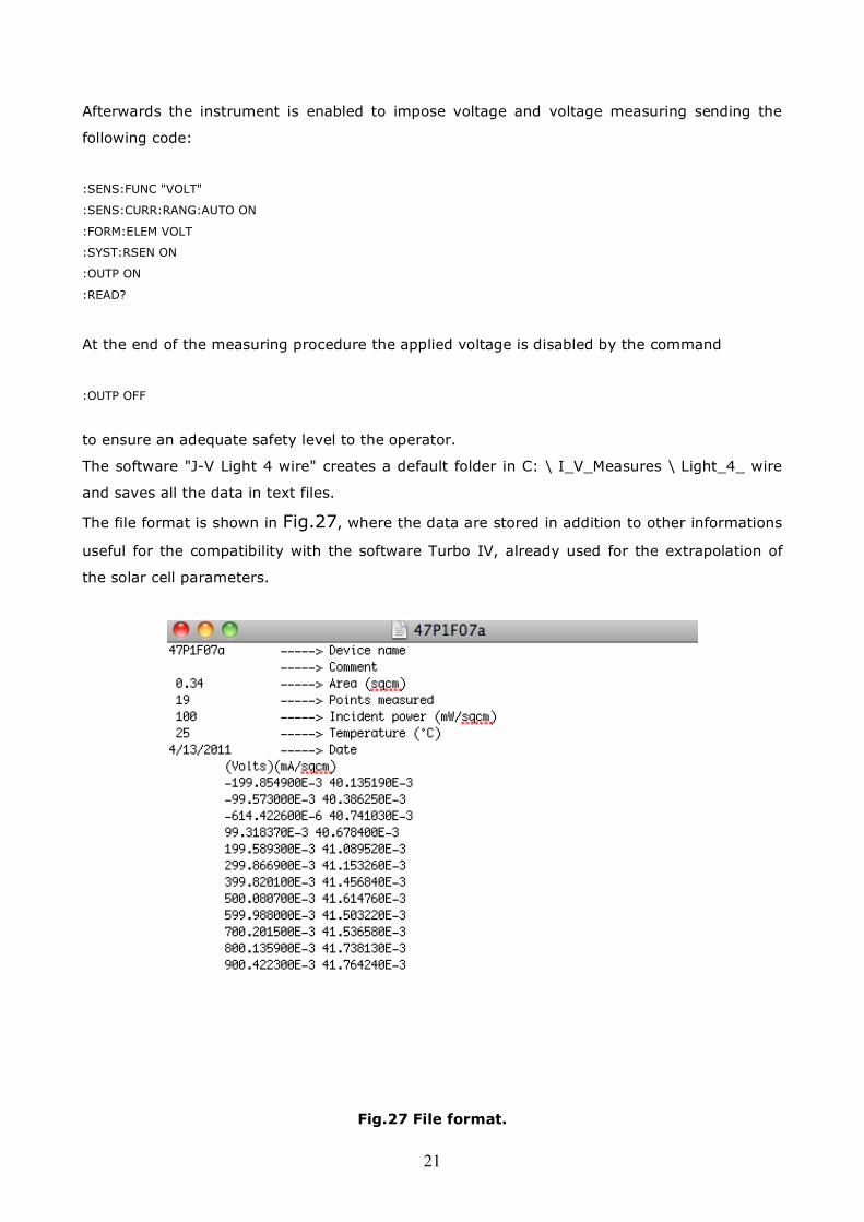
The file format is shown in Fig.27, where the data are stored in addition to other informations
useful for the compatibility with the software Turbo IV, already used for the extrapolation of
the solar cell parameters.
Fig.27 File format.
22
To ensure a correct extrapolation of the solar cell parameters, the light source consists of a
lamp Lot Oriel 300 W LSN251, an optical fiber and a lens, should be characterized in terms of
the spectral matching compared of the sun spectra AM 1.5, and spatial uniformity across the
illuminated1 area equal to 100 mW/cm2.
By placing the solar cell at a distance of 4 cm from the light source, and making a direct
measurement of the incident power, the value of 100 mW/cm2 at the solar cell surface is
obtained.
Through the calculation of the mismatch factor M it is obtained the class of the light source and
a measure of how its spectrum is different from AM 1.5 spectra. Every small change has an
impact on an error of the short circuit current Isc.
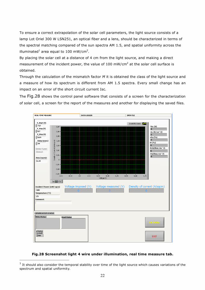
The Fig.28 shows the control panel software that consists of a screen for the characterization
of solar cell, a screen for the report of the measures and another for displaying the saved files.
Fig.28 Screenshot light 4 wire under illumination, real time measure tab.
1It should also consider the temporal stability over time of the light source which causes variations of the spectrum and spatial uniformity.
23
4 Conclusions
Within the frame work of this project a new nanocomposite film, based on the combination of
InP/ZnS quantum dots for enhanced optical absorption in the red part of the solar spectrum
and of multi-walled carbon nanotubes for the increase of the thin film electrical conductivity
has been developed using the spin-coating deposition technique. As a matrix for the test of
this new combination of nanoparticles electrically non-conducting PMMA has been used. The
measurement of the morphology of the films by SEM imaging and of the optical properties by
photoluminescence and transmittance revealed a rather complex interplay between nanotubes
and quantum dots. In particular, there we found a strong tendency of the nanotubes in the
case of a high concentration of CNTs to agglomerate in spherical configuration. Electrical
conductivity measurements in coplanar and sandwich configuration enabled to verify the
degree of increase of the sample conductivity by the nanotube addition. In particular the
measurements in sandwich configuration revealed the formation of a Schottky diode type
behavior in a structure where the PMMA/CNT film has been deposited directly on a crystalline
silicon substrate. The homogeneity of the films is still poor, which has been for example
revealed by photoluminescence imaging.
The authors want to thank Carmela Borriello, Tiziana di Luccio, Pasquale Morvillo ed Anna De
Girolamo Del Mauro