
Semi-empirical and ab-initio calculations of...
166
UNIVERSIT ` A DEGLI STUDI DI PAVIA Facolt` a di Scienze Matematiche Fisiche e Naturali Dipartimento di Fisica “A. Volta” Semi-empirical and ab-initio calculations of optical properties in semiconductor superlattices Silvana Botti Tesi presentata per il conseguimento del titolo di Dottore di Ricerca in Fisica XIV CICLO
Transcript of Semi-empirical and ab-initio calculations of...
UNIVERSITA DEGLI STUDI DI PAVIA
Facolta di Scienze Matematiche Fisiche e Naturali
Dipartimento di Fisica “A. Volta”
Semi-empirical and ab-initio
calculations of optical properties in
semiconductor superlattices
Silvana Botti
Tesi presentata per il conseguimento del
titolo di Dottore di Ricerca in Fisica
XIV CICLO

Coordinatore del dottorato di ricerca in fisica
presso l’Universita di Pavia:
Prof. S. P. Ratti
Tutore nelle attivita di ricerca:
Prof. L.C. Andreani
Io vedo le teorie scientifiche come costruzioni umane
– reti progettate da noi per catturare il mondo.
(K. Popper)
A mio padre

4
Table of contents
1 Introduction and overview 7
2 Semi-empirical calculations of superlattice band structures 15
2.1 The choice of an empirical model . . . . . . . . . . . . . . . . . . . . 16
2.2 The Linear Combination of Bulk Bands method . . . . . . . . . . . . 18
2.3 From bulk to superlattice states . . . . . . . . . . . . . . . . . . . . . 23
2.4 Calculated superlattice electronic levels . . . . . . . . . . . . . . . . . 31
3 Ab-initio calculations of superlattice band structures 39
3.1 Density Functional Theory . . . . . . . . . . . . . . . . . . . . . . . . 40
3.1.1 The Hohenberg-Kohn theorem . . . . . . . . . . . . . . . . . . 41
3.1.2 The Kohn-Sham scheme . . . . . . . . . . . . . . . . . . . . . 42
3.1.3 The Local Density Approximation . . . . . . . . . . . . . . . . 45
3.2 Technical aspects . . . . . . . . . . . . . . . . . . . . . . . . . . . . . 47
3.2.1 Plane wave basis . . . . . . . . . . . . . . . . . . . . . . . . . 47
3.2.2 Sets of k-points for integration over the Brillouin zone . . . . 48
3.3 Results for ground-state properties . . . . . . . . . . . . . . . . . . . 49
3.4 Kohn-Sham eigenstates and quasi-particle states . . . . . . . . . . . . 52
3.5 Bulk band structure by DFT-LDA calculations . . . . . . . . . . . . . 56
3.6 Superlattice band structure by DFT-LDA calculations . . . . . . . . . 62
4 Semi-empirical calculations of optical properties 69
4.1 Semi-classical theory of interband transitions . . . . . . . . . . . . . . 72
4.2 Results for bulk optical spectra . . . . . . . . . . . . . . . . . . . . . 78
4.3 Optical spectra for GaAs/AlAs and GaAs/vacuum superlattices . . . 80
5

6
4.4 Optical anisotropy and macroscopic dielectric tensor . . . . . . . . . . 84
4.5 Calculations of birefringence . . . . . . . . . . . . . . . . . . . . . . . 87
5 Ab-initio calculations of optical properties 93
5.1 Time Dependent Density Functional Theory . . . . . . . . . . . . . . 96
5.1.1 Derivation of an expression for the dielectric function . . . . . 98
5.1.2 RPA approximation without local field effects . . . . . . . . . 100
5.2 Local field effects . . . . . . . . . . . . . . . . . . . . . . . . . . . . . 102
5.3 Results for the birefringence of GaAs/AlAs superlattices . . . . . . . 103
5.4 Effects of the long-range contribution to the xc kernel on the bulk
spectra . . . . . . . . . . . . . . . . . . . . . . . . . . . . . . . . . . . 114
6 Summary and discussion 125
A Basic approximations 131
B Pseudopotentials 135
B.1 What a pseudopotential is . . . . . . . . . . . . . . . . . . . . . . . . 135
B.2 Empirical pseudopotentials . . . . . . . . . . . . . . . . . . . . . . . . 138
B.3 Ab-initio pseudopotentials . . . . . . . . . . . . . . . . . . . . . . . . 143
B.3.1 Hamann pseudopotentials . . . . . . . . . . . . . . . . . . . . 143
B.3.2 Troullier and Martins pseudopotentials . . . . . . . . . . . . . 150
B.3.3 Kleinman-Bylander formulation . . . . . . . . . . . . . . . . . 151
B.4 The norm-conserving pseudopotentials built to be used in this work . 153
Bibliography 155
Ringraziamenti 166

Chapter 1
Introduction and overview
A semiconductor heterostructure is an artificial material, basically obtained by epi-
taxial growth and/or chemical etching of two or more different semiconductors. The
size reduction achieved in one, two or three dimensions in heterostructures at the
nanoscale level leads to electronic ground and excited states widely different from
those of the bulk crystals, and has opened the way to a new generation of optoelec-
tronic and photonic devices.
If we consider the evolution of an electronic state from a bulk crystal to a nanos-
tructure, essentially three phenomena occur. First, the band-offsets at the interfaces
act as effective potential barriers, which confine the carriers, both the electrons and
the holes, in one, two or three dimensions. Second, for an artificial periodic system,
e.g. a superlattice, the supercell is made up by joining a number Nc of primitive cells
of the underlying bulk lattices. Hence, in the reciprocal space Nc k-points in the
Brillouin zone of the bulk are folded onto the same k-point in the smaller Brillouin
zone of the nanostructure, and the artificially superimposed potential induces a cou-
pling between previously independent bulk states. Third, the artificial combination
of different materials usually leads to a reduction of the originally higher symmetry
of the constituent bulk materials.
Quantum confinement and confinement-induced mixing affect the energy and the
dimensionality of electronic levels, the lowering in the crystal symmetry is responsi-
ble for the removal of level degeneracies. In practice, to take advantage of all these
modifications in the electronic states, we have to consider how they are reflected in
7
8 Chapter 1. Introduction and overview
modifications of the quantities of interest. In particular, the optical properties are
of the utmost importance, as they lie at the basis of many new technological appli-
cations. Among the already well-established applications we can cite the multiple
quantum well (MQW) lasers [1, 2], the quantum cascade lasers [3], the Schottky
barriers [1, 2], the modulation-doped heterostructures [1, 2], like the high electron
mobility transistors (HEMT). Dielectric superlattices are developed for their non-
linear properties, which induce effects such as the optical bistability or the nonlinear
frequency conversion [4]. Those effects are also found in semiconductor heterostruc-
tures based on GaAs, which has by itself important nonlinear optical properties [5].
The optical bistability has for instance been observed in a photoexcited GaAs/AlAs
superlattice [6]. In search of new optical sources, in GaAs/oxidized-AlAs super-
lattices the optical anisotropy has been exploited to achieve phase matching for
second-harmonic generation, the enhanced dielectric contrast has produced a break-
through in the construction of Bragg reflectors for MQW lasers and microcavities
and birefringent waveguides have been proposed [7].
Let us analyze more in details the physical effects involved in the above mentioned
applications. Interband absorption spectra of bulk tetrahedral semiconductors (like
Silicon, GaAs, AlAs, . . .) are dominated by two prominent features, denoted E1 and
E2 [8, 9]. The E1 peak originates from band-to-band transitions along the Γ − L
direction, where valence and conduction bands are nearly parallel: this results in
a M1-type critical point, i.e. a saddle point in the joint density of states, which
also gives a strong excitonic character to the transition. The E2 peak, instead, has
contributions from different parts of the Brillouin zone, but mainly from a region
centered around the special point (34, 1
4, 1
4) (in units of 2π/a, where a is the lattice
constant). Starting from a basic level of analysis, in a nanostructure the confine-
ment of the carriers, as the simplistic exercise of the particle in a box can teach,
leads to a blue shift and a sharpening of the absorption peaks. In addition, re-
moval of level degeneracies can induce the subdivision of the transitions in groups,
leading to splittings of the absorption peaks. In the past, most experimental inves-
tigations have focused on the energy region of the fundamental gap, which is easily
accessible by photoluminescence and photoluminescence excitation spectroscopies
and yields a variety of interesting physical phenomena related to bound excitonic

9
states. Relatively few studies of confinement effects on high-energy transitions have
been presented. Blue shifts and splittings of the E1 and E2 transitions were mea-
sured in GaAs/AlAs superlattices [10, 11]. More recently, a quantum confinement
induced shift of E1 and E2 was measured in Ge nanoparticles embedded in a glassy
matrix [12, 13]. Concerning theory, confined electronic levels close to band edges,
excitonic effects and the resulting optical properties can be calculated rather simply
and accurately by the envelope-function method [14]. The theoretical problem of
determining optical spectra of semiconductor heterostructures in the whole visible
region is much more complex and beyond the reach of effective-mass methods, as it
requires a description of the effects of confinement and coupling on electronic states
in the whole Brillouin zone.
Yet, there is still a remarkable effect of the reduction of symmetry to be consid-
ered, which obliges us to move to a deeper level of analysis of the problem. The
original point group of most of the bulk semiconductors which constitute the studied
heterostructures is the cubic group of the diamond or zinc-blend structure, which
yields an isotropic optical response of the medium. The lowering in the crystal
symmetry gives rise to an optical anisotropy in the real part of the dielectric con-
stant (birefringence) and in the imaginary part (absorption anisotropy or dichroism).
Even at zero-frequency, birefringence can be large, like in nanostructured silicon sur-
faces [15], or of moderate amplitude, as in GaAs/AlAs superlattices [16], where it
also shows a non-trivial dependence on the superlattice period. The basic picture
in terms of transitions between one-electron states, mainly used up to now, ignores
contributions from many-body effects which may play a crucial role, and which tend
to be especially important when the scale of the system is reduced and the inhomo-
geneity of the medium is more pronounced. Self-energy and electron-hole interaction
(i.e. excitonic) effects can have a significant contribution to the absorption spectra
of even simple bulk semiconductors. The former corrects the ground state exchange-
correlation potential, the latter describes the variations of the exchange-correlation
potential upon excitation. Of course, there are also contributions stemming from
variations of the Hartree potential, including the so-called local field effects, which
express the fact that these variations reflect the charge inhomogeneity of the re-
sponding material. Therefore, local field effects can be of moderate importance,

10 Chapter 1. Introduction and overview
compared to the exchange-correlation contributions, in the absorption spectra of
simple bulk semiconductors, but show up increasingly when one considers more
inhomogeneous systems.
Most of the today technologically interesting systems are strongly inhomoge-
neous, and their potential applications might even be based on their inhomogeneity
- superlattices are one of the best examples. As a first conclusion, we can now
designate the nearly lattice-matched GaAs/AlAs superlattices as the ideal proto-
type systems for the understanding of artificial structures. Many reference data
are available, since their optical properties have been thoroughly investigated both
experimentally [10, 17, 18] and theoretically [19, 20, 21, 22, 23, 24, 25]. In this
thesis we will study the electronic states all over the Brillouin zone and the optical
properties, with a special care for the optical anisotropy, of two specific kinds of
systems: (GaAs)p/(AlAs)p superlattices and free-standing GaAs layers, which are
simulated by (GaAs)p/(vacuum)p superlattices. Both these systems consist in the
periodic alternation of layers of two different materials (or also an empty lattice)
with an original zinc-blend structure. Each layer is composed by the same number
p of (001) planes: 2p planes compose the supercell. An example of GaAs/AlAs
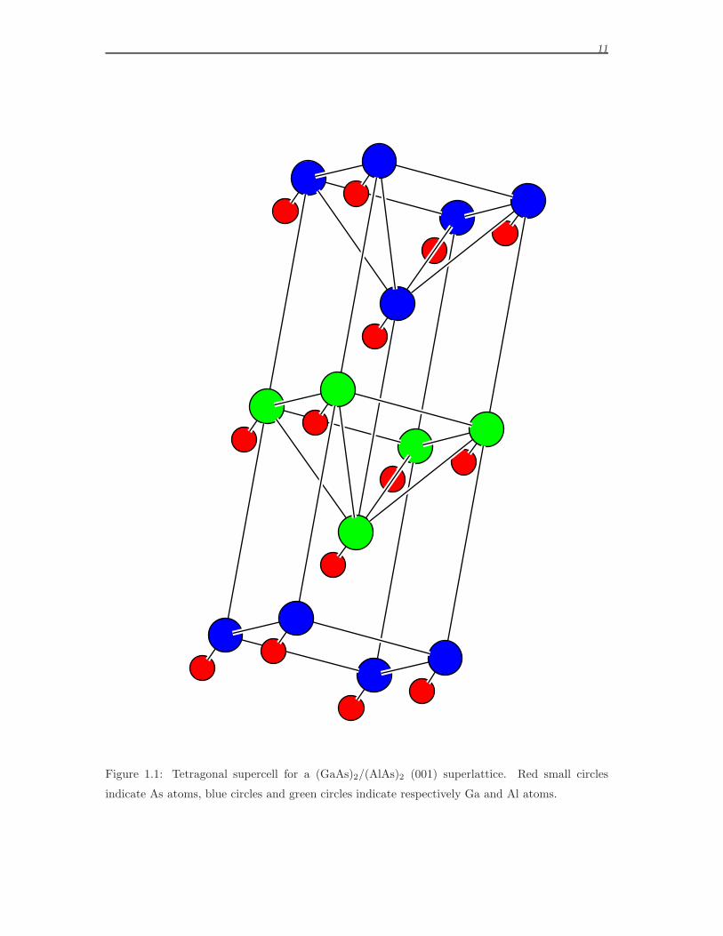
tetragonal supercell is shown in Fig. 1.1 on page 11. Besides the obvious choice of
GaAs/AlAs systems, the motivation for studying GaAs/vacuum superlattices is to
analyze how confinement effects act in a system where the electronic states are truly
confined in GaAs layers, even at high energies. In GaAs/AlAs superlattices, in fact,
the band structures of the two constituents far away from the fundamental band
edges are rather similar and strong banding effects occur in short-period structures,
i.e. the electronic states become delocalized along the superlattice. A comparison
between the two systems should therefore elucidate the respective roles of quantum
confinement and superlattice band formation in determining the optical properties.
However, free-standing GaAs films are not only an ideal model system, as they can
be produced by chemical etching [26], and, moreover, GaAs/vacuum superlattices
can be a model for superlattices made of GaAs and a wide-gap oxide, like Al2O3 or
oxidized AlAs (AlOx).
GaAs/AlAs superlattices have been the subject of various theoretical studies.
Most of the approaches well established for bulk band structure calculations reveal
11
Figure 1.1: Tetragonal supercell for a (GaAs)2/(AlAs)2 (001) superlattice. Red small circles
indicate As atoms, blue circles and green circles indicate respectively Ga and Al atoms.
12 Chapter 1. Introduction and overview
some weaknesses, when applied to a low-dimensional system. A completely satisfac-
tory method should describe accurately, all over the Brillouin zone, both intervalley
coupling and confinement effects, in systems of any scale, constituted by few-atom
to million-atom supercells. In literature, only the electronic structure of very-short-
period (GaAs)p/(AlAs)p superlattices has been calculated from first principles by
Density Functional Theory (DFT) and norm-conserving pseudopotentials (see Sec-
tion 3.5). DFT calculations benefit of a high degree of precision, which cannot be
reached by empirical calculations. Nevertheless, the computation time grows rapidly
with the number p of monolayers, making the method impractical for large scale sys-
tems. Thus, many empirical methods have been developed in the last decades to
study large-scale superlattices (see Section 2.1). While reaching a simplification of
the problem, they often fail to describe correctly all the physical effects involved.
Concerning the optical properties, only a few calculations of absorption spectra
for very-small period superlattices exist. Moreover, very few information is known
about the dielectric properties and the anisotropy at zero frequency of GaAs/AlAs
superlattices. First, the refractive index has been neither measured nor calculated,
and it is commonly estimated from the dielectric constants of bulk GaAs and AlAs
in the framework of the effective medium approach [27]. This classical theory may
fail for small period superlattices, where the delocalization of the electronic states
over the superlattice implies that the use of the bulk dielectric constants is not
justified anymore. In fact, theoretical calculations have shown for ultrathin (001)
(GaAs)p/(AlAs)p SL’s that an effective medium model cannot explain the behav-
ior from p=1 to p=3 [11]. Second, the change in the refractive index with light
polarization – the static birefringence – has been measured for large period (001)
(GaAs)p/(AlAs)p SL’s and a remarkable drop has been observed (see Fig 4.9 on page
90) as the period decreases. This behavior has been suggested to depend on local
fields [16]. Ab initio methods for ultrathin SL’s [11], and a semi-empirical approach
for larger ones [28], have been applied neglecting local field effects and did not ac-
count for the observed value of the birefringence, nor for its decrease with decreasing
p, even qualitatively.
After having defined the systems we are going to study, and after clarifying the
reasons for their interest and the variety of physical phenomena that they show, we
13
want to discuss the objectives of this thesis work. We aim at attaining:
(i) A detailed analysis of the electronic band structure of superlattices; in partic-
ular a comprehension of how different physical effects, i.e. confinement, super-
lattice potential-induced couplings, lowering of crystal symmetry, influence the
evolution from the bulk electronic states to the superlattice states.
(ii) An insight in the advantages and disadvantages and an instructive comparison
of two powerful models for electronic calculations in solids, namely the pseu-
dopotential Linear Combination of Bulk Bands (LCBB) method [29] and the
Density Functional Theory (DFT), used in the Local Density Approximation
(LDA), with norm-conserving pseudopotentials and a plane wave basis set. The
first of them is based on a semi-empirical parameterization of the pseudopoten-
tial, which involves a fitting on experimental data, the second relies completely
on first principles. Concerning the LCBB method, we have developed a code
based on this method to study superlattice states and optical properties.
(iii) A detailed determination of the dielectric properties of superlattices, both in
the isotropic approximation and considering the anisotropy of the dielectric
tensor for light polarizations along growth or in-plane directions. We will focus
on the behavior under confinement of the peaks in the absorption curves and
on the anisotropy of the optical response, in particular calculating the dielectric
tensor components and the zero-frequency birefringence. These properties will
be analyzed as a function of the superlattice period p. Once again, the discus-
sion will follow the two parallel roads of a semi-empirical and a first-principle
Time-Dependent DFT (TDDFT) approach to the problem. The two methods
will be applied, on one hand, within the same approximation, to judge the
consistency of the corresponding results. On the other hand, we will try to
differentiate the calculations in order to cast light on all the possible physical
effects presented above. As a first step, we will discuss to what extent confine-
ment and folding-induced modifications on the electronic states are sufficient
in reproducing experimental data. This kind of analysis will be carried out in
a semi-empirical approach, within the semplified picture of Fermi’s golden rule
for one-particle states and independent particle transitions. Afterwards, we will
14 Chapter 1. Introduction and overview
compare the obtained results with totally analogous independent-transition ab
initio calculations. Then, we will introduce local field effects in the ab initio
TDDFT calculations, to understand whether they give a relevant contribution
to the optical anisotropy, as it can be expected intuitively. We will finally
conjecture, in view of the obtained results, how many-body effects can further
contribute to the results. We will test two different approximations (RPA and
TDLDA) for the inclusion of the exchange-correlation contributions. To in-
clude quasi-particle and excitonic effects, within a many-body Green’s function
formulation is out of reach for the existing computational tools, except in case
of very-thin superlattices.
(iv) An innovative investigation of the optical spectra of bulk GaAs and AlAs sys-
tems. The application of an improved TDDFT model recently elaborated by
Reining et al. [30] and up to now only applied to Si bulk crystals, allows to
include the many-body effects in the optical spectra in a computational very
efficient way. We will establish if it succeeds in reproducing, besides Si spectra,
bulk GaAs and AlAs spectra as well. The continuum exciton effect is known
to be considerably strong in this kind of systems. An application to superlat-
tices is at the moment premature; nevertheless the quality of the results will
be discussed also in view of a future application to heterostructures.
The thesis is organized as follows. In Chapter 2 we introduce the pseudopo-
tential semi-empirical techniques, and in particular the LCBB method: we apply
them to calculate bulk (i.e. GaAs and AlAs) and superlattice (i.e. GaAs/AlAs
and GaAs/vacuum) band structures. The Density Functional Theory formalism for
ground state calculations is described and applied in Chapter 3. The results ob-
tained in the two different approaches are compared at the end of the Chapter 3. In
Chapter 4 and 5 we present, respectively, the semi-empirical and ab initio calcula-
tions of the dielectric properties, with a particular interest in the optical anisotropy.
Chapter 6 contains the summary and the discussion of the present findings, also
in view of extensions of this work. Finally, in Appendix A we discuss some basic
approximations and in Appendix B we present a description of the semi-empirical
and norm-conserving ab initio pseudopotentials.
Chapter 2
Semi-empirical calculations of
superlattice band structures
The first step to face the tasks that we have just presented in the introduction to our
work, is the search for a reliable approach to the calculation of the electronic states of
quantum nanostructures. Although the problem is more general, we are interested
in focusing on the study of (GaAs)/(AlAs) and (GaAs)/(vacuum) superlattices,
grown in the [001] direction. In the present and the following chapters, we will
analyze two different choices among the big variety of methods developed within
the independent-particle scheme. At the end of the next chapter we will be able to
compare the band structures obtained by means of the two different methods. Here
we start dealing with semi-empirical calculations. We will present a rapid overview
of the empirical/semi-empirical methods usually adopted in literature, underlining
their advantages and disadvantages. Then, we will motivate the choice of one of
this methods, namely the Linear Combination of Bulk Bands (LCBB) method [29,
31]. In particular, we will explain the details of the formalism and how we have
applied it to build a computational code. The application of the method requires
the availability of good semi-empirical pseudopotentials. The procedure to construct
semi-empirical atomic pseudopotentials is discussed in Appendix B. Finally, the
calculated superlattice band structures will be compared to the experiment and to
the constituent bulk band structures. It is especially interesting to discuss how the
bulk states evolve into the superlattice ones.
15
16 Chapter 2. Semi-empirical calculations of superlattice band structures
2.1 The choice of an empirical model
A method is called empirical when the electronic Hamiltonian (see Appendix A),
which characterizes the physical system, depends on a set of parameters, to be fit-
ted on experimental data. In this sense, we will see that it is more correct to define
the method we apply semi-empirical, because the fitting procedure considers also
numerical data coming from first-principle calculations. If one aims at approaching
complex large scale systems, first principle parameter-free techniques often reach
their limits: these kind of calculations are not feasible, because of practical compu-
tational limitations in time and in memory. In these cases, the choice of one among
the many existing empirical or semi-empirical techniques represents a low computa-
tional cost solution to investigate, with satisfying reliability, some particular aspects
of the problem. It must be clear from the beginning that, to keep reasonably low
the number or fitting parameters, it is necessary to give up reaching a too high
precision in band structure calculations, especially far from the band gap and the
high symmetry points. To compete with the ab initio quasi-particle calculations an
empirical method should involve a small computational effort and allow to study
very large scale systems.
In order to develop and improve the empirical techniques, a considerable effort
has been devoted in the last 15 years to go beyond the “standard model”, i.e.
the k · p envelope-function approach [32, 33, 14]. The envelope function method
represents the highest degree of simplification of the problem: it substitutes the true
microscopic potential and the real band structure with simpler constant potentials
and parabolic bands. In a way which reminds the k ·p model for a bulk crystal, the
representation for the Bloch superlattice states ψi,q is made of bulk eigenfunctions
in k0,
un,k0(r) eik0·r
n, (usually k0 = Γ = 0):
ψi,q(r) =∑
n,GSL
c(i,q)n,GSL
[
un,Γ(r) eiGSL·r]
eiq·r , (2.1)
where GSL are superlattice reciprocal lattice vectors and n is the bulk band index.
This type of representation suggests an intuitive criterion to select the band indices
n to include in the finite sum in Eq. (2.1): only the bulk states not too far in energy
from the searched state ψi,q are physically important. While eminently successful in
describing states in wide quantum wells, this approach encounters strong limitations
2.1. The choice of an empirical model 17
in modeling small systems with more complex geometries, like short/medium period
superlattices, wires and dots. The band structure far from k0 cannot be reproduced
in a satisfactory way, as it already happened in a k · p calculation for a bulk solid,
unless an extremely high number of basis function are considered. The mixing effects
between states labelled by k-points connected by a nanostructure reciprocal vector,
and thus coupled by the mesoscopic periodicity of the superlattice potential, are not
accounted for and must be introduced artificially. As a result, the application of
this method is advised only if one is interested in the dispersion of a single band
edge of the heterostructure, which originates from states of the bulk material coming
from a region close to the selected point k0. On the other hand, excitonic effects
and external fields can be easily modeled to be included, as an approximation, in
calculations. The more sophisticated and accurate k · p generalizations, which can
include multiband coupling throughout all the Brillouin zone, have been discussed
in many recent works (see for example Ref. [34, 35, 36, 37]). A semi-quantitative
description of superlattices has been obtained by Dandrea and Zunger [21] within a
virtual-crystal approximation. This model represents a further step in the direction
of relating the superlattice levels to those of their constituents.
The search for improvements is intended to avoid the drastic solution of a “direct
diagonalization”, which gives accurate results, but is, from a computational point of
view, as expensive as the ab initio approaches. The direct diagonalization approach
comes from an antithetic starting point: it consists in expanding the nanostructure
wave functions on a large basis, usually made of plane waves or localized atomic
states. The empirical tight-binding model [38, 39, 40, 41] expresses the ionic po-
tential V (r) of the nanostructure as a superposition of atomic empirical potentials.
The nanostructure wave functions are expanded on a set of localized atomic orbitals.
The variational flexibility of the basis is quite limited and the calculations usually
do not include more than the second or third nearest-neighbor interactions. The
computational time is fairly high for an empirical method: the dimension of the ba-
sis scales as the number N of atoms of the cell, in its turn the diagonalization time
scales as N3, making the method impractical already for a system made of a few
thousands of atoms. A more flexible basis is offered by a plane wave set, to be used
in connection with atomic empirical pseudopotentials (EPM) [42, 20]. Nevertheless,
18 Chapter 2. Semi-empirical calculations of superlattice band structures
the choice of a delocalized basis set does not change the limit size of 103 atoms. The
advantage of these two methods, in comparison to the standard envelope function
model, is the ability to study a system characterized by whatever complex geometry,
without losing symmetry information.
The Linear Combination of Bulk Bands (LCBB) method, proposed some years
ago by Wang, Franceschetti and Zunger [29] allows a gathering of the advantages of
many different methods. This approach has proved to be able to face the problem
of the electronic structure all over the Brillouin zone, for a nanostructure made of
up to million atoms supercells, characterized by any geometry. In fact, it needs a
small computational expense and includes naturally all the folding and confinement
effects. As the name of the method suggests, it consists in expanding the electronic
wavefunctions of the nanostructure as a linear combination of the eigenfunctions of
the bulk constituent materials. Unlike tight-binding or standard plane wave expan-
sions, a basis of bulk states allows to pre-select intuitively the physically important
states which may mix in the formation of the nanostructure state, hence the dimen-
sion of the basis can be reduced as much as to make possible to approach large scale
systems. By contrast with the k·p envelope function method, off-Γ states un,k 6=0eik·r
are directly considered, permitting a correct treatment of multiband confinement-
induced couplings within the Brillouin zone, without the need for a large basis of
k = 0 bulk states. Moreover, a technique whose starting points are the bulk states is
the most suitable tool to understand how the bulk states evolve into the superlattice
ones, allowing to study further which effects contribute to the differences between
the optical spectra of the superlattices and their constituent bulk materials. All
these motivations have lead us to choose the semi-empirical LCBB method.
2.2 The Linear Combination of Bulk Bands method
The LCBB method, as presented in Refs. [29, 31] can be easily applied to every
kind of nanostructure. Although more general, from now on we restrict the presen-
tation of the formalism to (A)p/(B)p superlattices, made of alternating layers of two
different materials characterized by an original zinc-blend structure, grown in the
direction [001]. In practice, two specific kinds of periodic systems have been studied:
2.2. The Linear Combination of Bulk Bands method 19
(GaAs)p/(AlAs)p and (GaAs)p/(vacuum)p superlattices, with a superlattice period
p ranging from 4 to 20. We choose to constrain the width d/2 = p/2a of the A layers
to be equal to the width of B layers. In GaAs/vacuum superlattices a is simply the
experimental GaAs lattice constant, whereas in GaAs/AlAs superlattices a is the
average of the experimental lattice constants of the the almost lattice-matched GaAs
and AlAs crystals. In fact, the lattice mismatch is so small (about 0.15% [43]) that
it can be neglected for our purposes, thus allowing to use the strain-free formalism
[31].
According to the LCBB approach, the superlattice electronic wave functions are
expressed as linear combinations over band indices n and wave vectors k = q+GSL1
of full-zone Bloch eigenstates of the constituent bulk materials:
ψi,q(r) =∑
σ=A,B
Nb,NGSL∑
n,GSL
c(i,q)n,GSL,σ u
σn,q+GSL
(r) ei(q+GSL)·r . (2.2)
In the expression (2.2) the first sum runs over the two constituent bulk materials,
A=GaAs and B=AlAs,vacuum, the second sum runs over the band indices n and
the supercell reciprocal lattice vectors GSL, belonging to the first Brillouin zone of
the underlying bulk lattice. Because of the supercell periodicity, the superimposed
superlattice potential mixes up only bulk states labelled by k = q + GSL vectors
which differ by a superlattice reciprocal lattice vector GSL: the number of coupled
states is hence always equal to 2p, because exactly 2p vectors GSL are contained in
the fcc Brillouin zone. The maximum dimension of the basis set is then given by
2p multiplied by the number Nb of selected bulk bands indices. The classification
of the bulk states by means of the band index n and the dispersion of the bands
as a function of k allow an intuitive selection of the bands to be retained in the
basis: the physically relevant states belong to energy bands close in energy to the
superlattice states we are interested in calculating. For example, if one is aiming at
studying the optical absorption in an energy range close to the gap, the bulk states
to be included in the basis are those close to the optical gap. We know that, for each
independent point k = q + GSL, the bulk eigenfunctions of type σ form an infinite
orthonormal set. In the ideal case of an infinite representation for the superlattice1From now on we will indicate with q a reciprocal space vector inside the tetragonal Brillouin zone of the
superlattice, with k a vector inside the bulk Brillouin zone, with GSL a superlattice reciprocal lattice vector which
is contained inside the first Brillouin zone of the underlying bulk lattice, and with G a bulk reciprocal lattice vector.
20 Chapter 2. Semi-empirical calculations of superlattice band structures
wavefunctions, it would be equivalent to use the bulk set of type A or B, whereas
it would be an error to merge them in a unique set, which would obviously yield
an overcomplete basis. Nevertheless, using a small set of bulk eigenfunctions, it is
more convenient to create a mixed set of A and B eigenstates, provided that the
resulting basis is orthonormalized before being used.
Local semi-empirical continuous atomic pseudopotentials have been picked out
from literature [44] to build the pseudopotential term in the one-particle Hamilto-
nian. These pseudopotentials have been used to perform all the semi-empirical band
structure calculations, first for the bulk constituent materials and then for the het-
erostructures. A detailed description of the pseudopotential method is presented in
Appendix B. Since the adopted pseudopotentials are designed for a kinetic-energy
cutoff of 5 Ry, [44] bulk eigenfunctions are expanded on a plane wave basis set
truncated at about 60 plane-waves at each k-point:
φσn,k(r) =
1√Ω
∑
G
Bσn,k(G) ei(k+G)·r , (2.3)
where Ω is the bulk fcc cell volume. This means that, as a consequence, also the
superlattice states are a linear combination of the same small set of plane waves.
However, the method is much more powerful than a simple direct diagonalization
on the plane wave basis, because the first diagonalization step concerning the bulk
constituents furnishes a set of conveniently weighted plane waves to face the more
complex superlattice problem. Instead, a standard plane wave expansion would
require a much larger plane wave basis, whose dimension would continue growing
proportionally to the number of atoms in the supercell. At this stage we have decided
to neglect the spin-orbit interaction, even if it is possible to include it, as explained
in Ref. [44]. In Figs. 2.2 and 2.3 we show the band structures of GaAs and AlAs
calculated with these pseudopotentials. More details are discussed in the following
section.
Moving finally to the superlattice one-particle Hamiltonian, we observe that the
pseudopotential term is built as a superposition of screened, spherical atomic local
pseudopotentials vα:
H = − h2∇2
2m+∑
α
∑
R∈DL
vα (r − R− dα) Wα (R) , (2.4)
2.2. The Linear Combination of Bulk Bands method 21
where R is a fcc direct lattice (DL) vector and dα the displacement of the atom of
type α in the bulk primitive cell. The index α can assume four different values for a
GaAs/AlAs superlattice, because an As atom in the GaAs environment is considered
different from an As atom in the AlAs environment. In case of GaAs/vacuum
superlattices only three constituents are admitted: Ga, As (in GaAs environment)
and empty lattice sites. To preserve a correct description of interfaces in GaAs/AlAs
superlattices, an As atom bound to two Al and two Ga atoms has been attributed
a symmetrized pseudopotential, which is the average of the As pseudopotential
functions in GaAs and AlAs environments.
The weight function Wα (R) selects the atom basis which lies on each lattice site,
defining the geometrical details and the symmetry of the structure: in the vacuum
layers its value is zero. In the following calculations we assume ideal sharp interfaces,
which are described by a step-like weight function Wα (R). However, the interfacial
roughness, which is always present in real samples, can be easily simulated by a
segregated profile of Wα (R), as discussed in Ref. [29]. The Hamiltonian matrix
elements on the bulk basis set are given by
〈σ′, n′,G′SL + q|H |σ, n,GSL + q〉 =
∑
G,G′
[
Bσ′
n′,G′
SL+q(G
′)]∗
[
h2
2m|q + GSL + G|2 δGSL,G′
SLδG,G′ +
∑
α
vα(|GSL + G − G′SL −G′|)
ei dα·(GSL+G−G′
SL−G′) Wα(GSL − G′
SL)
]
[
Bσn,GSL+q(G)
]
.
(2.5)
They depend on the Fourier transform of the pseudopotentials (i.e. a continuum
form factor) vα (r):∫
Ωdr ei(GSL+G)·r vα(r) = Ω vα(|GSL + G|) , (2.6)
and the Fourier transform of the weight function Wα (R):
Wα(GSL) =1
Np
∑
R∈DL
Wα(R) eiGSL·R , (2.7)
where Np equals the number of bulk lattice points in the crystal volume.
It is evident that the few discrete pseudopotential form factors (i.e. the Fourier
transform coefficients of the pseudopotential vα (r), evaluated at the smallest G vec-
22 Chapter 2. Semi-empirical calculations of superlattice band structures
tor shells of the reciprocal lattice), which are sufficient to calculate the bulk band
structure, are no longer enough to obtain the matrix elements for the superlattice
Hamiltonian. The Fourier transform (2.6) is needed at all the superlattice reciprocal
lattice vectors GSL. When the superlattice period p grows, the superlattice recipro-
cal lattice becomes denser and denser and, in the limit of an infinitely large supercell,
we need to know the Fourier transform of the pseudopotential vα (x) for all the real
values x = |G + GSL|, as a continuum function. We use the continuous-space func-
tions vα (x) proposed by Mader and Zunger [44]. Details on the construction of
the semi-empirical pseudopotentials and a table of the parameters can be found in
Appendix B. In Ref. [44], the empirical parameters of the pseudopotential function
are adjusted in order to fit both the measured electronic properties of bulk GaAs
and AlAs and some DFT-Local Density Approximation (LDA) results for superlat-
tices. This last requirement is the reason why we have called these pseudopotential
“semi-empirical”, instead of simply “empirical”. It has been verified that the wave
functions of bulk and p=1-superlattice systems calculated with these pseudopoten-
tials are close to those obtained in rigorous first principles LDA calculations [44].
These pseudopotentials are adjusted to reproduce the experimental GaAs/AlAs va-
lence band offset (0.50 eV). As bulk and superlattice energy levels are provided in
the same absolute energy scale, their eigenvalues can be compared directly. The
Fourier transform of the weight function Wα can be calculated analytically in the
case of abrupt interfaces. Its expression reveals a proportionality to the inverse of
the superlattice period p [45]:
Wα(GSL) =1
4p
p∑
l=1
2 ei(l−1)πj
p α = Ga, As (in GaAs) , (2.8)
Wα(GSL) =1
4p
2p∑
l=p+1
2 ei(l−1)πj
p α = Al,As (in AlAs) , (2.9)
Wα(GSL) = 0 α = empty lattice site ; (2.10)
where
GSL = Γ +2π
pa(0, 0, j) j ∈ (−p, p] . (2.11)
As a result, the coupling between bulk wavefunctions coming from k-points in the
fcc Brillouin zone connected by a superlattice vector GSL becomes less relevant as
the superlattice period p grows. Moreover, a different behavior for even or odd p is
2.3. From bulk to superlattice states 23
detected.
2.3 From bulk to superlattice states
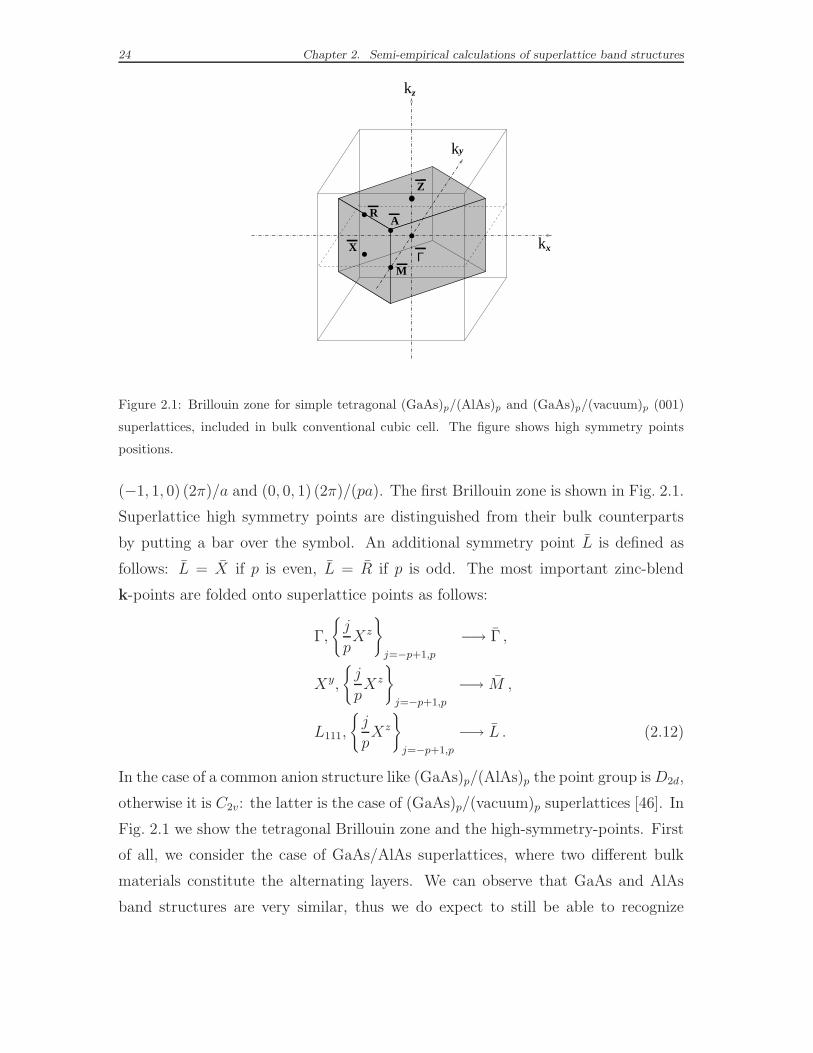
The first step to study the superlattice band structures by the LCBB method is the
calculation of the bulk energy levels and eigenfunctions all over the Brillouin zone.
The dispersions of the energy levels along the high symmetry directions in the fcc
Brillouin zone, for GaAs and AlAs crystals, are shown respectively in Figs. 2.2 and
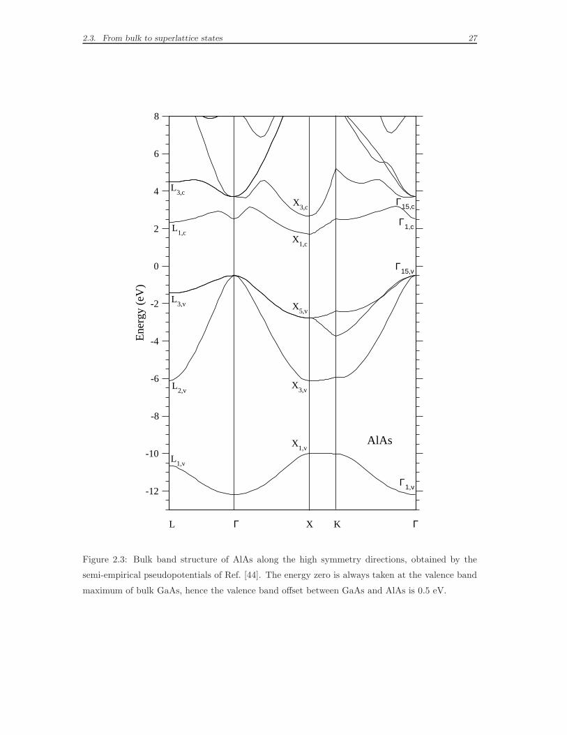
2.3. The energy zero is fixed at the top of the valence band of GaAs, for both GaAs
and AlAs band structures. This choice is meant to emphasize the advantages offered
by the semi-empirical pseudopotentials parametrized in Ref. [44]: the electronic
energies extracted by the diagonalization of the Hamiltonian (2.5) lie on an absolute
energy scale, thus the energy levels of GaAs and AlAs can be directly compared
and the difference between the highest occupied levels of the two materials at Γ
gives the 0.5 eV valence band offset without further adjustments. The fit of s-like
conduction-band edges at the high symmetry points Γ, X, L is excellent, especially
in the case of GaAs. Yet, we will notice that the error remains relevant, even 0.7
eV with respect to the experiment for the p-like GaAs Γ15c (see Tables 3.2 and
3.3). The numeric values of the energy levels at the high symmetry points will be
further discussed in the comparative tables mentioned above, after the presentation
of the analogous ab initio band structure calculations in Section 3.5. It is worth
remembering that the semi-empirical pseudopotential implemented here is local,
whereas the norm-conserving pseudopotential accounts for non-local contributions.
Hence it is expected that the quality of first principle band structure is higher.
Starting from a bulk basis set to expand the superlattice wavefunctions obliges
to think about the way in which the bulk states couple to evolve to the superlattice
states. The cubic symmetry of the bulk lattices is reduced when the superlattice is
built and the growth direction z is no longer equivalent to the orthogonal in-plane
directions x and y. The ideal structure for a lattice-matched system with abrupt
interfaces is a simple tetragonal Bravais lattice, with a supercell defined by the basis
vectors (1, 1, 0)a/2, (−1, 1, 0) a/2, (0, 0, 1) pa, where a is the bulk lattice constant.
The reciprocal lattice is also simple tetragonal, with basis vectors (1, 1, 0) (2π)/a,
24 Chapter 2. Semi-empirical calculations of superlattice band structures
X
.
... -
k
kx
ky
z
M
-
. .RA
--
Z
-
--
---
Γ
-
-
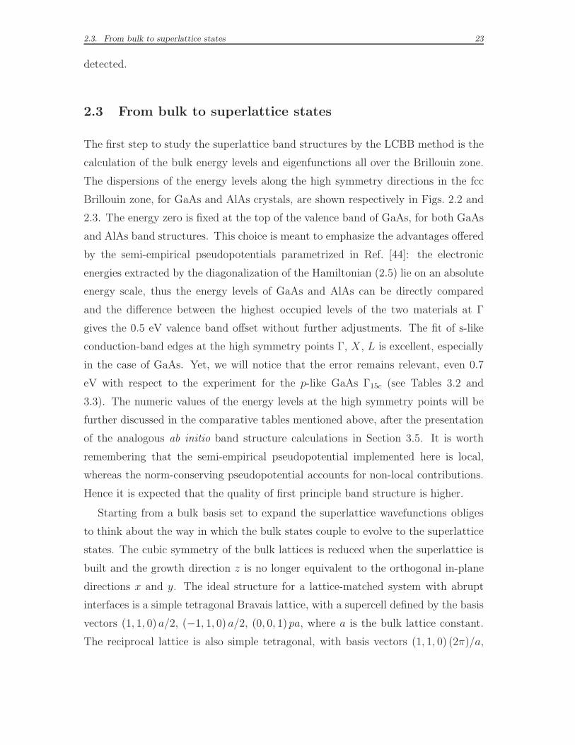
Figure 2.1: Brillouin zone for simple tetragonal (GaAs)p/(AlAs)p and (GaAs)p/(vacuum)p (001)
superlattices, included in bulk conventional cubic cell. The figure shows high symmetry points
positions.
(−1, 1, 0) (2π)/a and (0, 0, 1) (2π)/(pa). The first Brillouin zone is shown in Fig. 2.1.
Superlattice high symmetry points are distinguished from their bulk counterparts
by putting a bar over the symbol. An additional symmetry point L is defined as
follows: L = X if p is even, L = R if p is odd. The most important zinc-blend
k-points are folded onto superlattice points as follows:
Γ,
j
pXz
j=−p+1,p
−→ Γ ,
Xy,
j
pXz
j=−p+1,p
−→ M ,
L111,
j
pXz
j=−p+1,p
−→ L . (2.12)
In the case of a common anion structure like (GaAs)p/(AlAs)p the point group isD2d,
otherwise it is C2v: the latter is the case of (GaAs)p/(vacuum)p superlattices [46]. In
Fig. 2.1 we show the tetragonal Brillouin zone and the high-symmetry-points. First
of all, we consider the case of GaAs/AlAs superlattices, where two different bulk
materials constitute the alternating layers. We can observe that GaAs and AlAs
band structures are very similar, thus we do expect to still be able to recognize
2.3. From bulk to superlattice states 25
-12
-10
-8
-6
-4
-2
0
2
4
6
8
Ene
rgy
(eV
)
L Γ X K Γ
GaAs
Γ1,c
Γ15,v
Γ15,c
Γ1,v
X1,c
X3,c
X5,v
X3,v
X1,v
L1,v
L2,v
L3,v
L1,c
L3,c
Figure 2.2: Bulk band structure of a GaAs crystal along the high symmetry directions, obtained
by the semi-empirical pseudopotentials of Ref. [44]. The energy zero is taken at the valence band
maximum of bulk GaAs.
26 Chapter 2. Semi-empirical calculations of superlattice band structures
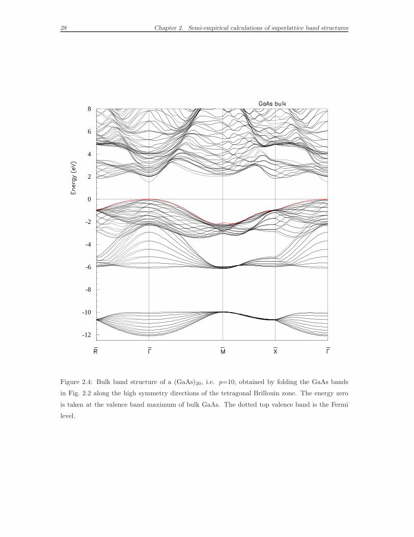
in the superlattice band dispersion the characteristic features present in the bulk
dispersions. However, comparing directly the GaAs/AlAs band dispersion, shown
e.g. in Fig. 2.6, with the bulk band structures in Figs. 2.2 and 2.3 is misleading
and cannot reveal these expected similarities. Before being instructively compared,
the two band structure must be referred to the same Brillouin zone. The tetragonal
supercell contains 2p bulk fcc Wigner-Seitz cells, as a consequence, in the reciprocal
space the tetragonal Brillouin zone is contained in the bulk octahedron Brillouin
zone (see Fig. 2.1). The bulk states outside the superlattice tetragonal Brillouin
zone can be folded into it, by adding tetragonal reciprocal lattice vectors. The
result is a 2p times denser band dispersion along the tetragonal symmetry direc-
tions. The (GaAs)2p band structure showed, for p=10, in Fig. 2.4 is completely
equivalent to the more usual picture in Fig. 2.2. We remember that in the bulk fcc
crystal the directions [001] and [100] are equivalent, hence the bulk band dispersion
is the same along the Γ-M and Γ- Z lines. Now, if we compare the (GaAs)20 band
structure in the tetragonal Brillouin zone with the (GaAs)10/(AlAs)10 superlattice
band structure in Fig. 2.6, we are struck by their similarity. However, they are not
equal, because beside the consequences of folding, also coupling effects occur when
a superlattice is built. Starting from a simple perturbation picture, when the super-
lattice potential is switched on, it couples the previously independent bulk bands,
relative to the same superlattice point q, but coming from non-equivalent points
q+GSL in the bigger fcc Brillouin zone. The effect is an overall modification of the
energy levels. In particular, since the superlattice potential has a lower symmetry,
it can remove level degeneracies. It is time to observe that there are some slight,
but relevant, differences in the bulk band structures of GaAs and AlAs: they differ
with regard to the first conduction band. The conduction minimum of GaAs is in
Γ, the minimum of AlAs is in X instead. Thanks to the absolute energy scale, we
can compare directly the distance in energy of the two edges, which measures only
0.2 eV. Moreover, we know that the bulk k-points Γ and X can be connected by
a superlattice reciprocal lattice vector GSL. Starting again from the perturbation
theory picture, we can easily see that the bulk GaAs eigenfunctions in Γ can be
strongly coupled to the AlAs eigenfunctions in X. This effect is known in literature
as Γ-X coupling and has remarkable consequences on the properties of the minimum
2.3. From bulk to superlattice states 27
-12
-10
-8
-6
-4
-2
0
2
4
6
8
Ene
rgy
(eV
)
L Γ X K Γ
AlAs
Γ1,c
Γ15,v
Γ15,c
Γ1,v
X1,c
X3,c
X5,v
X3,v
X1,v
L1,v
L2,v
L3,v
L1,c
L3,c
Figure 2.3: Bulk band structure of AlAs along the high symmetry directions, obtained by the
semi-empirical pseudopotentials of Ref. [44]. The energy zero is always taken at the valence band
maximum of bulk GaAs, hence the valence band offset between GaAs and AlAs is 0.5 eV.
28 Chapter 2. Semi-empirical calculations of superlattice band structures
-12
-10
-8
-6
-4
-2
0
2
4
6
8
Figure 2.4: Bulk band structure of a (GaAs)20, i.e. p=10, obtained by folding the GaAs bands
in Fig. 2.2 along the high symmetry directions of the tetragonal Brillouin zone. The energy zero
is taken at the valence band maximum of bulk GaAs. The dotted top valence band is the Fermi
level.
2.3. From bulk to superlattice states 29
conduction state in Γ at different superlattice sizes [45, 47, 48]. The coupling be-
tween Γ(Γ1c) and Γ(X1c,3c) states, i.e. the lowest superlattice conduction states at
Γ, which come respectively from Γ and X band-edge states of the constituent bulk
materials (see the state labels in Figs. 2.2 and 2.3), leads to a reciprocal repulsion
between these two levels. Since all zinc-blend X states lie higher in energy than the
GaAs Γ conduction minimum, this symmetry coupling pushes down the Γ(Γ1c) state,
contrasting the upward shift due to confinement. This competition between poten-
tial symmetry and kinetic energy effects results in a non-monotonic Γ (Γ1c) /Γ (X1c)
splitting for small p. For large periods, symmetry induced repulsions rapidly attenu-
ate, as the weight function Wα becomes smaller, and confinement effects dominate,
even though they also decrease as the well width grows. All this determines the
transition form a pseudo-direct (i.e. Γ (X1c) is the conduction minimum) to a direct
(i.e. Γ (Γ1c) is the conduction minimum) gap at a superlattice period p = 11 ± 1
[49].
We have also determined (see the table in Fig. 2.5) the electron effective masses
m∗ from the definition:
E(k) − E0 =h2 |k − k0|2
2m∗ , (2.13)
where E0 is the energy of the band extreme at k0 and k must not be too far from
k0, in order to validate the parabolic approximation. The quality of the obtained
effective masses is particularly important, in view of describing correctly another
important effect, besides the mixing effects: the carrier confinement. We give in
Fig. 2.5 a schematic image of the confinement of an electron in a multilayered struc-
ture. We consider an electron in a conduction band (but the same considerations
are valid for a hole in a valence band) in a GaAs/AlAs superlattice, lying in a state
which comes from a bulk band edge state: it can be represented by a particle of
mass m∗ which feels a rectangular potential, given by the level alignment of the bulk
energy bands along the growth direction z (see the schematic picture in Fig. 2.5).
This corresponds to nothing more than the simple quantum mechanic exercise of a
particle in a periodic repetition of boxes. The AlAs layers act as barriers for the
carriers (both electrons in conduction band and holes in valence band), confined in
the wells made of GaAs. The result is a shift of both the valence and the conduction
energy levels, which makes the gap wider. The effective mass values are related to
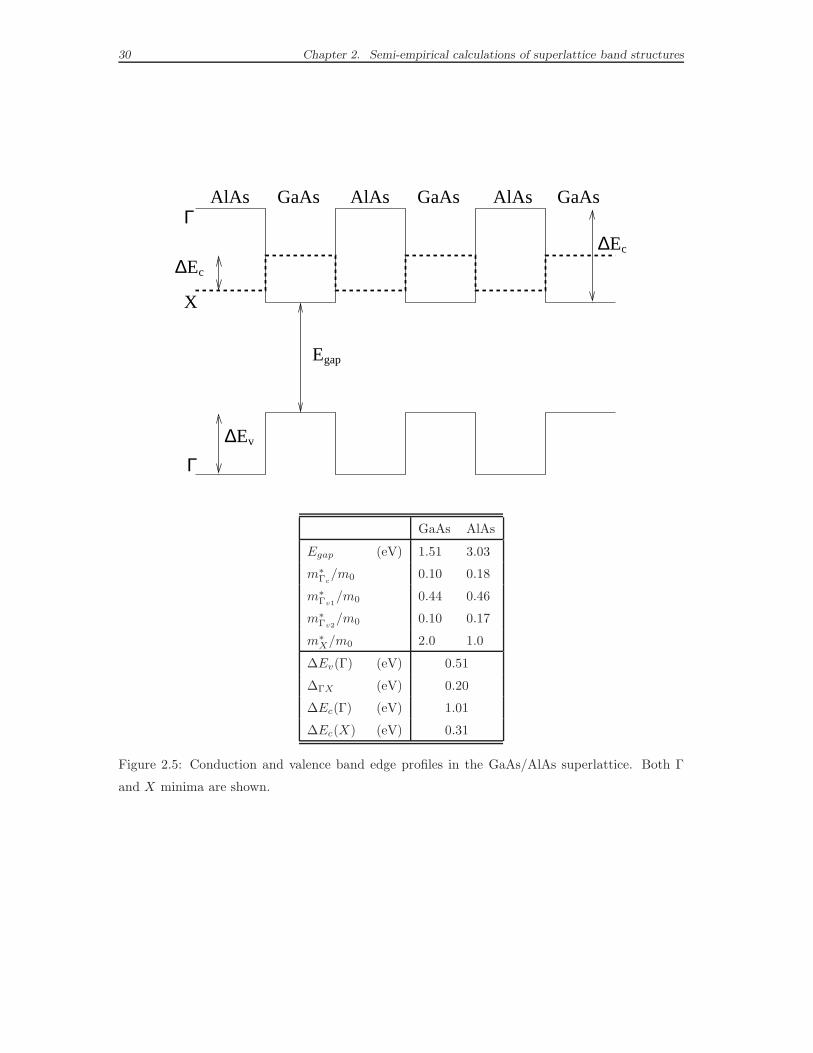
30 Chapter 2. Semi-empirical calculations of superlattice band structures
GaAs GaAs GaAsAlAs AlAsAlAsΓ
v
X
Γ
∆∆
∆
E
E
E
E
gap
c
c
GaAs AlAs
Egap (eV) 1.51 3.03
m∗Γc
/m0 0.10 0.18
m∗Γv1
/m0 0.44 0.46
m∗Γv2
/m0 0.10 0.17
m∗X/m0 2.0 1.0
∆Ev(Γ) (eV) 0.51
∆ΓX (eV) 0.20
∆Ec(Γ) (eV) 1.01
∆Ec(X) (eV) 0.31
Figure 2.5: Conduction and valence band edge profiles in the GaAs/AlAs superlattice. Both Γ
and X minima are shown.
2.4. Calculated superlattice electronic levels 31
the curvature of the bands: the semi-empirical pseudopotentials give satisfactory
effective masses if compared to experiments, as discussed in Ref. [44].
Concerning GaAs/vacuum superlattices, the same considerations are valid, ex-
cept for the fact that there are no AlAs states and thus only GaAs states can mix
with each other. For the vacuum barriers are ideally infinite in height, confinement
effects are significantly stronger and, accordingly, the band gaps are wider than in
GaAs/AlAs systems. If we now compare the GaAs band structure in the tetragonal
Brillouin zone with the GaAs/vacuum superlattice band structure in Fig. 2.7, they
still show similar dispersions. However, as the GaAs/vacuum superlattice has only
half the number of electrons if compared to the bulk GaAs, also the superlattice
band structure has only half the number of bulk bands.
2.4 Calculated superlattice electronic levels
Finally, we show the results of the application of the method LCBB to the single-
particle band structures of (001) (GaAs)p/(AlAs)p and (GaAs)p/(vacuum)p super-
lattices. In practice, the period d = pa has been varied from 4a to 20a. We do not
consider smaller supercells because the superlattice electronic states differ more and
more from bulk states while the layer width decreases, making the expansion on the
bulk states less reliable.
In the case of a GaAs/vacuum superlattice we decide to include the 4 valence
bands and the 4 lowest conduction bands in the basis set. In the case of a GaAs/AlAs
superlattice the roughest selection is to take both GaAs and AlAs bulk states at each
mixed k and n, orthonormalizing at the end the basis set obtained. As GaAs and
AlAs band structures are very similar except for the lowest conduction band (see
again Figs. 2.2 and 2.3 and details of calculation below), we have verified that it is
enough to include only GaAs states for n from 1 to 8 together with the 5th band of
AlAs (i.e. the lowest conduction band). The resulting set must be orthonormalized.
It can easily be seen that the final dimension of the basis is always small (40× 9 for
the largest supercell). When a sufficiently large number of bulk states is used as a
basis set for the LCBB method, the results must converge to those obtained with
a direct diagonalization of the Hamiltonian for the corresponding number of plane
32 Chapter 2. Semi-empirical calculations of superlattice band structures
waves. A comparison of LCBB results with the conventional supercell approach was
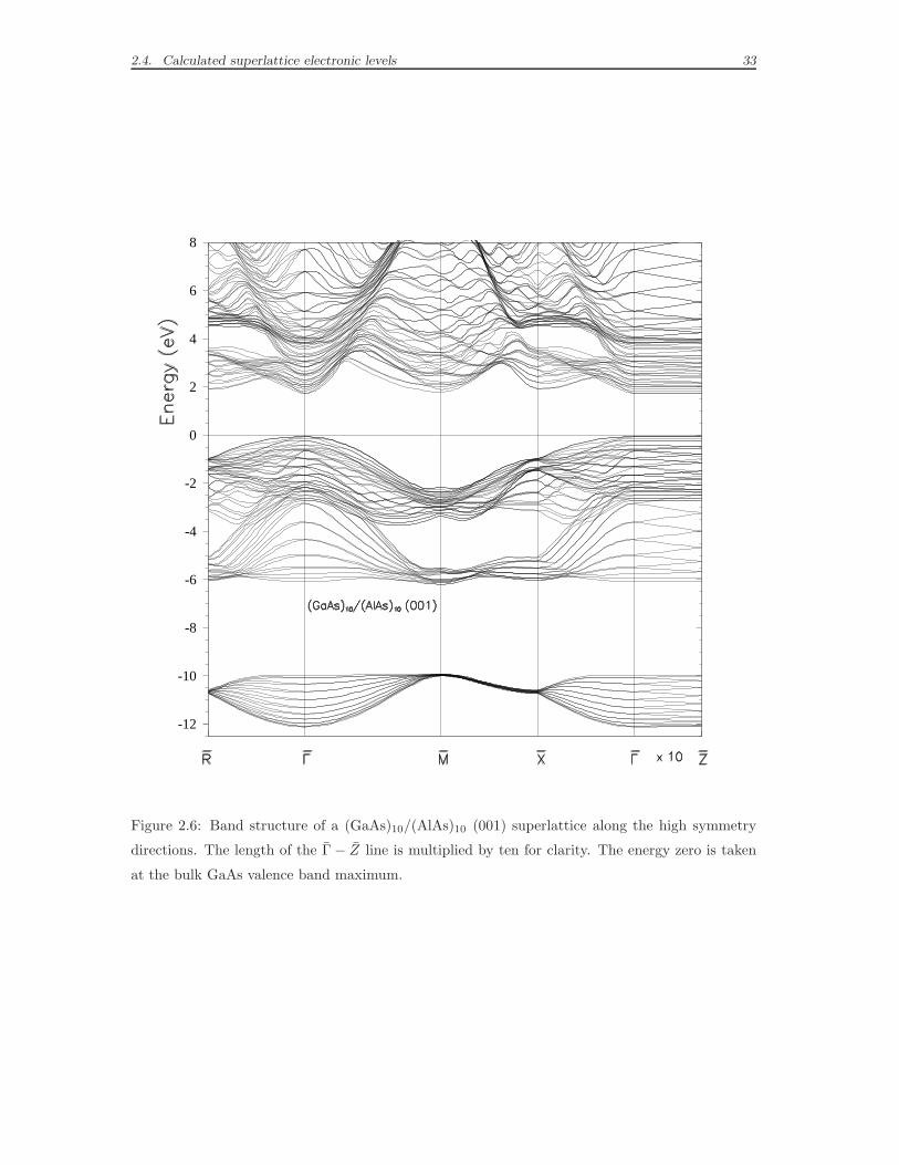
presented in Ref. [29]. Here we have performed a convergence test, which consists
in calculating the energy levels with four different bulk basis sets of increasing size.
Selected results are shown in Tab. 2.1 for (GaAs)10/(AlAs)10 and (GaAs)6/(AlAs)6
superlattices. As far as valence states are concerned, dependence of the energy levels
on the basis set is below 10−3 eV; for the lowest conduction levels the dependence
on the basis set is generally below 0.05 eV, and falls below 10−2 eV when the 5th
band of AlAs is included in the basis. The results of Tab.2.1 justify the use of basis
3), namely n = 1 to 8 for GaAs and n = 5 for AlAs.
Table 2.1: Comparison of energy levels (in eV) at the symmetry points for (GaAs)n/(AlAs)n
superlattices with period n = 6 and n = 10. We show highest valence levels and lowest conduction
levels: the energy zero is taken at the valence band maximum. Four different choices are considered
for the basis set: 1) five GaAs bands for n from 1 to 5, no AlAs bands; 2) eight GaAs bands for n
from 1 to 8, no AlAs bands; 3) eight GaAs bands for n from 1 to 8, the 5th band of AlAs; 4) eight
GaAs bands for n from 1 to 8, four AlAs bands for n from 5 to 8.
basis valence band maximum conduction band minimum
Γ Z R M X Γ Z R M X
n=10
1) 0.0000 -0.0004 -0.8992 -2.1127 -0.8992 1.8318 1.8303 2.0069 1.9048 2.0063
2) 0.0000 -0.0004 -0.8990 -2.1129 -0.8990 1.8173 1.8190 2.0057 1.9014 2.0049
3) 0.0000 -0.0004 -0.8990 -2.1131 -0.8990 1.7949 1.8008 1.9911 1.8588 1.9881
4) 0.0000 -0.0003 -0.8985 -2.1130 -0.8985 1.7884 1.7957 1.9904 1.8590 1.9874
n=6
1) 0.0000 -0.0118 -0.8488 -2.0968 -0.8489 1.9766 1.9940 2.1730 1.9961 2.1561
2) 0.0000 -0.0115 -0.8481 -2.0970 -0.8482 1.9526 1.9567 2.1694 1.9940 2.1535
3) 0.0000 -0.0115 -0.8481 -2.0973 -0.8482 1.9062 1.9109 2.1451 1.9618 2.1053
4) 0.0000 -0.0113 -0.8468 -2.0967 -0.8468 1.9042 1.9098 2.1440 1.9626 2.1043
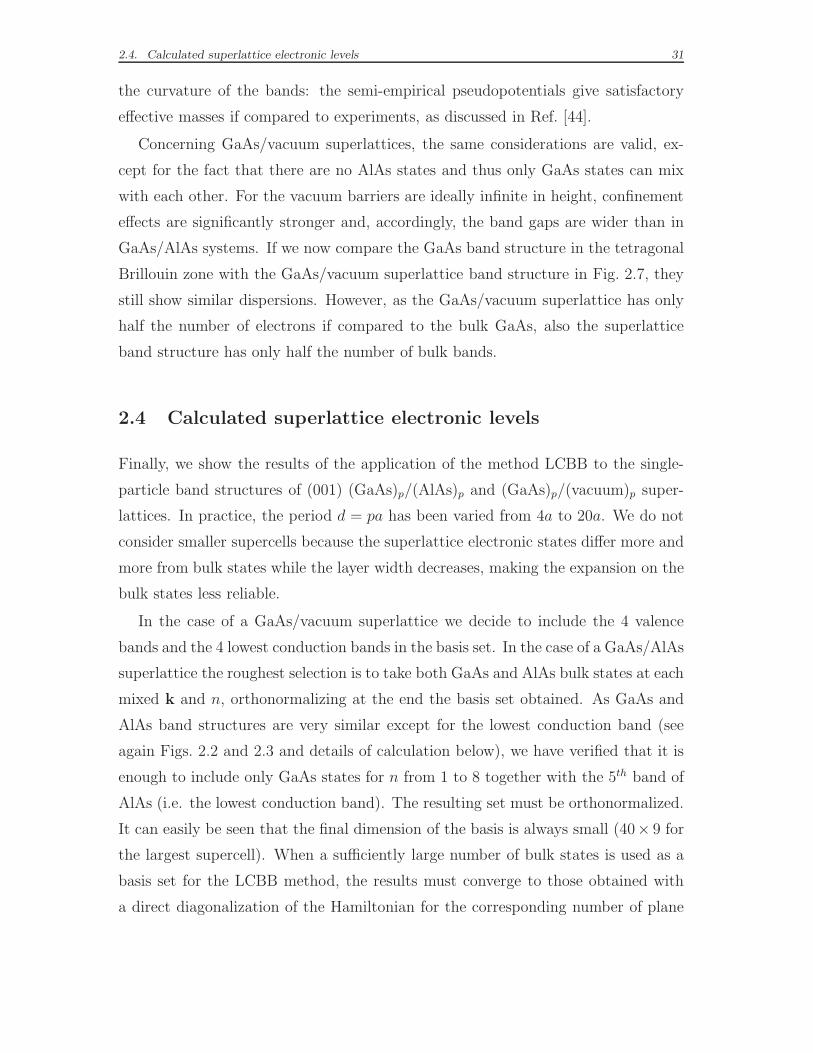
In Figs. 2.6 and 2.7 we show the superlattice energy bands for p=10: the elec-
tron energy levels are plotted along the highest symmetry lines in the tetragonal
Brillouin zone. All trends in the superlattice states obtained by LCBB method were
shown to be reproduced [29], with a surprising accuracy (10-20 meV) and a small
2.4. Calculated superlattice electronic levels 33
-12
-10
-8
-6
-4
-2
0
2
4
6
8
Figure 2.6: Band structure of a (GaAs)10/(AlAs)10 (001) superlattice along the high symmetry
directions. The length of the Γ − Z line is multiplied by ten for clarity. The energy zero is taken
at the bulk GaAs valence band maximum.
34 Chapter 2. Semi-empirical calculations of superlattice band structures
computational effort, down to thin superlattices and up to large periods. Since 2p
k-points in the fcc Brillouin zone are always folded onto the same point q in the
smaller tetragonal Brillouin zone, the number of occupied superlattice bands is 2p
times the number of bulk bands for GaAs/AlAs, p times the number of bulk bands
for GaAs/vacuum superlattices. The dispersion along the direction Γ-M is similar
to the dispersion along the direction Γ-X in the bulk, while the other two directions
Γ-R and Γ-X have no counterpart in the band structures of Figs. 2.2 and 2.3. In
GaAs/AlAs, the dispersion along the growth direction Γ-Z is much smaller than in
the other directions, as expected for superlattice minibands; in GaAs/vacuum the
bands along Γ-Z are flat as tunneling through the vacuum has a negligible effect.
We have discussed how the main differences in the superlattice band structures
compared to the bulk (compare again to Fig. 2.4) can be interpreted in terms of
zone folding and quantum confinement effects; it is also interesting to compare the
band structures of the two superlattices. The superlattice gaps are larger than the
bulk gaps: in particular the GaAs/vacuum gaps are larger than the GaAs/AlAs
ones, as a result of a stronger confinement; moreover the superlattice band gap
widths increase as the superlattice period decreases. The lowering in the crystal
symmetry is responsible for the removal of level degeneracies: as an example in the
GaAs/AlAs D2d superlattice the threefold degenerate valence states at Γ (spin-orbit
is neglected) are split in a twofold-degenerate and a non-degenerate state, while in
the GaAs/vacuum C2v superlattices the degeneracy is completely removed.
In GaAs/vacuum bands we clearly see the appearance of states lying in the for-
bidden energy gaps. The lowest one lies in the gap from -10 to -6 eV, while two other
ones lie in the optical gap from 0 to about 2 eV. A fourth state can be recognized at
-5 eV around the point M , while in other regions of the Brillouin zone it resonates
with the energy bands. Indeed, four surface states or resonances are expected from
the presence of two dangling bonds at the two interfaces of each GaAs layers. We
can identify the surface states by studying the behavior of the probability |ψ|2 to
find an electron along the growth direction z, averaged over the in-plane x, y co-
ordinates. Taking as an example the conduction miniband states at Γ, where the
potential profile is characterized by 0.5 eV deep wells in GaAs layers, we observe
(see Fig. 2.8) that an electron in a surface state (j = 39 in the exemplified case)

2.4. Calculated superlattice electronic levels 35
-12
-10
-8
-6
-4
-2
0
2
4
6
8
Figure 2.7: Band structure of a (GaAs)10/ (vacuum)10 (001) superlattice along the high symmetry
directions. The energy zero is taken at the bulk GaAs valence band maximum. The uppermost
occupied band is number 40 (dotted).
36 Chapter 2. Semi-empirical calculations of superlattice band structures
0
0.1
0.2
0.3
0.4
0.5
0.6
0.7
0.8
0.9
1
0
0.1
0.2
0.3
0.4
0.5
0.6
0.7
0.8
0.9
1
-10 -8 -6 -4 -2 0 2 4 6 8 10
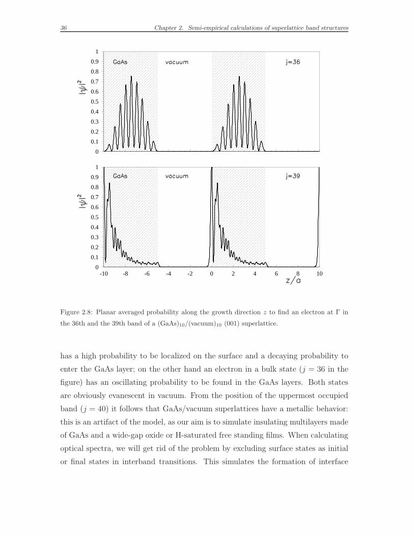
Figure 2.8: Planar averaged probability along the growth direction z to find an electron at Γ in
the 36th and the 39th band of a (GaAs)10/(vacuum)10 (001) superlattice.
has a high probability to be localized on the surface and a decaying probability to
enter the GaAs layer; on the other hand an electron in a bulk state (j = 36 in the
figure) has an oscillating probability to be found in the GaAs layers. Both states
are obviously evanescent in vacuum. From the position of the uppermost occupied
band (j = 40) it follows that GaAs/vacuum superlattices have a metallic behavior:
this is an artifact of the model, as our aim is to simulate insulating multilayers made
of GaAs and a wide-gap oxide or H-saturated free standing films. When calculating
optical spectra, we will get rid of the problem by excluding surface states as initial
or final states in interband transitions. This simulates the formation of interface

2.4. Calculated superlattice electronic levels 37
states or defects in a GaAs/oxide superlattice, which would saturate the dangling
bonds. The surface resonance cannot be easily eliminated, but it produces small
effects on the spectra, since it lies deep in the valence band.
In this chapter we have discussed the LCBB approach to study the superlattice
band structures. This approach, which expands the electronic states of the super-
lattice on the basis of bulk states, calculated by semi-empirical pseudopotentials, is
found to be adequate and practical for superlattices characterized by medium to in-
termediate periods. It has revealed to be particularly suitable for calculating how the
band structures of the bulk materials are modified when an artificial confining po-
tential is applied. We have written a computational code to calculate the electronic
states in superlattices. We have applied the code to study the evolution of a bulk
state into a superlattice state, gaining a clear insight on the role played by the con-
finement, the bulk states-coupling and the reduction of the symmetry, all involved in
the formation of a superlattice. The superlattice gaps result larger: in particular the
GaAs/vacuum gaps are larger than the GaAs/AlAs ones. Moreover, the superlattice
gaps become larger when the confinement increases, as a consequence of the size re-
duction. The lowering in the crystal symmetry and the mixing of bulk states induce
a modification of the energy levels and remove level degeneracies.

38 Chapter 2. Semi-empirical calculations of superlattice band structures
Chapter 3
Ab-initio calculations of
superlattice band structures
In this chapter we present our second choice for band structure calculations of bulk
and nanostructure semiconductor systems. We move from the semi-empirical ap-
proach to a well-known first principle theory: the Density Functional Theory (DFT).
If compared to the LCBB method presented in the previous chapter, the first strik-
ing difference in the ab initio DFT approach is the total absence of experimental
inputs. Within a pseudopotential approach, starting from the mere knowledge of the
atomic numbers, atomic pseudopotentials can be fitted to calculations for the iso-
lated atoms. Next, an hypothesis on the geometric structure of the system is all we
need to build up the Hamiltonian operator. The most stable structure can be found
among all the different hypothesized structures, by searching for the minimum of the
calculated total energy. It is evident that the development of ab initio techniques has
given a much stronger predictive character to the theory of electronic properties in
the matter. Details on the procedure we have followed to construct norm-conserving
ab initio pseudopotentials can be found in Appendix B. In the following sections,
at first, we will present the fundamentals of the Density Functional Theory. They
are intended to be a practical guide to accompany the immediately successive ex-
position of our results, namely the electronic ground state properties and the band
structures of bulk (i.e. GaAs and AlAs) and superlattice (i.e. GaAs/AlAs) systems.
We have analyzed the structural properties and the electronic band structures of
39

40 Chapter 3. Ab-initio calculations of superlattice band structures
GaAs and AlAs crystals. Results in agreement with both the experiment and anal-
ogous calculations existing in literature are a reassuring proof about the quality of
the norm-conserving pseudopotentials we have built. In addition, a good bulk band
dispersion is promising concerning the quality of further calculations of the optical
response. However, we are essentially interested in (GaAs)p/(AlAs)p superlattices.
For superlattices with a very short period, the expansion over bulk states becomes
unreliable (unless using a very large basis) and LCBB calculations have not been
pushed to periods p smaller than 4. Some results for the band structure of small to
medium size (1 ≤ p ≤ 8) systems will be presented in the last section. Analogous ab
initio calculations are available in literature only for the smallest periods p. Thus,
we will focus on the comparison of the DFT band structure for the superlattice
period p=8 to the corresponding semi-empirical band structure.
We will adopt atomic units, as it is usually done in literature: h = e2 = me = 1.
The spin and space coordinates are abbreviated by x ≡ (r, σ).
3.1 Density Functional Theory
The Density Functional Theory (DFT), in the Kohn-Sham formalism, provides a
powerful computational scheme, which allows to determine exactly the ground-state
properties even of complex systems of interacting particles, simply solving a single-
particle-like equation. Let us consider a system made of N fermions (let us say elec-
trons), interacting with each other via the Coulomb potential v (ri, rj) = 1/ |ri − rj|.The system experiences an external potential w(r), which is supposed at the mo-
ment to be time-independent. In the specific case of electrons in an infinite periodic
solid, this external potential is due to the Coulomb interaction between electrons
and ion cores, fixed on the lattice sites. The Hamiltonian operator
H = T +W + V
=N∑
i=1
(
−1
2∇2
ri+ w (ri)
)
+1
2
N∑
i6=j
v (ri, rj) (3.1)
is the main ingredient in the time-dependent Schrodinger equation, which determines
the time evolution of the system:
H (x1,x2, . . . ,xN) Ψ (x1,x2, . . . ,xN , t) = i∂Ψ (x1,x2, . . . ,xN , t)
∂t. (3.2)
3.1. Density Functional Theory 41
The stationary states are the eigenstates of the time-independent Schrodinger equa-
tion:
H (x1,x2, . . . ,xN )ψ (x1,x2, . . . ,xN) = Eψ (x1,x2, . . . ,xN) . (3.3)
An analytical solution of the Eq. (3.3) is not feasible, except for some extremely
simple model systems. Among the variety of possible approaches to tackle the
problem, Thomas and Fermi [50, 51] were the first to designate the charge density
ρ (r), instead of the many-body wavefunction, as the basic quantity to describe
the ground state properties of the system. The advantage is evident: the electron
density,
ρ (r) = N∫
dx2 . . .∫
dxNψ∗ (r,x2, . . . ,xN)ψ (r,x2, . . . ,xN) , (3.4)
is much easier to manage: it reduces the degrees of freedom from 3N to 3 and it is
a measurable physical quantity.
3.1.1 The Hohenberg-Kohn theorem
The formal bases of DFT are the theorems formulated in 1964 by Hohenberg and
Kohn [52]. The original proof is valid for a non-degenerate ground state and a
w-representable particle density, i.e. the ground state density belongs to a system
which undergoes an external local potential w. For the proofs of the theorems
and their generalization (to, e.g., degenerate ground states, bosons, non-adiabatic
systems, magnetic systems, fully relativistic systems, superconducting systems, N -
representation of the particle density, etc. . . .) we suggest to see Ref. [53]. Here we
present the physical contents of the original theorems.
1st HK Theorem: Let us consider a system of N electrons, described by the
Hamiltonian:
H =N∑
i=1
(
−1
2∇2
ri+ w (ri)
)
+1
2
N∑
i6=j
v (ri, rj) . (3.5)
The electrons are thus subjected to an external potential w (r) and the ground
state charge density is ρ0(r). If we substitute the potential w′ (r) for the po-
tential w (r) in 3.5 and we observe that the new electron density ρ′0(r), relative
to the ground state, is equal to ρ0(r), then w (r) and w′ (r) can only differ by
42 Chapter 3. Ab-initio calculations of superlattice band structures
a constant:
w′ (r) = w (r) + const . (3.6)
2nd HK Theorem: Let us define the energy functional of the density E [ρ] in the
form
E [ρ] = 〈N | − 1
2∇2
ri+
1
2
N∑
i6=j
v (ri, rj) |N〉 +∫
w (r) ρ (r) dr
= F [ρ] +∫
w (r) ρ (r) dr , (3.7)
where F is a universal functional of the density. Once the external potential
w (r) has been fixed, the energy functional E [ρ] has its minimum, the ground
state energy E0, at the physical ground state density ρ0 (r):
E0 = E [ρ0] . (3.8)
The first theorem states that there is a bijective relation between the external
potential w (r) (to within a constant) and the ground state density ρ (r): this implies
that the Hamiltonian is completely described by knowing the ground state density,
thus all the ground state properties of the N-electrons system (e.g. the total energy)
are functionals of ρ (r). The Hohenberg-Kohn (HK) theorems have the limited
purpose to prove that a universal functional of the electron density exists, they
do not derive its actual expression. A direct minimization of the functional (3.7)
is usually not applicable, because no good expression for the kinetic energy as a
functional of ρ is known, except for simple metals. The Kohn-Sham (KS) scheme,
a reformulation of the theory based on the KS orbitals instead of the mere density,
is the starting-point of most of the actual calculations.
3.1.2 The Kohn-Sham scheme
The variational scheme proposed by Kohn and Sham [54] is an useful tool to clarify
the physical contents of the theory. Let us consider the system of N interacting
electrons, described by the Hamiltonian (3.1):
H = T +W + V .

3.1. Density Functional Theory 43
We introduce now an auxiliary system composed by N non-interacting particles in
an external potential W ′, described by the one-particle Hamiltonian H ′:
H ′ = T +W ′ . (3.9)
The KS scheme is based on the hypothesis that it exists such a local potential W ′,
that makes the ground state electronic density ρ′(r) of the non-interacting system
equal to the ground state electronic density ρ(r) of the interacting system:
ρ (r) = ρ′ (r) . (3.10)
It is clear that if a non-interacting system with the required characteristics exists,
then, according to the HK theorems, it must be unique. At the moment, we assume
that it is always possible to find such a potential W ′; its existence is formally proved
for w-representable densities (see Ref. [55]) and generalized to N -representable den-
sities (see Ref. [53]). The charge density of the non-interacting system can be ex-
pressed as a sum of single-particle charge densities; this holds also for the real charge
density thanks to the equality (3.10):
ρ (r) = ρ′ (r) =N∑
i=1
|φi (r)|2 . (3.11)
The sum includes the eigenfunctions φi relative to the N lower eigenvalues, coming
from the solution of the Schrodinger equation for the non-interacting system:[
−1
2∇2
ri+ w′ (r)
]
φi (r) = ǫiφi (r) . (3.12)
The HK functional associated to the auxiliary system is:
E ′ [ρ] = T ′ [ρ] +∫
w′ (r) ρ (r) dr , (3.13)
where also the kinetic energy of the non-interacting electrons T ′ [ρ] is a functional
of the density ρ(r) , as a consequence of the fact that the eigenfunctions φi are
functionals of the density:
T ′ [ρ] =N∑
i=1
∫
φ∗i (r)
[
−1
2∇2
ri
]
φi (r) dr . (3.14)
We can now rewrite the HK functional for the real system in a more profitable way:
E [ρ] = T ′ [ρ] +1
2
∫
dr∫
dr′ρ (r) ρ (r′) v (r, r′) +∫
w (r) ρ (r) dr + Exc [ρ] . (3.15)

44 Chapter 3. Ab-initio calculations of superlattice band structures
The kinetic energy T ′ [ρ] is now the kinetic energy of a non-interacting electron gas
and the second term gives the Coulomb energy due to the classic interaction of an
electron gas of density ρ(r). By comparing the expression (3.7) and (3.15), we get
a definition for the functional Exc, which accounts for the many-body exchange and
correlation effects among electrons:
Exc [ρ] = F [ρ] − 1
2
∫
dr∫
dr′ρ (r) ρ (r′) v (r, r′) − T ′ [ρ] . (3.16)
The form of the still unknown external potential W ′ can be fixed minimizing the
energy functional E [ρ] in (3.15), by imposing that his first variation vanishes:
δE [ρ] = 0 . (3.17)
It results that the searched potential for the non-interacting system is a function
of the real external potential, the Coulomb potential and the so called exchange-
correlation (xc) potential:
w′ (r) = w (r) +∫
dr′ρ (r′) v (r, r′) + vxc ([ρ], r) , (3.18)
where the xc potential is defined as
vxc ([ρ], r) =δExc [ρ]
δρ (r). (3.19)
If we now introduce the potential w′ from Eq. (3.18) into the Schrodinger equation
(3.12), we obtain the Kohn and Sham equations:
heffKS φi =
[
−1
2∇2 + w′
]
φi = ǫi φi . (3.20)
The KS equations (3.20) and the expression of w′(r) (3.18) have both a functional
dependence on ρ(r), which imposes a simultaneous self-consistent solution. The
exchange-correlation term is a functional of the density, local in space, which makes
the resolution of the equations easier than the solution of e.g. analogous Hartree-
Fock equations. Looking at the form of the one-body potential w′(r), we can see
that the external ionic attractive potential w is modified by the screening due to the
interaction between charges: this suggests to interpret it as the effective potential
felt by one electron in the mean field created by the other electrons. Thanks to
its construction, the effective potential w′(r) of the non-interacting system gives the
3.1. Density Functional Theory 45
correct density ρ(r) of the interacting system. This quantity, together with the total
energy of the electron system, has a real physical meaning within the KS scheme.
The solutions of the KS equations, i.e. the one-particle wavefunctions φi and the
eigenvalues ǫi, are instead, strictly speaking, nothing more than the eigenstates
and energy levels of the non-interacting system. We remark that the HK theorems
concern only the ground state properties of stationary systems: it is not correct to
extract from the DFT, at least without further formal justifications, any information
about the excited states or about time-dependent transitions. Nevertheless, we will
see that the theory has proved to be a good basis for a perturbation approach and
for time-dependent extensions, aiming at treating this kind of problems.
This scheme allows in principle the exact determination of the ground state en-
ergy. In practice, it is inevitable to make an approximation for the xc potential.
The exchange-correlation functional is a universal functional, in the sense that once
it is known for a model system, it can be simply transferred to all the others sys-
tems with the same internal interaction potential, whatever the external field is.
Unfortunately, there are no solved models for arbitrary densities ρ (r). The only
available solution is the extremely accurate calculation for the electron jellium at
the constant density ρ (r) = ρ0 [56, 57, 58]. Being the exchange-correlation energy
Exc in general unknown, the possibility to describe physical systems relies on the
effective substitution of a simple and realistic approximation for this functional.
3.1.3 The Local Density Approximation
The Local Density Approximation (LDA) consists in expressing the functional de-
pendence of the exchange-correlation energy on the density with a simple dependence
on the local value of the density. It is defined by:
ELDAxc [ρ] =
∫
ρ (r) ǫxc (ρ (r)) dr , (3.21)
where ǫxc is the exchange-correlation energy for a particle in an interacting ho-
mogeneous electron gas, which is known with a very satisfactory precision from
many-body Monte Carlo numerical simulations [56, 57, 58]. The correlation energy
occurring in our calculations has been parametrized as follows [57]:
ǫhomxc [ρ (r)] = γ/ (1 + β1
√rs + β2rs) , (3.22)
46 Chapter 3. Ab-initio calculations of superlattice band structures
for rs ≥ 1, where
ρ (r) =(
4
3πr3
s
)−1
, (3.23)
and
γ = −0.14230 , β1 = 1.05290 , β2 = 0.3334 . (3.24)
Since the LDA is exact in case of homogeneous systems, it has been thought to be
suitable to describe those physical systems where the charge density varies slowly,
like metals. This is a strong restriction, but the approximation has surprisingly
turned out to be valid in a vaster range of circumstances, like in semiconductors.
Such an unexpected success is due to the fact that the LDA, even in case of strongly
inhomogeneous systems, satisfies exactly some sum rules which must hold for the real
pair correlation function of the system. In general, quantities derived by comparing
total energies, like ground state geometries, phonon frequencies, and moments of
the density are well reproduced [59] within this simple approximation. These topics
will be discussed further in Section 3.3. There are some possible generalizations of
the LDA: including a correction dependent on the gradient of the density ρ (r), as
already suggested by Hohenberg and Kohn [52], we get the Gradient Density Approx-
imation (GDA). Some other approaches beyond LDA, like the Generalized Gradient
Approximation (GGA) [60, 61], the Average-Density Approximation (ADA), and
the Weighted Density Approximation (WDA) [62], have been object of increasing
interest in the last years. However exactly satisfied within the LDA, the sum rules
are not satisfied within its generalizations. That’s why an improvement of the LDA
is not as straightforward as it might appear [59]. It is not clear yet if it exists an
alternative non-local scheme which is able to guarantee better results if compared
to the LDA. Up to now the LDA is widely applied in literature. The extension to
spin-polarized systems is called Local Spin-Density Approximation (LSDA). In this
work, however, we will always deal with spin-paired electrons.
3.2. Technical aspects 47
3.2 Technical aspects
3.2.1 Plane wave basis
When studying an infinite system composed by a repeated periodic unit, both a cell
or a supercell, the most natural choice for the expansion of the wavefunctions is the
plane wave representation
eiG·r
G∈RL. In fact, according to the Bloch theorem,
the single electron wavefunction can be expanded as follows:
φn,k (r) =1√Ωeik·r∑
G
cn,k (G) eiG·r , (3.25)
where Ω is the volume of the Wigner-Seitz cell (or of the supercell in case of super-
lattices) and G are the reciprocal lattice vectors. The wave-vectors k, lying inside
the first Brillouin zone, label the electronic states together with the band index n.
The choice of a plane wave basis presents some advantages:
• They simplify the evaluation of derivatives and integrals, making easier to cal-
culate the matrix elements of the Hamiltonian.
• They allow the application of Fast Fourier Transform (FFT) formalism, allow-
ing to move rapidly from the direct to the reciprocal space and vice-versa.
• They form a complete and orthonormal set.
• For open systems with some “vacuum”, like cluster and surfaces or, in a future
perspective, GaAs/vacuum superlattices, it is convenient that the set does not
depend on the atomic positions.
• The truncation of the in principle infinite basis set is given by a cutoff in energy:
1
2|k + G|2 ≤ Ecutoff , (3.26)
which is linked to the number of plane waves NPW in the basis by the relation
NPW ≃ Ω (Ecutoff)3/2 . (3.27)
The achievement of convergence for total energy calculations can be controlled
without ambiguity by increasing the cutoff.
48 Chapter 3. Ab-initio calculations of superlattice band structures
A plane wave basis set is particularly suitable in case of a pseudopotential approach
(see Appendix B). In such a case only the valence wavefunctions, which are less
localized than the core ones, have to be calculated. Localized basis sets, on the
other hand, should be preferred when one is interested in highly localized electronic
states (e.g. core atomic-like states).
In our calculations, the convergence has been achieved working with plane waves
up to a kinetic energy cutoff of 25 Ry for both GaAs and AlAs bulk crystals. Con-
cerning the superlattices GaAs/AlAs, an higher cutoff of 35 Ry is needed to achieve
the same degree of accuracy. We have proved that these sets guarantee an error
within a few meV both for the total energy and for the KS eigenvalues.
3.2.2 Sets of k-points for integration over the Brillouin zone
All sums over the allowed k-points in the Brillouin zone become integrals in the
limit of an infinite periodic crystal. In particular, the central quantity which defines
the system, the charge density,
ρ (r) =1
Nk
occ∑
n
BZ∑
k
|φn,k (r)|2 , (3.28)
is transformed in:
ρ (r) =Ω
(2π)3
∫
BZdk
occ∑
n
|φn,k (r)|2 . (3.29)
To perform a numerical calculation, in practice, the integral must be turned back into
a sum over a set of weighted k-points. If the function to be integrated, as it happens
in expression (3.29), is symmetric in the reciprocal coordinates, these points, called
special points can be chosen exploiting the symmetry properties. The introduction
of the concept of special points is due to Baldereschi [63]. Then, Chadi and Cohen
[64] and, later, Monkhorst and Pack [65] have elaborated his idea. Their methods
are now widely used. In comparison with an arbitrary grid of points, which does
not reflect the symmetries of the Brillouin zone, the special points reduce drastically
the number of points needed to attain a specific precision in calculating integrals.
In the numerical computation of charge densities for bulk fcc GaAs and AlAs
we have performed sums over a grid of 10 special k-points in the irreducible part
of the Brillouin zone. This grid of points has been built following the procedure of
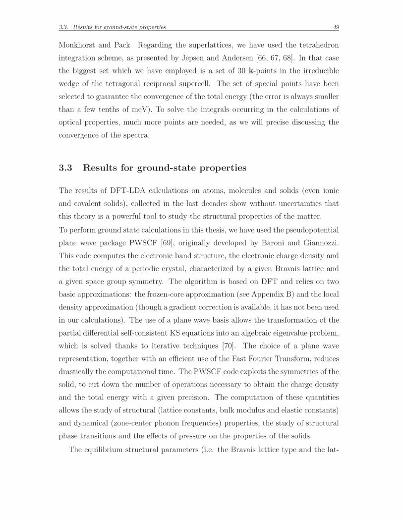
3.3. Results for ground-state properties 49
Monkhorst and Pack. Regarding the superlattices, we have used the tetrahedron
integration scheme, as presented by Jepsen and Andersen [66, 67, 68]. In that case
the biggest set which we have employed is a set of 30 k-points in the irreducible
wedge of the tetragonal reciprocal supercell. The set of special points have been
selected to guarantee the convergence of the total energy (the error is always smaller
than a few tenths of meV). To solve the integrals occurring in the calculations of
optical properties, much more points are needed, as we will precise discussing the
convergence of the spectra.
3.3 Results for ground-state properties
The results of DFT-LDA calculations on atoms, molecules and solids (even ionic
and covalent solids), collected in the last decades show without uncertainties that
this theory is a powerful tool to study the structural properties of the matter.
To perform ground state calculations in this thesis, we have used the pseudopotential
plane wave package PWSCF [69], originally developed by Baroni and Giannozzi.
This code computes the electronic band structure, the electronic charge density and
the total energy of a periodic crystal, characterized by a given Bravais lattice and
a given space group symmetry. The algorithm is based on DFT and relies on two
basic approximations: the frozen-core approximation (see Appendix B) and the local
density approximation (though a gradient correction is available, it has not been used
in our calculations). The use of a plane wave basis allows the transformation of the
partial differential self-consistent KS equations into an algebraic eigenvalue problem,
which is solved thanks to iterative techniques [70]. The choice of a plane wave
representation, together with an efficient use of the Fast Fourier Transform, reduces
drastically the computational time. The PWSCF code exploits the symmetries of the
solid, to cut down the number of operations necessary to obtain the charge density
and the total energy with a given precision. The computation of these quantities
allows the study of structural (lattice constants, bulk modulus and elastic constants)
and dynamical (zone-center phonon frequencies) properties, the study of structural
phase transitions and the effects of pressure on the properties of the solids.
The equilibrium structural parameters (i.e. the Bravais lattice type and the lat-

50 Chapter 3. Ab-initio calculations of superlattice band structures
tice parameters in solids) can be determined ab initio, by inspecting the minimum
of the total energy. In practical applications, the absolute convergence of the total
energy is not very important. The most important quantities are the energy differ-
ences between different states of the solid. Since energy differences converge more
rapidly than the energy itself, it is usually possible to obtain a precision higher than
the total energy error (in our case about a few meV). To illustrate this point, we
have studied two structural properties: the lattice constant a0 and the bulk modulus
B0. These quantities are related to the curvature of the function E(Ω) around the
equilibrium volume Ω0. The theoretical lattice constant has the value a0, which
corresponds to Ω0, while the bulk modulus is related to the curvature of the energy
curve at its minimum:
B0 = −Ω∂2E
∂Ω2
∣
∣
∣
∣
∣
Ω=Ω0
. (3.30)
With respect to our bulk material, it is known that both GaAs and AlAs at zero
pressure have a cubic structure, based on tetrahedral units. Phase diagrams under
pressure have been studied both experimentally and theoretically [71, 72, 73, 74,
75, 76, 77]. We have therefore imposed the zinc-blend structure and minimized the
total energy as a function of the primitive cell volume Ω. Starting from the curves
of the total energy E(Ω) and the pressure P (Ω) due to internal hydrostatic stress
at a non-equilibrium volume, the cohesion energy and the bulk modulus can be
easily determined, interpolating the values E(Ω) or P (Ω) with suitable equations of
state. There are many choices for the interpolating curves. Close to the minimum
the curve is a parabola, but the points deviate rapidly from the quadratic law and,
at a large distance from a0, it is necessary to fit the points to something more
sophisticated. One of the most popular fitting curves is the Murnaghan equation
[78], which depends on three parameters: Ω0, B0, B′0 (the derivative of the bulk
modulus with respect to pressure):
E(Ω) =Ω0B0
B′0
[
1
B′0 − 1
(
Ω0
Ω
)B′
0−1
+Ω
Ω0
]
+ const . (3.31)
Often, it is preferred to adjust the pressure P, via the Birch-Murnaghan [79] equation
of state:
P =3
2B0
(
(
Ω
Ω0
)−7/3
−(
Ω
Ω0
)−5/3)[
1 +3
4(B′
0 − 4)
(
(
Ω
Ω0
)−2/3
− 1
)]
. (3.32)
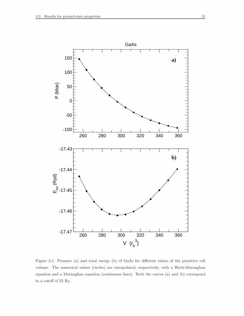
3.3. Results for ground-state properties 51
260 280 300 320 340 360-100
-50
0
50
100
150P
(kb
ar)
GaAs
260 280 300 320 340 360
V (rb3)
-17.47
-17.46
-17.45
-17.44
-17.43
Eto
t (R
yd)
a)
b)
Figure 3.1: Pressure (a) and total energy (b) of GaAs for different values of the primitive cell
volume. The numerical values (circles) are interpolated, respectively, with a Birch-Murnaghan
equation and a Murnaghan equation (continuous lines). Both the curves (a) and (b) correspond
to a cutoff of 25 Ry.

52 Chapter 3. Ab-initio calculations of superlattice band structures
An example of interpolation is illustrate in Fig. 3.1. In Table 3.1 we summarize the
obtained fitting parameters, in comparison with experimental measurements and
analogous results found in literature. When the interpolating function is specified
in the articles, the values in literature has to be compared with quantities we have
obtained by the same equations of state.
We have shown these results, because a comparison with similar ab initio calcu-
lations and experimental values is extremely important to evaluate the reliability
of the norm-conserving pseudopotential that we have generated. Some tests that
can be executed directly on the atom, to assess the quality of the pseudopotentials,
are discussed in Appendix B. Nevertheless, after executing the atomic tests, a final
validation is still needed: the calculation of the structural properties for an infinite
bulk crystal is, certainly, a proving test. An agreement within 1%-3% with the
experiment for the lattice constant and an agreement within 5%-10% for the bulk
modulus indicate that the calculations are reliable. In our case the agreement is
even better. In LDA the errors on the lattice constants are systematic: all the bond
strengths are overestimated [81], thus calculated lattice constants are too small.
At last, before applying calculations to superlattice systems, we have reproduced the
ground state calculations of the bulk GaAs, choosing to describe the cubic structure
in terms of simple tetragonal supercells, like (GaAs)2, (GaAs)4, (GaAs)6, by lower-
ing the symmetry of the fcc cubic point group. It is obvious that two different views
of the same problem must lead to the same results. Thus, the test is intended to
verify that the passage from the cubic symmetry of the bulk to the tetragonal sym-
metry of the superlattice does not introduce an additional font of numerical error
in calculations. This occurrence has been excluded, by checking the convergence of
the k-points set, assuring that the difference in the total energy between the fcc and
the tetragonal description is less than 1 meV.
3.4 Kohn-Sham eigenstates and quasi-particle states
We are now leaving the study of structural properties to focus on the transitions
to excited states. When dealing with an interacting particle system, the easier
one-particle description can be retained at the price to introduce the concept of
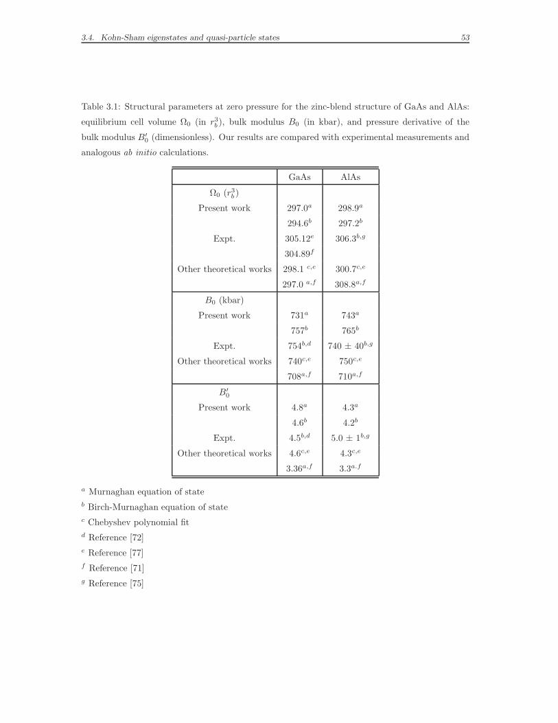
3.4. Kohn-Sham eigenstates and quasi-particle states 53
Table 3.1: Structural parameters at zero pressure for the zinc-blend structure of GaAs and AlAs:
equilibrium cell volume Ω0 (in r3
b ), bulk modulus B0 (in kbar), and pressure derivative of the
bulk modulus B′0 (dimensionless). Our results are compared with experimental measurements and
analogous ab initio calculations.
GaAs AlAs
Ω0 (r3
b )
Present work 297.0a 298.9a
294.6b 297.2b
Expt. 305.12e 306.3b,g
304.89f
Other theoretical works 298.1 c,e 300.7c,e
297.0 a,f 308.8a,f
B0 (kbar)
Present work 731a 743a
757b 765b
Expt. 754b,d 740 ± 40b,g
Other theoretical works 740c,e 750c,e
708a,f 710a,f
B′0
Present work 4.8a 4.3a
4.6b 4.2b
Expt. 4.5b,d 5.0 ± 1b,g
Other theoretical works 4.6c,e 4.3c,e
3.36a,f 3.3a.f
a Murnaghan equation of state
b Birch-Murnaghan equation of state
c Chebyshev polynomial fit
d Reference [72]
e Reference [77]
f Reference [71]
g Reference [75]
54 Chapter 3. Ab-initio calculations of superlattice band structures
quasi-particle (QP) states. A quasi-electron differs from a bare electron because it
moves dressed by the interaction with a cloud of surrounding electrons. The screen-
ing change its effective mass and makes finite its lifetime. The quasi-particle energies
are given by the energies needed to add/subtract an electron to/from the system.
These quasi-particle levels can be measured respectively in inverse-photoemission
or photoemission spectroscopy and can be calculated within a coherent many-body
theory framework. The many-body problem can be approached thanks to the Green
function formalism. We will not discuss this subject in this work. For further infor-
mation about many-particle physics we suggest to read Ref. [82], and in particular
for solid state applications Ref. [83]
The one-electron band structure is given by the dispersion of the energy level n,
as a function of the wave-vector k, which varies along the high symmetry directions
inside the first Brillouin zone. The excited states are not a priori accessible through
static ground state DFT: the eigenstates φn,k and the energies ǫn,k, solutions of
the KS equations, are not the “true” levels, i.e. the quasi-particle energies, of the
electron in the solid. Only the highest occupied DFT-KS eigenvalue ǫ(N)N,DFT of an
N-electron system, if obtained with the exact xc potential, equals the true ioniza-
tion potential [80, 84], which in case of infinite systems is the chemical potential µ.
Though a many-body calculation is the only means to calculate a completely reliable
band structure, it is quite common to interpret the solutions of the KS equations to
be electronic energies, and the results are sometimes a reasonably good representa-
tion of the energy levels, in particular concerning band dispersions. A justification
can be found in the correct many-body approach. In fact, the Green-function theory
yields a Schrodinger-like equation for the quasi-particles, which is extremely similar
to the KS equation. The two equations differ for the substitution of the xc po-
tential for a non-local and energy-dependent operator, called self-energy. One can
then consider the KS equations as an approximation of the quasi-particle equations,
where the self-energy operator Σ(
r, r′, ǫQPn,k
)
is approximated by the simpler local
xc potential Vxc (r). The KS orbitals φn,k are thus usually considered a zero-order
approximation of the wavefunctions of the interacting system. Hybertsen and Louie
[85] have shown that this approximation has a very high precision for bulk states:∣
∣
∣〈φQPn,k|φLDA
n,k 〉∣
∣
∣
2 ≃ 0.999. This result, together with the good qualitative agreement
3.4. Kohn-Sham eigenstates and quasi-particle states 55
of the DFT-LDA occupied density of states with the quasi-particle calculations and
the experiments, gives a valid motivation to interpret the KS eigenstates in terms of
one-electron wavefunctions and energies for the electron in the solid. Nevertheless,
it is well known that a DFT band structure calculation always leads to a strong
underestimation of band gaps, often by more than 50% [85, 86, 87, 88, 89, 90, 91].
There has been an interesting dispute about the origin of this gap problem. The
more accredited idea is now that this is an intrinsic limit of DFT-KS [92, 93] and
does not derive from the LDA. It is possible to show that the real gap and the KS
gap are connected by the relation:
ǫgap = ǫKSgap + ∆xc , (3.33)
where the calculated DFT-LDA gap,
ǫKSgap = ǫ
(N)N+1,DFT − ǫ
(N)N,DFT , (3.34)
is the difference between the energies of the lower empty state and the higher occu-
pied state of the N -electron system and
∆xc = V (N+1)xc (r) − V (N)
xc (r) . (3.35)
In fact, the discontinuity of order one experienced when an electron is added can only
be due to the exchange-correlation term, which is not necessarily analytical in the
number of electrons N , while the Hartree and the external potential are analytical.
It could be thought that ∆xc is small and that the LDA is the main cause of the
band gap error. This does not seem to be the case, at least not for all the systems
[59]: a rigorous model for monodimensional semiconductors [94] shows that ∆xc is a
significant fraction of the energy gap. Concerning real solids, in particular Si, GaAs
and AlAs, there is evidence that the discontinuity is responsible for about 80% of
the total error [87, 92, 95]. It is clear that the only satisfying solution of the gap
problem goes through the many-body theory and the precise definition of the energy
gap as the difference in the chemical potentials of an (N + 1)-electron system and
an N -electron system:
Egap = E(N+1)tot − E
(N)tot −
(
E(N)tot −E
(N−1)tot
)
. (3.36)
56 Chapter 3. Ab-initio calculations of superlattice band structures
The many-body calculations are finally in good agreement with the experiments,
but they have the disadvantage to require a very high computational effort. Quasi-
particle calculations are usually carried out within the GW approximation [96]: for
this reason the differences between DFT eigenvalues and quasi-particle energies are
called GW corrections. In case of GaAs, AlAs, and some other simple materials,
it has been observed that the GW corrections shift the conduction bands almost
rigidly upwards 1 [86]. This result justify the “scissor operator” approximation,
which consists in obtaining the quasi-particle band structure within an error of
0.1-0.2 eV in all the Brillouin zone, simply by adding a constant value to all the
conduction band levels. It is worth reminding that this approximation is not valid for
all kinds of materials. Some authors have applied the scissor operator to GaAs/AlAs
superlattices [21], considering that the energy shift for the two bulk material is
almost the same. We will get deeper into this subject in the following section, while
presenting the DFT-LDA band dispersions.
3.5 Bulk band structure by DFT-LDA calculations
We are finally ready to provide a more detailed analysis of the bulk band structure
obtained by means of the DFT-LDA, with norm-conserving pseudopotentials and a
plane wave basis set. The diagonalization of the KS equations for bulk GaAs and
AlAs has been done at the theoretical lattice constants calculated in section 3.3. In
Figs. 3.2 and 3.3 we show the band structures obtained by interpreting the Kohn-
Sham eigenvalues to be electronic energies, without applying any scissor operator.
As expected, this approximation always leads to a strong underestimation of band
gaps, even more than 50% for GaAs, while the form of the bands and their width
is correct. We know from literature (see Ref. [86]) that GW quasi-particle energies,
on the other hand, reproduce correctly experimental gaps to within 0.1 - 0.2 eV. We
can have an idea of the real band structure applying a scissor operator: in fact, it
has been proved that the GW corrections shift the conduction bands almost rigidly
in GaAs and AlAs [86]. Displacing the GaAs and AlAs DFT-LDA conduction bands
upwards respectively by 0.8 and 0.9 eV yields an error in comparison to the GW
1Because of the LDA approximation, the valence band maximum is not exact and the actual effect of GW
corrections involve as well a slight shift downwards of the valence bands.
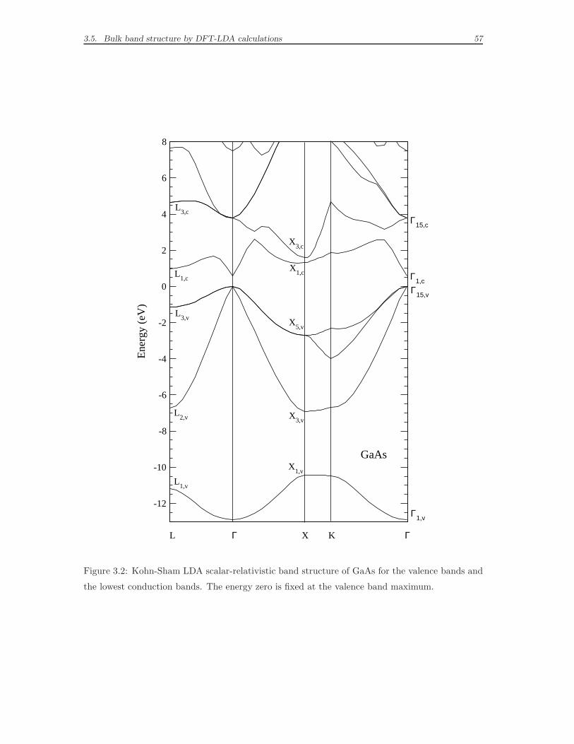
3.5. Bulk band structure by DFT-LDA calculations 57
-12
-10
-8
-6
-4
-2
0
2
4
6
8E
nerg
y (e
V)
L Γ X K Γ
GaAs
Γ1,c
Γ15,v
Γ15,c
Γ1,v
X1,c
X3,c
X5,v
X3,v
X1,v
L1,v
L2,v
L3,v
L1,c
L3,c
Figure 3.2: Kohn-Sham LDA scalar-relativistic band structure of GaAs for the valence bands and
the lowest conduction bands. The energy zero is fixed at the valence band maximum.
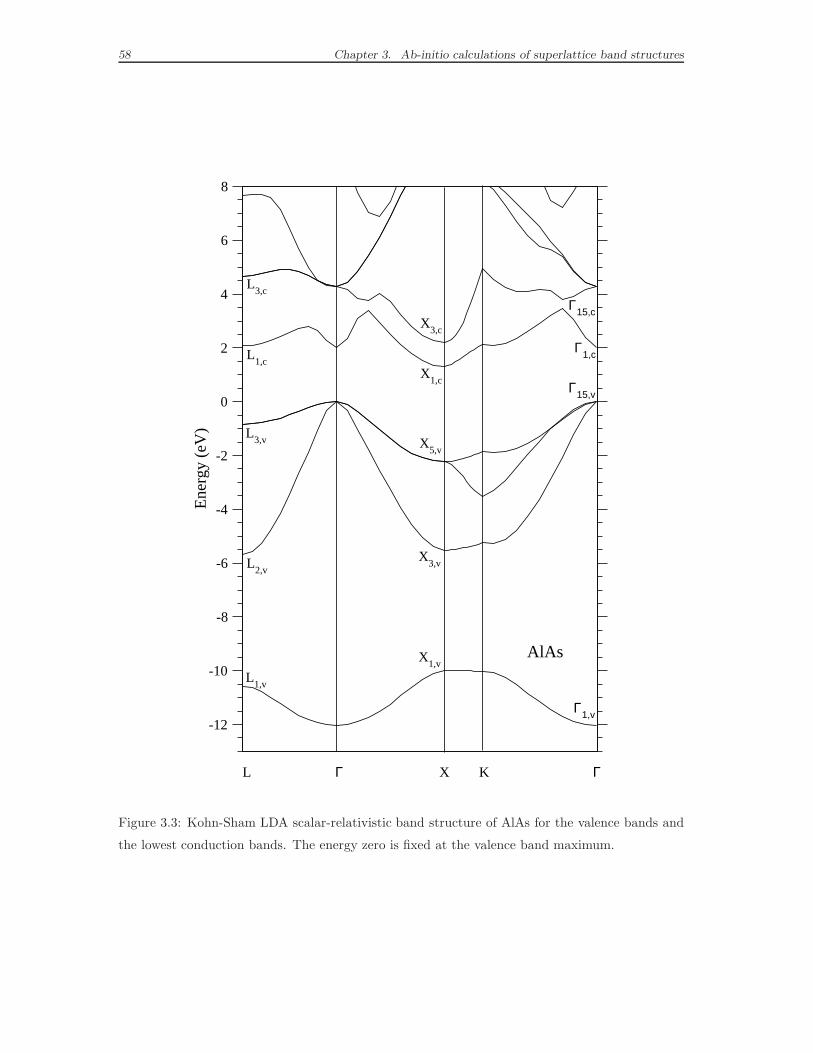
58 Chapter 3. Ab-initio calculations of superlattice band structures
-12
-10
-8
-6
-4
-2
0
2
4
6
8E
nerg
y (e
V)
L Γ X K Γ
AlAs
Γ1,c
Γ15,v
Γ15,c
Γ1,v
X1,c
X3,c
X5,v
X3,v
X1,v
L1,v
L2,v
L3,v
L1,c
L3,c
Figure 3.3: Kohn-Sham LDA scalar-relativistic band structure of AlAs for the valence bands and
the lowest conduction bands. The energy zero is fixed at the valence band maximum.
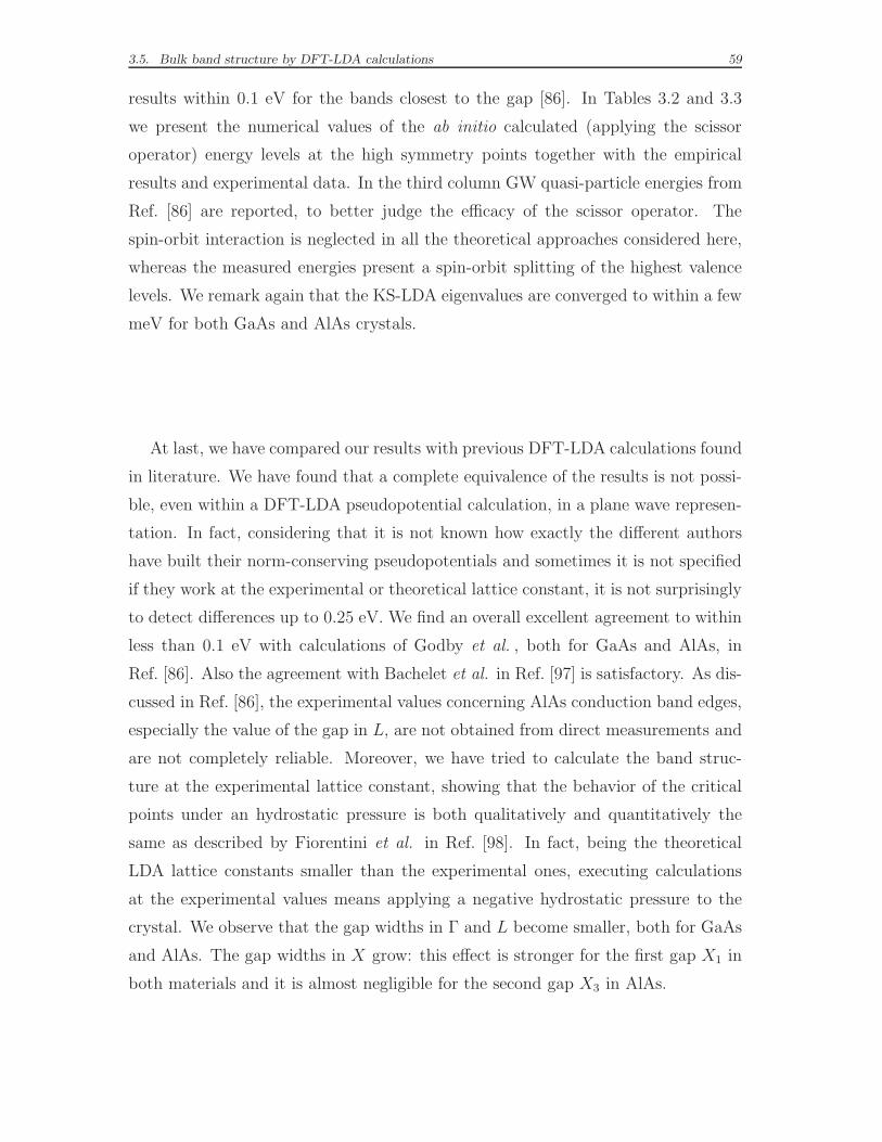
3.5. Bulk band structure by DFT-LDA calculations 59
results within 0.1 eV for the bands closest to the gap [86]. In Tables 3.2 and 3.3
we present the numerical values of the ab initio calculated (applying the scissor
operator) energy levels at the high symmetry points together with the empirical
results and experimental data. In the third column GW quasi-particle energies from
Ref. [86] are reported, to better judge the efficacy of the scissor operator. The
spin-orbit interaction is neglected in all the theoretical approaches considered here,
whereas the measured energies present a spin-orbit splitting of the highest valence
levels. We remark again that the KS-LDA eigenvalues are converged to within a few
meV for both GaAs and AlAs crystals.
At last, we have compared our results with previous DFT-LDA calculations found
in literature. We have found that a complete equivalence of the results is not possi-
ble, even within a DFT-LDA pseudopotential calculation, in a plane wave represen-
tation. In fact, considering that it is not known how exactly the different authors
have built their norm-conserving pseudopotentials and sometimes it is not specified
if they work at the experimental or theoretical lattice constant, it is not surprisingly
to detect differences up to 0.25 eV. We find an overall excellent agreement to within
less than 0.1 eV with calculations of Godby et al. , both for GaAs and AlAs, in
Ref. [86]. Also the agreement with Bachelet et al. in Ref. [97] is satisfactory. As dis-
cussed in Ref. [86], the experimental values concerning AlAs conduction band edges,
especially the value of the gap in L, are not obtained from direct measurements and
are not completely reliable. Moreover, we have tried to calculate the band struc-
ture at the experimental lattice constant, showing that the behavior of the critical
points under an hydrostatic pressure is both qualitatively and quantitatively the
same as described by Fiorentini et al. in Ref. [98]. In fact, being the theoretical
LDA lattice constants smaller than the experimental ones, executing calculations
at the experimental values means applying a negative hydrostatic pressure to the
crystal. We observe that the gap widths in Γ and L become smaller, both for GaAs
and AlAs. The gap widths in X grow: this effect is stronger for the first gap X1 in
both materials and it is almost negligible for the second gap X3 in AlAs.
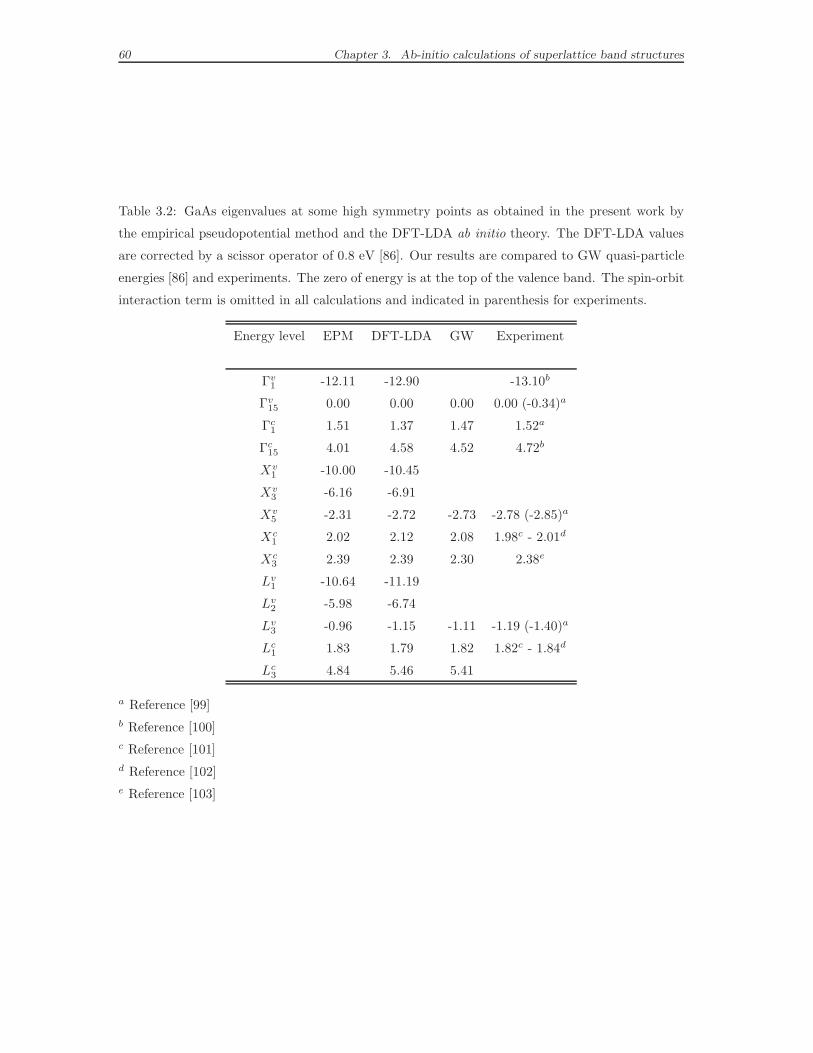
60 Chapter 3. Ab-initio calculations of superlattice band structures
Table 3.2: GaAs eigenvalues at some high symmetry points as obtained in the present work by
the empirical pseudopotential method and the DFT-LDA ab initio theory. The DFT-LDA values
are corrected by a scissor operator of 0.8 eV [86]. Our results are compared to GW quasi-particle
energies [86] and experiments. The zero of energy is at the top of the valence band. The spin-orbit
interaction term is omitted in all calculations and indicated in parenthesis for experiments.
Energy level EPM DFT-LDA GW Experiment
Γv1 -12.11 -12.90 -13.10b
Γv15
0.00 0.00 0.00 0.00 (-0.34)a
Γc1 1.51 1.37 1.47 1.52a
Γc15
4.01 4.58 4.52 4.72b
Xv1 -10.00 -10.45
Xv3
-6.16 -6.91
Xv5 -2.31 -2.72 -2.73 -2.78 (-2.85)a
Xc1
2.02 2.12 2.08 1.98c - 2.01d
Xc3 2.39 2.39 2.30 2.38e
Lv1
-10.64 -11.19
Lv2
-5.98 -6.74
Lv3
-0.96 -1.15 -1.11 -1.19 (-1.40)a
Lc1
1.83 1.79 1.82 1.82c - 1.84d
Lc3
4.84 5.46 5.41
a Reference [99]
b Reference [100]
c Reference [101]
d Reference [102]
e Reference [103]
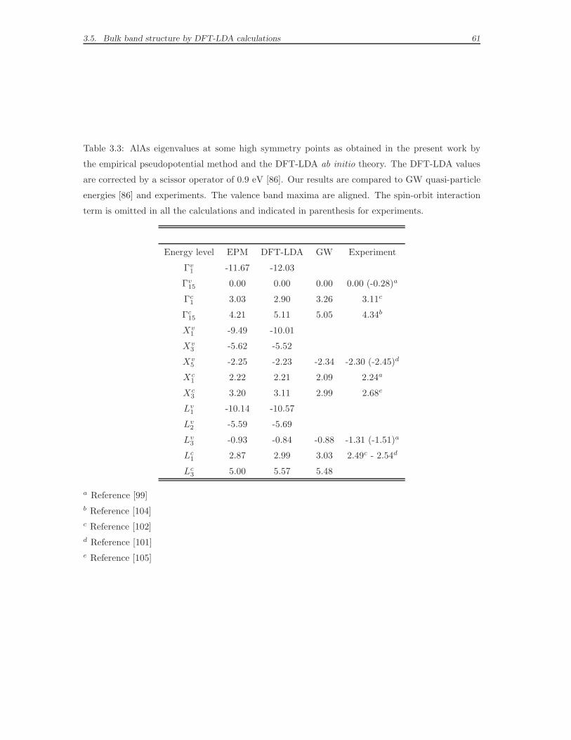
3.5. Bulk band structure by DFT-LDA calculations 61
Table 3.3: AlAs eigenvalues at some high symmetry points as obtained in the present work by
the empirical pseudopotential method and the DFT-LDA ab initio theory. The DFT-LDA values
are corrected by a scissor operator of 0.9 eV [86]. Our results are compared to GW quasi-particle
energies [86] and experiments. The valence band maxima are aligned. The spin-orbit interaction
term is omitted in all the calculations and indicated in parenthesis for experiments.
Energy level EPM DFT-LDA GW Experiment
Γv1 -11.67 -12.03
Γv15
0.00 0.00 0.00 0.00 (-0.28)a
Γc1 3.03 2.90 3.26 3.11c
Γc15
4.21 5.11 5.05 4.34b
Xv1 -9.49 -10.01
Xv3
-5.62 -5.52
Xv5 -2.25 -2.23 -2.34 -2.30 (-2.45)d
Xc1
2.22 2.21 2.09 2.24a
Xc3 3.20 3.11 2.99 2.68e
Lv1
-10.14 -10.57
Lv2
-5.59 -5.69
Lv3
-0.93 -0.84 -0.88 -1.31 (-1.51)a
Lc1
2.87 2.99 3.03 2.49c - 2.54d
Lc3
5.00 5.57 5.48
a Reference [99]
b Reference [104]
c Reference [102]
d Reference [101]
e Reference [105]
62 Chapter 3. Ab-initio calculations of superlattice band structures
3.6 Superlattice band structure by DFT-LDA calculations
Finally, we present ab initio calculations of (001) GaAs/AlAs superlattice band
structures, obtained by means of the DFT-LDA, with norm-conserving pseudopo-
tentials and a plane wave basis set. These calculations are formally analogous to
the calculations for bulk systems presented in the previous section. The cubic Td
point group is replaced by the smaller tetragonal D2d point group and each super-
cell contains p Ga atoms, p Al atoms and 2p As atoms (see Fig. 1.1 on page 11).
The symmetry of the system is fully described: in particular, the As atoms at the
interface do not entail any artificial asymmetry, because the As norm-conserving
pseudopotential is independent of the environment (Ga or Al neighbors) where the
As atoms are placed. We have studied (001) (GaAs)p/(AlAs)p superlattices with a
superlattice period p ranging from 1 to 8. The number of plane waves involved in the
calculations grows as p, thus the computational expense becomes higher and higher
at large superlattice periods (as a term of comparison, on a NEC SX-5 machine,
to compute 10 × 2p bands relative to p=1 the time needed is 2 minutes, whereas
calculating the corresponding number of bands for p=8 requires a time more than
100 times longer).
The resolution of the KS equations for the almost lattice-matched heterostruc-
tures has been done at the averaged theoretical lattice constants. We do not need
to perform a structural minimization to determine the relaxed geometry of the cell,
since the lattice mismatch is small enough to make negligible stress and strain ef-
fects, which do not affect the band structure, as usually assumed in literature (see,
e.g., [106, 107, 108, 109]). We have however verified that the total energy does not
change significantly when moving from the GaAs lattice constant to the AlAs lattice
constant. Moreover, the total energy is close to its minimum at this averaged value.
In Figs. 3.4 and 3.5 we present the two extreme examples of superlattice bands
for p=1 and p=8: all the 4× 2p valence states and the conduction states up to 8 eV
are shown in the tetragonal Brillouin zone. We remind that, since 2p k-points in the
fcc Brillouin zone are always folded onto the same point q in the smaller tetragonal
Brillouin zone, the number of occupied superlattice bands is 2p times the number
of bulk bands for a GaAs/AlAs superlattice. The p=1 superlattice (see Fig. 3.4)

3.6. Superlattice band structure by DFT-LDA calculations 63
-12
-10
-8
-6
-4
-2
0
2
4
6
8
Ene
rgy
(eV
)
R Γ M X Γ Z- - - - - -
(GaAs)1/(AlAs)
1
Figure 3.4: Kohn-Sham LDA scalar-relativistic band structure of a (GaAs)1/(AlAs)1 (001) su-
perlattice along the high symmetry directions. The energy zero is taken at the valence band
maximum.
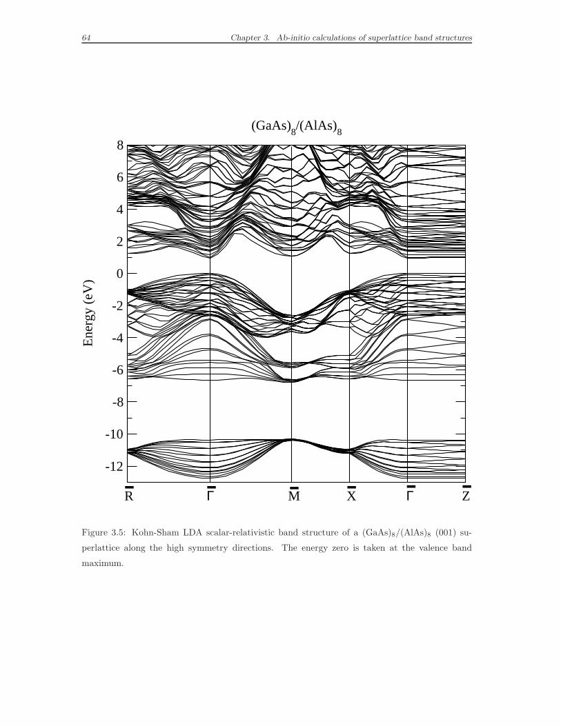
64 Chapter 3. Ab-initio calculations of superlattice band structures
-12
-10
-8
-6
-4
-2
0
2
4
6
8
Ene
rgy
(eV
)
R Γ M X Γ Z- - - - - -
(GaAs)8/(AlAs)
8
Figure 3.5: Kohn-Sham LDA scalar-relativistic band structure of a (GaAs)8/(AlAs)8 (001) su-
perlattice along the high symmetry directions. The energy zero is taken at the valence band
maximum.

3.6. Superlattice band structure by DFT-LDA calculations 65
-12
-10
-8
-6
-4
-2
0
2
4
6
8
Ene
rgy
(eV
)
R Γ M X Γ Z- - - - - -
(GaAs)8/(AlAs)
8
Figure 3.6: Semi-empirical LCBB band structure of a (GaAs)8/(AlAs)8 (001) superlattice along
the high symmetry directions. The energy zero is taken at the valence band maximum.
66 Chapter 3. Ab-initio calculations of superlattice band structures
is the more instructive one, because the number of bands is only doubled and the
figure is more readable and easy to compare to the band structure in Fig. 3.2. This
case was not studied within the semi-empirical framework, because a description
in terms of bulk states is not reliable for very short period superlattices. The p=1
Brillouin zone can be obtained by folding once the bulk zone. Hence, the point Γ
corresponds to both points Γ and Xz, the point M corresponds to both points Xy
and Xx, and point R corresponds to both points Lz and L−z of the corresponding
bulk Brillouin zone. The lowering in the crystal symmetry is responsible for the
removal of level degeneracies at the high symmetry points. The spin orbit splitting
is not included. The direct LDA band gap measures 1.1 eV: it is almost twice larger
than the bulk GaAs gap, pointing to strong confinement effects. The R1c state is the
conduction band minimum, in agreement with the DFT-LDA and quasi-particle re-
sults reported in Refs. [44, 21]. Following the suggestion in Ref. [21], we have applied
a scissor operator of 0.92 eV to calculated conduction band energies and compared
our energies at the high symmetry points with analogous DFT-LDA results, avail-
able only for p=1,2,3, by Dandrea et al. [21]. The differences never exceed 0.1 eV.
The good agreement of short-period results suggests that also the results for larger
periods are reliable. To improve these results, quasi-particle corrections and/or all
electron and/or full relativistic ( including spin-orbit interaction) calculations would
be needed.
Finally, the Fig. 3.6 shows the band structure of the (GaAs)8/(AlAs)8 super-
lattice, as calculated by the semi-empirical LCBB method adopted in the previous
chapter. The Figs. 3.6 and 3.5 are here presented on the same scale, to allow an easy
comparison of the two band dispersions. As expected, the gap is better reproduced
by the semi-empirical calculations. Except for that, the band dispersions and widths
are surprisingly similar, both in valence and in conduction bands.
In conclusions, in this chapter we have presented DFT-LDA calculations for bulk
GaAs, bulk AlAs and GaAs/AlAs superlattices. By calculating the ground states
properties of the bulk materials, we have proved the reliability of the norm-conserving
pseudopotentials we have constructed. The results for bulk LDA energy levels, after
the application of a suitable scissor operator, have been compared with corresponding
results, which we have obtained in the semi-empirical LCBB approach, and with
3.6. Superlattice band structure by DFT-LDA calculations 67
experimental and theoretical data found in literature. The ab initio GaAs/AlAs
band structure is compared to the corresponding semi-empirical band structure and
to some data available in literature for short-period superlattices. We have found an
overall agreement of all the different results, which confirms the analysis developed
in Chapter 1 and attests without doubts the high quality of the electronic states,
both semi-empirical and DFT-LDA, which will be the basis of the optical absorption
calculations in the following chapters.

68 Chapter 3. Ab-initio calculations of superlattice band structures
Chapter 4
Semi-empirical calculations of
optical properties
In a spectroscopic experiment the sample is excited from its ground state: the re-
sponse to the perturbation is the object of both experimental measurements and
theoretical calculations. A big variety of phenomena can occur. In Fig. 4.1 we show
three model excitations: direct photoemission, inverse photoemission, and absorp-
tion. Direct/inverse photoemission processes are one-quasi-particle excitations: a
quantum of energy hν is absorbed/emitted while an electron is ejected/absorbed.
The ejected/incoming electron is supposed to be completely decoupled from the sys-
tem after/before the process takes place. These kinds of experiments give insight,
respectively, on the density of occupied and unoccupied states. Here we are more
interested in absorption processes in solids. In a naive picture, the incoming ra-
diation causes the transition of an electron from an occupied state in the valence
band to an empty state in the conduction band. However, even if one uses quasi-
particle instead of one-electron states, one faces the problem that this process is
not the simple combination of an inverse photoemission and a direct photoemission
process, because the electron does not leave the sample and continues interacting
with it. The electron which has undergone a transition to the conduction band and
the relative hole left in valence band feel each other via a Coulomb interaction: this
is the so-called excitonic effect, which introduces the main complexity in computa-
tions, since it forces to abandon the independent quasi-particle picture, to move to
69
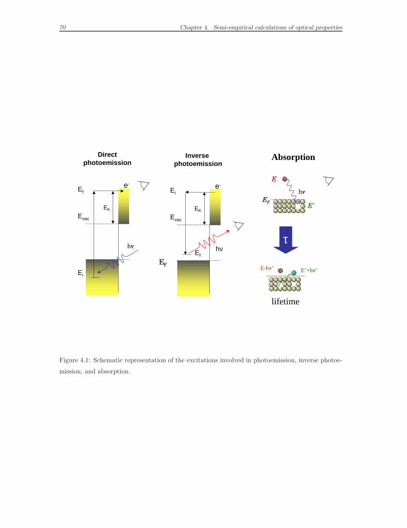
70 Chapter 4. Semi-empirical calculations of optical properties
EF
E
E’
EF
Ei
Evac
EK
Efe-
hν1
Directphotoemission
lifetime
Evac
EF Ef
EK
Eie-
Inversephotoemission
hν
hQ
hQ
Absorption
τ
E-hQ’ E’+hQ’EF
Figure 4.1: Schematic representation of the excitations involved in photoemission, inverse photoe-
mission, and absorption.
71
a two-particle excitation picture.
Nevertheless, in the study of the optical properties, independent particle schemes
maintain their usefulness, and are preliminary to full many-body treatments. The
most used approach is the semi-classical theory of interband transitions [9, 110]. In
this chapter, we will discuss how to combine it with semi-empirical band structure
calculations, to gain information about the absorption spectra of semiconductor su-
perlattices. This simple formalism allows to reproduce all the features present in an
absorption spectrum which are connected to one-quasi-particle excitations. More-
over, it allows to describe the absorption process in terms of the intuitive concepts
of joint density of occupied and unoccupied states and of transition probabilities
from occupied to unoccupied states.
As we have already discussed in Section 3.4, strictly speaking, electrons in a
solid are never independent particles. In spite of this, the one-particle picture can
be retained at the price to renormalize the single electron energy levels by the
presence of the surrounding electrons, defining the concept of quasi-particles. This
is sufficient only for situations where the electron-hole interaction is not important.
The quasi-particles are still described by a one-particle Schrodinger-like equation,
where the effective potential has to include the effects due to the electron-electron
interaction. In case of empirical/semi-empirical band structure calculations, these
renormalizations are at least partially included – to what extent it depends by
the complexity of the model – thanks to the parameterization of the Hamiltonian,
which is directly fitted to reproduce the experimental spectra. On the other hand,
excitonic effects lead inevitably to the need of a two-particle description of the
system. Within an empirical/semi-empirical approach, they can be qualitatively
included thanks to an effective mass approximation [111, 112]. Together with the so-
called local field effects, excitonic effects give essential contributions to estimate the
height of the peaks in absorption spectra. In empirical/semi-empirical calculations,
however, the peak positions can be already in good agreement with experiments
(within a few tenth of eV) without the inclusion of these corrections. In fact, the
empirical parameters can be expressly fitted to reproduce the correct peak positions.
Being mainly interested in determining the peak positions and their evolution as a
function of the well/barrier width, we have decided, at this stage, to neglect both the
72 Chapter 4. Semi-empirical calculations of optical properties
contributions of excitons and local fields. We will discuss at the end of the chapter
the limits of this approximation.
One further point of interest is the birefringence. The calculations presented here
yield only the contribution to the birefringence arising from quantum-confinement-
induced modifications of the electronic states; they do not account for the intrinsic
dielectric anisotropy of a multilayer, arising from different boundary conditions for
an electric field parallel or perpendicular to the layers [113, 114]. This second contri-
bution to the birefringence is in fact equivalent to the inclusion of local-field effects
in the dielectric response [115, 116, 117, 118].
In the following section we will organize the results obtained, discussing the
optical properties of GaAs/AlAs and GaAs/vacuum superlattice systems, via the
calculated real and the imaginary parts of the components of their macroscopic
dielectric tensor. We have written a computational code, which adopts the LCBB
technique, as presented in Chapter 2, to perform the calculations of the optical
spectra. We will explain why the method succeeds in reproducing the experimental
behavior of the peak positions under confinement, whereas it fails to describe the
low-frequency optical birefringence of the GaAs/AlAs systems and, in particular, its
behavior as a function of the number of monolayers p.
4.1 Semi-classical theory of interband transitions
The macroscopic dielectric properties of a solid are intimately connected with its
band structure: we want to discuss how the optical spectra can be reproduced, al-
ready to a satisfactory extent even if at a first level of approximation, starting from
the simple knowledge of the one-electron band structure. The discussion which fol-
lows is valid for isotropic materials, like bulk zinc-blend crystals, where a simple
scalar dielectric function (more precisely its real and imaginary parts) is all we need
to determine the optical response of the medium. In case of anisotropic crystals,
like superlattices, it is necessary to define a dielectric tensor: the expressions we
will get for the dielectric functions are easily adaptable for the single components of
the dielectric tensor. We will deal with an electromagnetic field, which is supposed
weak, acting as a perturbation. The wavelength of the incoming radiation is long in
4.1. Semi-classical theory of interband transitions 73
comparison to the lattice constant and we suppose, at the moment, that the medium
can be considered homogeneous. The theory is called semi-classical because, while
the Bloch electrons are described as a quantum system, the radiation is treated as
a classical field. The core ions are kept “frozen” in their lattice sites, thus excluding
the occurrence of phonon-assisted electronic transitions. Undoubtedly, phonons are
responsible for broadening spectral features: these lifetime effects can be approxi-
mately taken into account by a small imaginary constant added to the absorption
energy.
The complete Hamiltonian, which describes an electron in a solid in presence of
the electromagnetic field, is:
H =1
2
(
v − A(r, t)
c
)2
+ V PP − Φ(r, t) , (4.1)
where A is the vector potential and Φ the scalar potential of the radiation field. In
the Coulomb gauge (∇ · A = 0, Φ = 0), neglecting non-linear effects, the electron-
radiation interaction term reads:
H loce−rad = −1
cA(r, t) · p . (4.2)
The relation (4.2) is correct only if the potential is local (the semi-empirical pseu-
dopotential is local), otherwise we need to take into account the non-vanishing com-
mutator of the non-local term with the coordinate operator:
Hnon−loce−rad = −1
c(p ·A(r, t) + i [Vnl, r] · A(r, t)) . (4.3)
For an incoming plane wave characterized by a frequency ω, the vector potential A
has the form:
A(r, t) = A0 e ei(q·r−ωt) + c.c. , (4.4)
where e is the polarization unitary vector and c.c. indicates the complex conjugate
of the precedent term. The first term in (4.4) is responsible for absorption, the
second for stimulated emission.
Following Bassani and Pastori Parravicini [110], the probability per unit time
and unit volume that a perturbation of the form H e±iωt induces a transition from
an initial state |i〉 to a final state |f〉 is given by the Fermi’s golden rule:
Wi→f (ω) = 2π |〈f |H|i〉|2 δ (ωf − ωi ∓ ω) , (4.5)
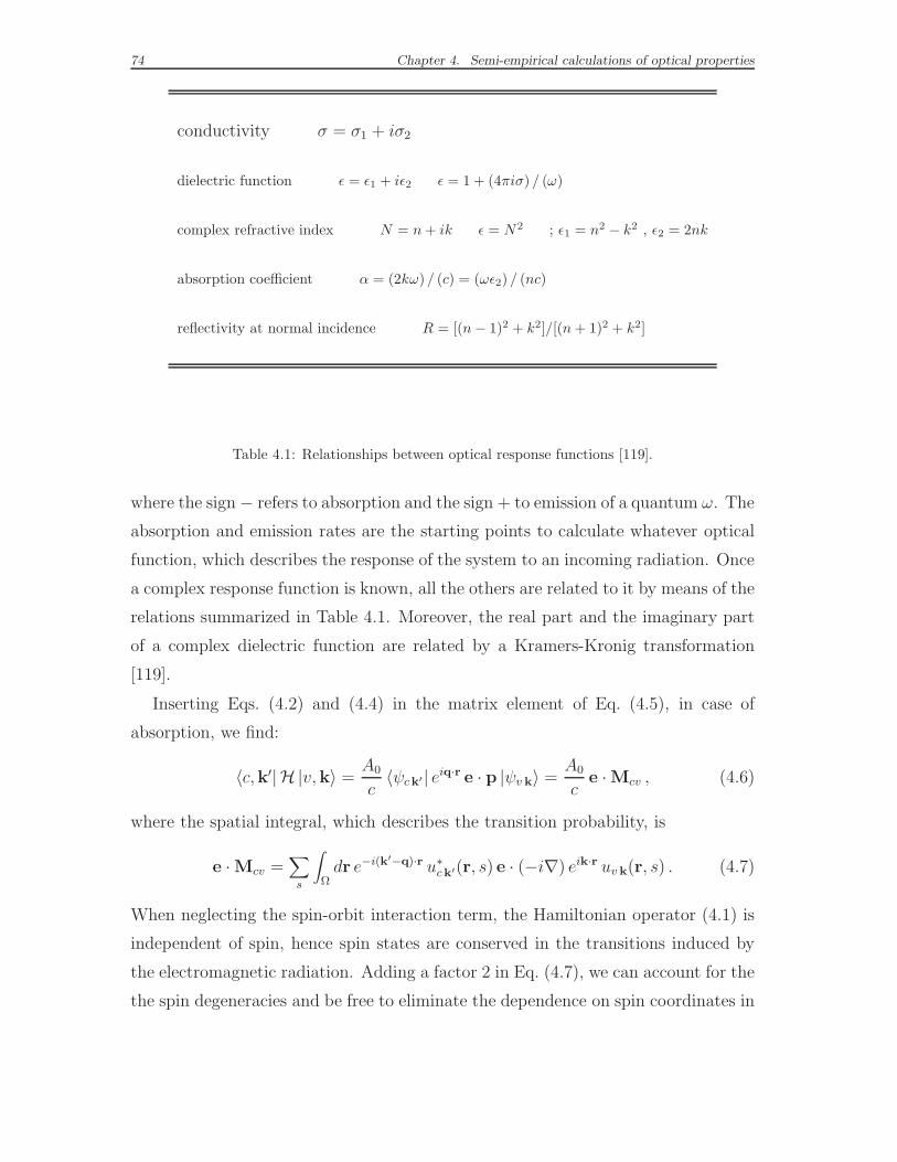
74 Chapter 4. Semi-empirical calculations of optical properties
conductivity σ = σ1 + iσ2
dielectric function ǫ = ǫ1 + iǫ2 ǫ = 1 + (4πiσ) / (ω)
complex refractive index N = n + ik ǫ = N2 ; ǫ1 = n2 − k2 , ǫ2 = 2nk
absorption coefficient α = (2kω) / (c) = (ωǫ2) / (nc)
reflectivity at normal incidence R = [(n − 1)2 + k2]/[(n + 1)2 + k2]
Table 4.1: Relationships between optical response functions [119].
where the sign − refers to absorption and the sign + to emission of a quantum ω. The
absorption and emission rates are the starting points to calculate whatever optical
function, which describes the response of the system to an incoming radiation. Once
a complex response function is known, all the others are related to it by means of the
relations summarized in Table 4.1. Moreover, the real part and the imaginary part
of a complex dielectric function are related by a Kramers-Kronig transformation
[119].
Inserting Eqs. (4.2) and (4.4) in the matrix element of Eq. (4.5), in case of
absorption, we find:
〈c,k′| H |v,k〉 =A0
c〈ψck′ | eiq·r e · p |ψv k〉 =
A0
ce · Mcv , (4.6)
where the spatial integral, which describes the transition probability, is
e · Mcv =∑
s
∫
Ωdr e−i(k′−q)·r u∗ck′(r, s) e · (−i∇) eik·r uv k(r, s) . (4.7)
When neglecting the spin-orbit interaction term, the Hamiltonian operator (4.1) is
independent of spin, hence spin states are conserved in the transitions induced by
the electromagnetic radiation. Adding a factor 2 in Eq. (4.7), we can account for the
the spin degeneracies and be free to eliminate the dependence on spin coordinates in
4.1. Semi-classical theory of interband transitions 75
the matrix element (4.7). The translational invariance of the wavefunction periodic
parts u∗ck′(r, s) and u∗v k(r, s) imposes that, under the hypothesis of long wavelength
λ (q = qrad ≃ 0), only direct transitions, i.e. between valence and conduction states
labelled by the same k vector, are permitted. This selection rule represents the
respect of the momentum conservation in a periodic medium, whereas the energy
conservation is expressed by the presence of the delta function in Eq. (4.5). To
obtain the absorption probability per unit time and per unit volume, it is necessary
to sum over all the possible initial and final states |n,k〉, remembering that the level
occupancy is described by the Fermi function fn,k. We obtain:
Wabs(ω) = 4π(
A0
c
)2∑
v,c
∑
k∈BZ
fvk (1 − fck)∣
∣
∣ e ·Mcv
∣
∣
∣
2δ(
ωc(k)− ωv(k)− ω)
. (4.8)
In a completely analogous way we can get the emission probability per unit time
and unit volume:
Wem(ω) = 4π(
A0
c
)2∑
v,c
∑
k∈BZ
fck (1 − fvk)∣
∣
∣ e ·Mvc
∣
∣
∣
2δ(
ωc(k) − ωv(k) + ω)
. (4.9)
The absorption coefficient is defined as the coefficient α in the relation
I = I0e−αd , (4.10)
which describes the intensity I of the radiation propagating in the medium at a
distance d from the surface: the intensity decreases from the incoming value I0
on the surface, following an exponential law. The determination of the absorption
spectra requires the knowledge of the absorption coefficient, or equivalently, the
imaginary part of the dielectric function ǫ = ǫ1 + iǫ2:
α =ω
ncǫ2 . (4.11)
Here n is the real part of the refractive index. We can obtain α dividing the difference
between the absorbed and the emitted energy per unit time and per unit volume by
the incident radiation flux:
α(ω) =(Wabs −Wem)ω
nA20 ω
2/ 2π c. (4.12)
The following equality is verified:
|e ·Mcv(k)|2 = |e · Mvc(k)|2 ; (4.13)

76 Chapter 4. Semi-empirical calculations of optical properties
it is the quantum formulation of the detailed balance principle. Thus, the final result
for the imaginary part of the dielectric function is:
ǫ2(ω) = 24π2
ω2
∑
c,v
∫
BZ
dk
8π3(fv,k − fc,k) |e · Mcv(k)|2 δ (ωc(k) − ωv(k) − ω) . (4.14)
It is usually preferred to calculate ǫ2 rather than α, because it does not depend on
the index of refraction n, which is a function of the energy ω as well. By exploiting
the Kramers-Kronig transformation, the expression of the real part of ǫ can be
immediately derived from the knowledge of the imaginary part over all the frequency
range (4.14):
ǫ1 (ω) = 1 +2
πP∫ ∞
0
ω′ ǫ2 (ω′)
ω′2 − ω2dω′ . (4.15)
The transition rate depends on the factor |e ·Mcv(k)|2. Close to a critical point, if
the transition is not forbidden, this factor is different from zero and does not vary
significantly with k, so that we can extract it from the integral in (4.14), giving:
ǫ2(ω) =4π2
ω2
∑
c,v
|e · Mcv(k)|2 Jcv(ω)Acv(ω) , (4.16)
where
Acv(ω) = fv,k − fc,k (4.17)
is the band filling factor and
Jcv(ω) =∫
BZ
dk
4π3δ (ωc(k) − ωv(k) − ω) =
1
4π3
∫
S
dS
|∇k (ωc(k) − ωv(k))|ωc−ωv=ω
(4.18)
is the joint density of states (JDOS) for interband transitions. The JDOS shows
strong variations in the neighborhood of the values of ω which satisfy the relation:
∇kωc(k) = ∇kωv(k) . (4.19)
The requirement (4.19) defines the critical points in the Brillouin zone and is usually
satisfied in the high symmetry points or along the symmetry lines. Close to an
extreme k0 of the band dispersion, the energy difference in the denominator of
Eq. (4.18) can be developed in a series of (k − k0), up to the quadratic term in the
expansion. Thanks to this simple analytical procedure, it is possible to deduce the
form of the absorption curves close to the direct gap ωg, in 1, 2 and 3 dimensions:
3D : Jcv(ω) =1
2π2(2m∗)3/2 (ω − ωg)
1/2 θ (ω − ωg) , (4.20)
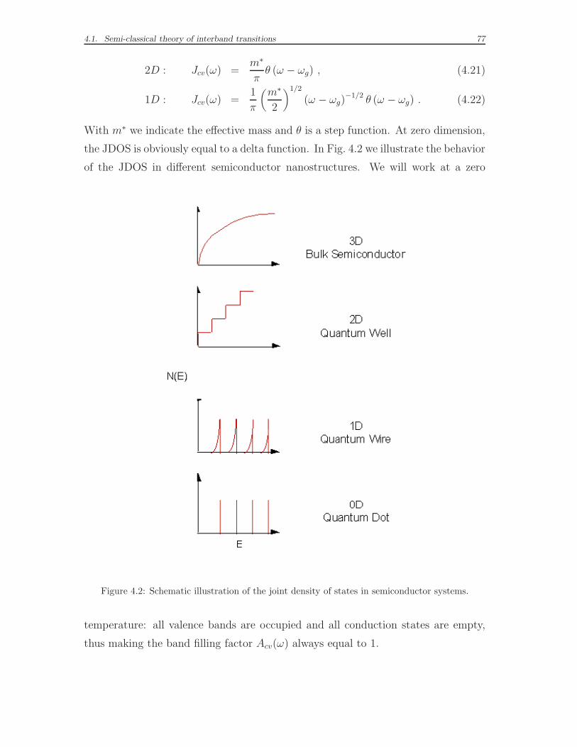
4.1. Semi-classical theory of interband transitions 77
2D : Jcv(ω) =m∗
πθ (ω − ωg) , (4.21)
1D : Jcv(ω) =1
π
(
m∗
2
)1/2
(ω − ωg)−1/2 θ (ω − ωg) . (4.22)
With m∗ we indicate the effective mass and θ is a step function. At zero dimension,
the JDOS is obviously equal to a delta function. In Fig. 4.2 we illustrate the behavior
of the JDOS in different semiconductor nanostructures. We will work at a zero
Figure 4.2: Schematic illustration of the joint density of states in semiconductor systems.
temperature: all valence bands are occupied and all conduction states are empty,
thus making the band filling factor Acv(ω) always equal to 1.
78 Chapter 4. Semi-empirical calculations of optical properties
The polarization unitary vector e in Eq. (4.14) can assume whatever direction
in case of an isotropic material, without affecting the physical properties, which are
not dependent on the orientation of the sample. In case of an anisotropic crystal, a
scalar quantity is no more sufficient to define the optical properties of the material: a
dielectric tensor is needed instead. By choosing e, in three successive steps, along the
three principal optical axes, we can calculate the three components of the diagonal
dielectric tensor of the superlattice.
4.2 Results for bulk optical spectra
GaAs and AlAs present similar absorption properties: this is easy to understand,
remembering that the two bulk semiconductors have extremely similar band struc-
tures (see Figs. 2.2 and 2.3 on pages 25 and 27). Interband absorption spectra of
tetrahedral semiconductors are dominated by two prominent features, denoted E1
and E2 [8, 9]. The E1 peak (and its spin-orbit counterpart E1 + ∆1, which is not
present in our calculated spectra) originates from band-to-band transitions along the
Γ-L direction, where valence and conduction bands are nearly parallel: this results
in a M1-type critical point, i.e. a saddle point in the JDOS, which also gives a strong
excitonic character to the transition. The E2 peak, instead, has contributions from
different parts of the Brillouin zone, but mainly from a region centered around the
special point (34, 1
4, 1
4) (in units of 2π/a, where a is the lattice constant). The E2
peak has essentially no excitonic character. In a superlattice made of alternating
GaAs and AlAs layers (or GaAs and vacuum layers), on the basis of the analysis we
have presented for the superlattice band structures, we expect to recognize again
the same characteristic features. In particular, in the region along the Γ-L direc-
tion, the electrons which contribute to the E1 peak are confined in GaAs layers (see
Fig. 2.5 on page 30). We are interested in comparing the bulk GaAs E1 peak to
the superlattice E1 peaks at different well/barrier widths. In Fig. 4.3 we show the
calculated real and imaginary parts of dielectric functions for bulk GaAs and AlAs
crystals. Starting from the one-electron semi-empirical band structure, the complex
dielectric function ǫ(ω) = ǫ1 + iǫ2 is evaluated in a straightforward way by means
of the semi-classical theory of interband transitions. The curves can be compared
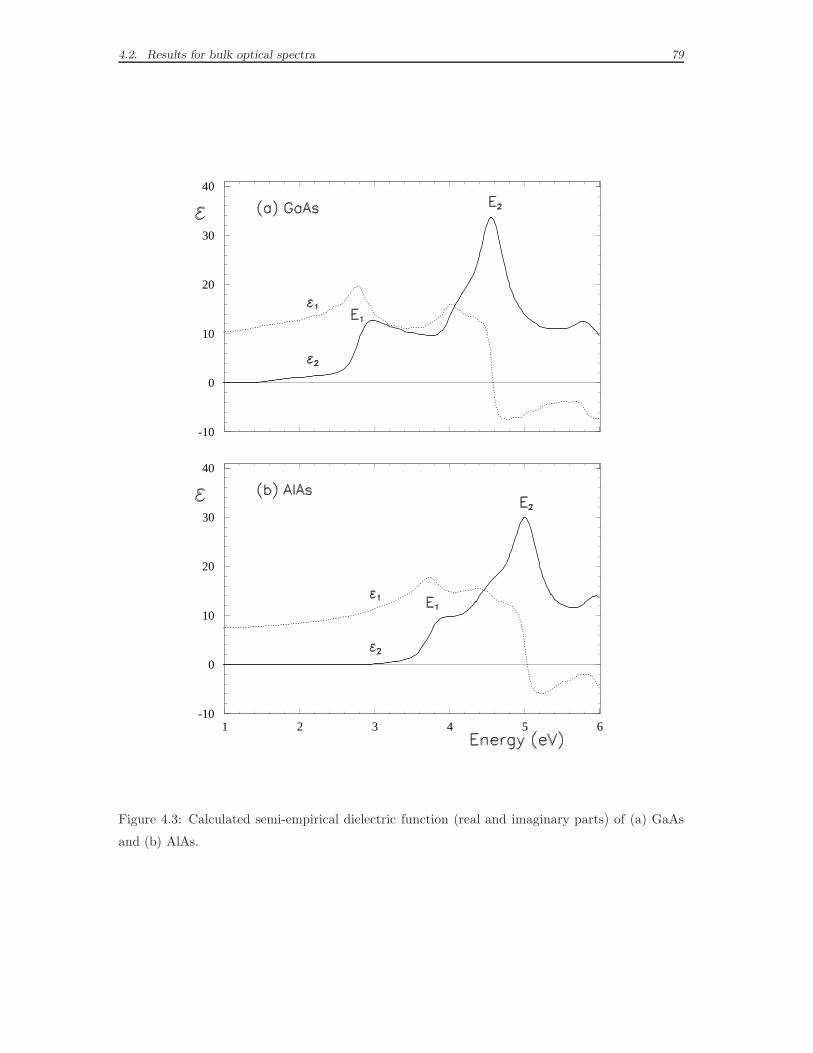
4.2. Results for bulk optical spectra 79
-10
0
10
20
30
40
-10
0
10
20
30
40
1 2 3 4 5 6
Figure 4.3: Calculated semi-empirical dielectric function (real and imaginary parts) of (a) GaAs
and (b) AlAs.
80 Chapter 4. Semi-empirical calculations of optical properties
with analogous measured data [120, 121], shown also later in Figs. 5.5 and 5.6 on
pages 116 and 119. The agreement with the experimental positions of the peaks,
is within a few tenths of an eV: we underline that the semi-empirical approach is
free of the band gap problem. The height of the peaks, especially E1, cannot be
correctly estimated without the inclusion of the excitonic contributions and the local
field effects.
Before calculating superlattice spectra, we have previously calculated bulk spec-
tra for (001) (GaAs)2p, i.e. we have described the cubic material as a periodic
array of tetragonal supercells, repeating the test for different supercell lengths in
the direction z. Integrating over the fcc Brillouin zone and the corresponding folded
tetragonal Brillouin zone, using equivalent sets of Chadi and Cohen special points,
we have verified the exact equivalence of the two results. An empirical Gaussian
broadening of 0.1 eV has been used to produce smooth curves. The spectra obtained
by the two different descriptions of the same system are perfectly superimposable.
This check guarantees now the right to compare the bulk absorption curves with
analogous superlattice curves, knowing that the differences cannot be due to uncon-
trollable errors in the numerical integration.
4.3 Optical spectra for GaAs/AlAs and GaAs/vacuum su-
perlattices
We discuss now the spectra obtained for superlattice systems. Tetragonal Brillouin
zone integrations are performed using Fourier quadrature with 1056 Chadi and Co-
hen special points in the irreducible wedge [64, 122]. The same set of special points
had already been used for bulk (GaAs)2p, to allow a direct comparison of results.
The experimental broadening is simulated again by an empirical Gaussian broaden-
ing of 0.1 eV. The calculated imaginary part of the dielectric function ǫ2 (ω) for both
GaAs/AlAs and GaAs/vacuum systems are shown in Fig. 4.4 for different super-
lattice periods p. At this stage we are not interested in the absorption anisotropy,
thus we average over the three orthogonal polarization directions to obtain a scalar
dielectric function. Like the optical spectra of bulk GaAs and AlAs, superlattice
spectra show two prominent features, namely E1 and E2 peaks (see Fig. 4.3): in
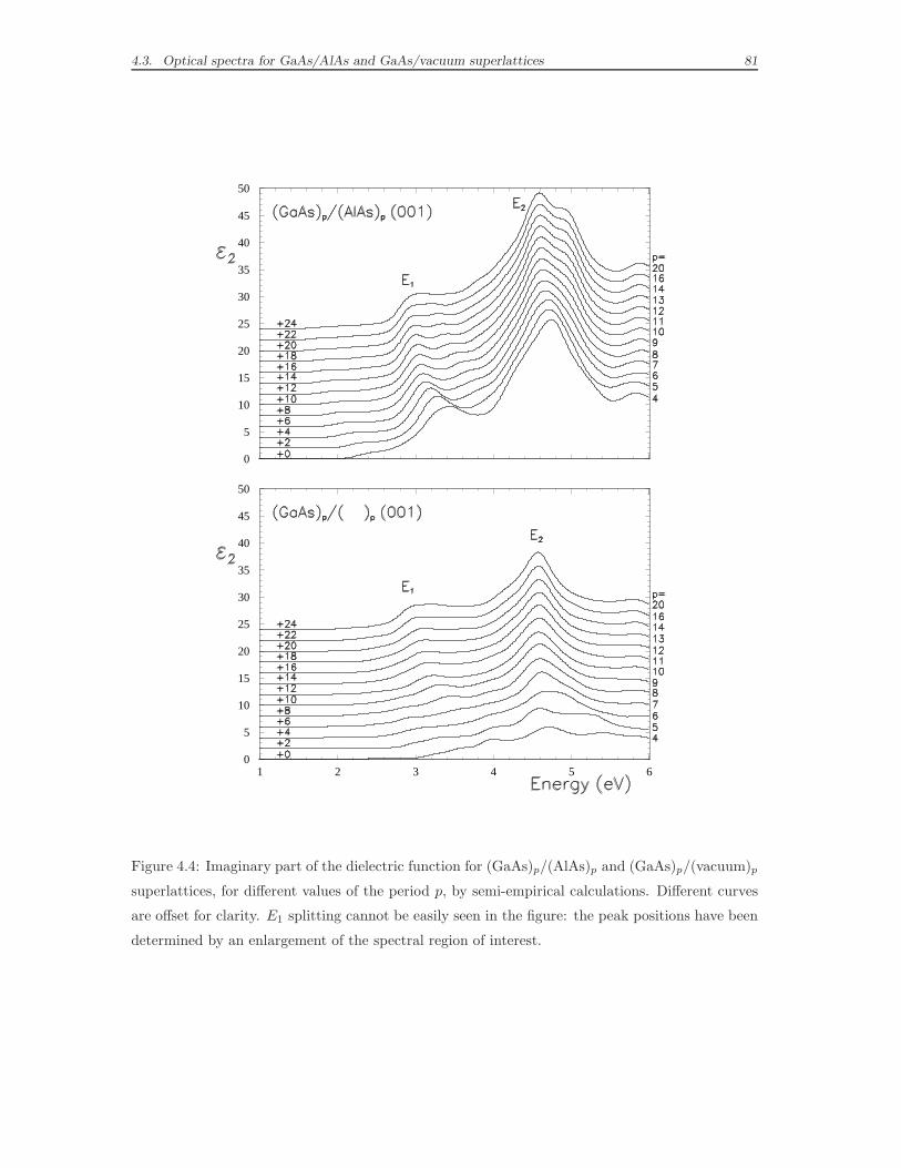
4.3. Optical spectra for GaAs/AlAs and GaAs/vacuum superlattices 81
0
5
10
15
20
25
30
35
40
45
50
0
5
10
15
20
25
30
35
40
45
50
1 2 3 4 5 6
Figure 4.4: Imaginary part of the dielectric function for (GaAs)p/(AlAs)p and (GaAs)p/(vacuum)p
superlattices, for different values of the period p, by semi-empirical calculations. Different curves
are offset for clarity. E1 splitting cannot be easily seen in the figure: the peak positions have been
determined by an enlargement of the spectral region of interest.
82 Chapter 4. Semi-empirical calculations of optical properties
fact, even if in a superlattice selection rules allow more transitions, as a consequence
of zone-folding, the tetragonal Brillouin zone is smaller and, at last, all transitions
which contribute to superlattice peaks have their equivalent counterparts in the bulk
Brillouin zone. Another way to understand the similarity between bulk and super-
lattice optical spectra is to remember how close the superlattice band dispersion
in Fig. 2.6 on page 33 is to the bulk band dispersion projected on the tetragonal
Brillouin zone in Fig. 2.4 on page 28. As a general remark, the E1 transition is
found to blue shift and to split into two peaks for decreasing superlattice periods;
the confinement-induced shift is larger for the GaAs/vacuum system. On the other
hand the E2 transition is split for large-period GaAs/AlAs superlattices, where the
electronic states are confined in the two bulk layers leading to a superimposition of
the two bulk spectra; the two peaks merge into a single one for small periods. A
single E2 peak with a small blue shift is found for GaAs/vacuum superlattices.
In Fig. 4.5 the peak energies are plotted as a function of the superlattice period
p. First we comment on the behavior of E1: in zinc-blend crystals it comes from
transitions along the Λ line, in a region where bulk bands are almost parallel. When
the system is confined in the [001] direction, it is not intuitive to describe the con-
sequences of folding along 〈111〉 directions. The calculated spectra show that along
the folded Λ line transitions subdivide in two main groups and lead to a splitting
of the E1 peak in the absorption curves. The two peaks have different oscillator
strengths and, except for an intermediate period length, the lowest energy one be-
comes much stronger and covers the other one. Both peaks undergo confinement
effects and are moved towards higher energies in comparison with their bulk posi-
tion: the confinement and the consequent shifts are stronger at smaller well widths.
A splitting of the E1 transition with a blue shift of both peaks was indeed observed
experimentally in GaAs/AlAs superlattices [10]. In the present calculation this is
attributed to a splitting of the bulk valence band at the point L and along the Λ-
line, as indicated by the band energies. The results of Figs. 4.4 and 4.5 show also
that E1 peak displacements are more relevant in GaAs/vacuum superlattices, where
quantum confinement effects are stronger due to the vacuum barrier.
The behavior of the E2 peak is substantially different: its main contribution
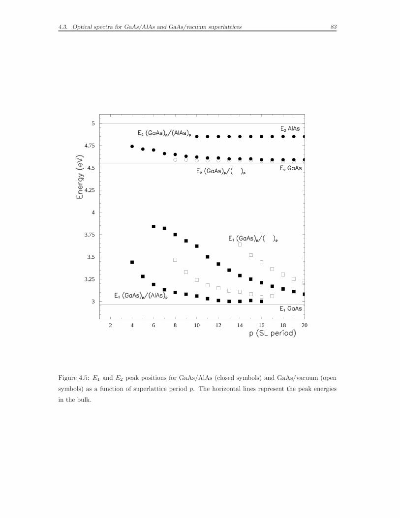
4.3. Optical spectra for GaAs/AlAs and GaAs/vacuum superlattices 83
3
3.25
3.5
3.75
4
4.25
4.5
4.75
5
2 4 6 8 10 12 14 16 18 20
Figure 4.5: E1 and E2 peak positions for GaAs/AlAs (closed symbols) and GaAs/vacuum (open
symbols) as a function of superlattice period p. The horizontal lines represent the peak energies
in the bulk.
84 Chapter 4. Semi-empirical calculations of optical properties
comes from transitions in a region close to the special point k = 2πa
(
34, 1
4, 1
4
)
1. At
this k-point the alignment of both valence and conduction GaAs and AlAs bands is
almost flat and the electronic wave functions are completely delocalized all over the
heterostructure. This explains why E2 peak in GaAs/AlAs superlattices is at an
intermediate energy between bulk GaAs and AlAs E2 peak positions and does not
shift when the superlattice period p decreases. Our calculated peak positions are in
good agreement with experimental data [123, 10, 11], and in particular a splitting
of E2 is reported in Ref. [11]. In GaAs/vacuum superlattices the situation changes:
the electrons near the special point are confined in GaAs layers and the superlattice
E2 peak has a weak blue shift at small superlattice periods p, going back to the bulk
GaAs E2 energy when p grows. A single peak obviously arises in this case since
there is no AlAs contribution. At last, we present in Fig. 4.6 some curves for the
real part of the dielectric function ǫ1 for GaAs/AlAs heterostructures. We observe
that the average, or Penn gap (defined as the energy at which ǫ1 goes through
zero) does not depend on the superlattice period. This proves that the center of
gravity of valence and conduction bands is preserved, as suggested in Ref. [16]: this
follows from compensating effects of a blue shift at the bottom of the band (positive
curvature) and a red shift at the top of the band (negative curvature).
4.4 Optical anisotropy and macroscopic dielectric tensor
In (GaAs)p/(AlAs)p (001) superlattices the Td cubic point group of the zinc-blend
structure is replaced by the D2d symmetry group. Cubic crystals present isotropic
optical properties, while in a superlattice the reduction in symmetry leads to optical
anisotropy in the real part of the dielectric constant (birefringence) and in the imag-
inary part (absorption anisotropy, or dichroism). The optical response can no longer
be characterized by a complex dielectric function, in its place a complex dielectric
tensor must be introduced. The GaAs/AlAs system is uniaxial, with the optical
axis directed along the growth direction z, thus the dielectric tensor has the form:
ǫij (ω) = ǫii (ω) δij , (4.23)
1What we call E2 peak may in fact contain weak contributions from the E′
0transition, which can be clearly
resolved only in derivative spectra. See e.g. Refs.[8, 10].
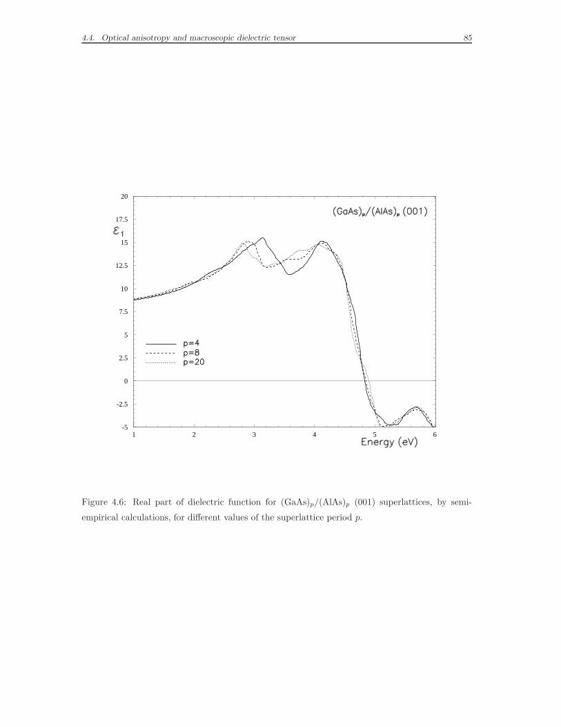
4.4. Optical anisotropy and macroscopic dielectric tensor 85
-5
-2.5
0
2.5
5
7.5
10
12.5
15
17.5
20
1 2 3 4 5 6
Figure 4.6: Real part of dielectric function for (GaAs)p/(AlAs)p (001) superlattices, by semi-
empirical calculations, for different values of the superlattice period p.
86 Chapter 4. Semi-empirical calculations of optical properties
where ǫxx = ǫyy = ǫ⊥ and ǫzz = ǫ‖2.
However, we do not hide that there are further complications. Besides the effects
of spatial anisotropy, there are effects due to the spatial inhomogeneity of the solid,
independently of his symmetry group. These are the local field effects, which will
be discussed in the next chapter (see Section 5.2). The inclusion of local fields in
calculations allow to account naturally for the intrinsic dielectric anisotropy of a
multilayer, arising from different boundary conditions for an electric field parallel
or perpendicular to the layers [113, 114]. This contribution to birefringence can
be estimated for long wavelength of the incoming radiation and large superlattice
periods p, in a classical effective medium model [27]. If boundaries are assumed
abrupt and the constituent materials are supposed to conserve their bulk dielectric
functions up to the interfaces, we can apply approximate expressions for ǫ⊥ and ǫ‖
in terms of bulk constituent scalar dielectric functions, ǫ1 and ǫ2 [113]:
ǫ⊥ (ω) =1
l1 + l2(ǫ1 (ω) l1 + ǫ2 (ω) l2) , (4.24)
ǫ−1‖ (ω) =
1
l1 + l2
(
l1ǫ1 (ω)
+l2
ǫ2 (ω)
)
, (4.25)
where l1, l2 are the layer thicknesses of the two different materials. Using semi-
empirical calculated values of bulk static dielectric constants in expressions (4.24)
and (4.25) we find a rough estimate ∆n ≃ 0.03 for the local field contribution to
birefringence at zero frequency. We know that this sizeable contribution at large
superlattice periods will be missed in our calculations, as long as we neglect local
field effects. Local field effects are known to depend on the superlattice period 3.
At this stage we decide not include local field effects: we directly take into account
only the effects of electronic confinement and band folding on optical transitions.
Comparison with birefringence data from Ref. [16], reported in Fig. 4.9, should allow
to determine if the confinement and the band folding contributions to anisotropy
2In GaAs/vacuum superlattices, where the point group is C2v , the system is biaxial with principal axes along
[110], [110], [001] and the dielectric constant for in-plane polarization has a slight additional anisotropy. The
situation is analogous to heterostructures with no-common atom, where the in-plane anisotropy has been measured
[124].3The macroscopic treatment remains valid as long as the superlattice period remains much smaller than the
wavelength of light, otherwise the superlattice should better be viewed as a one-dimensional photonic crystal, where
local-field effects embodied in ǫ(G,G′) lead to the formation of a band gap for light propagation [125].
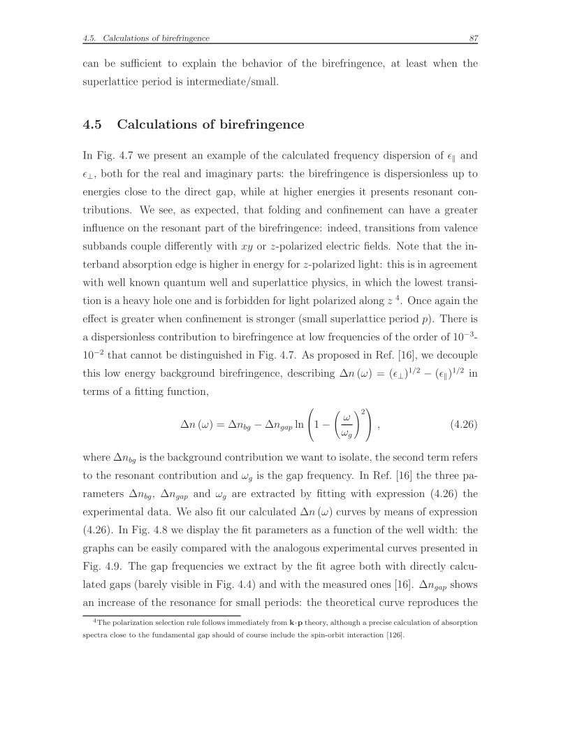
4.5. Calculations of birefringence 87
can be sufficient to explain the behavior of the birefringence, at least when the
superlattice period is intermediate/small.
4.5 Calculations of birefringence
In Fig. 4.7 we present an example of the calculated frequency dispersion of ǫ‖ and
ǫ⊥, both for the real and imaginary parts: the birefringence is dispersionless up to
energies close to the direct gap, while at higher energies it presents resonant con-
tributions. We see, as expected, that folding and confinement can have a greater
influence on the resonant part of the birefringence: indeed, transitions from valence
subbands couple differently with xy or z-polarized electric fields. Note that the in-
terband absorption edge is higher in energy for z-polarized light: this is in agreement
with well known quantum well and superlattice physics, in which the lowest transi-
tion is a heavy hole one and is forbidden for light polarized along z 4. Once again the
effect is greater when confinement is stronger (small superlattice period p). There is
a dispersionless contribution to birefringence at low frequencies of the order of 10−3-
10−2 that cannot be distinguished in Fig. 4.7. As proposed in Ref. [16], we decouple
this low energy background birefringence, describing ∆n (ω) = (ǫ⊥)1/2 − (ǫ‖)1/2 in
terms of a fitting function,
∆n (ω) = ∆nbg − ∆ngap ln
1 −(
ω
ωg
)2
, (4.26)
where ∆nbg is the background contribution we want to isolate, the second term refers
to the resonant contribution and ωg is the gap frequency. In Ref. [16] the three pa-
rameters ∆nbg, ∆ngap and ωg are extracted by fitting with expression (4.26) the
experimental data. We also fit our calculated ∆n (ω) curves by means of expression
(4.26). In Fig. 4.8 we display the fit parameters as a function of the well width: the
graphs can be easily compared with the analogous experimental curves presented in
Fig. 4.9. The gap frequencies we extract by the fit agree both with directly calcu-
lated gaps (barely visible in Fig. 4.4) and with the measured ones [16]. ∆ngap shows
an increase of the resonance for small periods: the theoretical curve reproduces the
4The polarization selection rule follows immediately from k·p theory, although a precise calculation of absorption
spectra close to the fundamental gap should of course include the spin-orbit interaction [126].
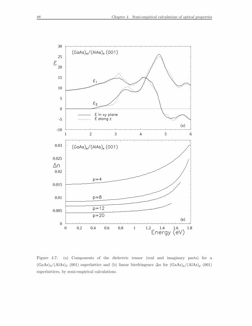
88 Chapter 4. Semi-empirical calculations of optical properties
-10
-5
0
5
10
15
20
25
30
1 2 3 4 5 6
0
0.005
0.01
0.015
0.02
0.025
0.03
0 0.2 0.4 0.6 0.8 1 1.2 1.4 1.6 1.8
Figure 4.7: (a) Components of the dielectric tensor (real and imaginary parts) for a
(GaAs)4/(AlAs)4 (001) superlattice and (b) linear birefringence ∆n for (GaAs)p/(AlAs)p (001)
superlattices, by semi-empirical calculations.
4.5. Calculations of birefringence 89
1.5
1.55
1.6
1.65
1.7
1.75
1.8
1.85
1.9
0
0.001
0.002
0.003
0.004
0.005
0.006
0.007
0.008
0.009
0.01
20 25 30 35 40 45 50 55
Figure 4.8: Parameters of equation (4.26) as a function of well width (half of a superlattice period):
(a) energy gap, (b) ∆ngap and ∆nbg. The results can be compared with the analogous experimental
graphs in Fig. 4.9.

90 Chapter 4. Semi-empirical calculations of optical properties
Figure 4.9: Experimental parameters of equation (4.26) as a function of well width (half of a
superlattice period): (a) energy gap, (b) ∆ngap and ∆nbg from Ref. [16]
4.5. Calculations of birefringence 91
trend of the experimental curve, although the calculated values are significantly
smaller. The sudden decrease of the measured background birefringence ∆nbg be-
low 40 A, on the other hand, is completely missing in our results. Moreover, the
calculated magnitude of this term above 40 A is remarkably underestimated. The
fact suggests that folding effects give only a minor contribution, while the origin of
the behavior of ∆nbg must be attributed to local field effects, as already suggested
in Ref. [16]. Similar considerations can be made for the GaAs/vacuum systems.
The magnitude of the background birefringence related to local field effects can
be estimated in the case of a long wavelength of the incident radiation and a not
too small superlattice period p, thanks to the expressions in (4.24) and (4.25). The
obtained value, i.e. 0.03, is much larger than the calculated values in Fig. 4.8, for all
superlattice periods p, and it is of the same order of magnitude as the the experimen-
tal results at intermediate/large p. Only for small periods p, when relations (4.24)
and (4.25) do not hold, the local field correction may not respect the analytic limit
value. Nevertheless, the effects included in calculations fail to describe the small
superlattice period region as well. Further calculations of the optical properties
including local-field effects are obviously required to clarify this point.
In this chapter we have applied the semi-empirical LCBB technique and the semi-
classical theory of interband transitions to cast light on how the optical spectra of
bulk semiconductors evolve to superlattice spectra. We have discussed the adopted
approximations, namely the independent-particle picture neglecting local field effects.
First, we have considered the average dielectric function. Quantum-confinement
induced shifts of the critical point energies are calculated for both kinds of super-
lattices and are found to be larger for the GaAs/vacuum systems, where coupling
between different GaAs layers is only due to quantum-mechanical tunneling and has
a negligible effect. For both GaAs/AlAs and GaAs/vacuum superlattices, the E1
peak in the absorption spectrum splits into two peaks with increasing blue shifts for
decreasing superlattice period. This result agrees with the observations of Ref. [10]
on GaAs/AlAs superlattices, and is attributed to a symmetry splitting of the valence
bands along the line Γ-L. The blue shifts are always larger for the GaAs/vacuum
systems. The E2 transition instead is found to be split for large-period GaAs/AlAs
superlattices, where the electronic states of the bulk are confined in each layer and
92 Chapter 4. Semi-empirical calculations of optical properties
the absorption spectrum is the superimposition of the two bulk ones. The energy of
the E2 peak depends weakly on the superlattice period. The average or Penn gap,
defined as the first zero of the real part of the dielectric constant, does not depend
on the superlattice period, confirming the expectation that a blue shift at the lower
absorption edges is compensated by red shifts in the upper parts of the absorption
spectrum.
Second, we have studied the optical anisotropy. The band contribution to linear
birefringence of GaAs/AlAs superlattices is calculated and compared with recent ex-
perimental results of Ref. [16]. The zero-frequency birefringence is found to be much
smaller than the experimental results: we suppose that the missing contribution to
observed static birefringence may be attributed to local-field effects, as already sug-
gested in the experimental analysis of Ref. [16]. The frequency-dependent part of
the birefringence arising from band folding and quantum confinement increases with
decreasing superlattice period, as found in the experiment, although the calculated
values are smaller. Once again, a better qualitative agreement could be obtained
thanks to the inclusion of local field effects.
The presented results state the validity of the LCBB method, and its underlying
approximations, to describe the averaged optical properties. Nevertheless, a deeper
study is needed to understand optical anisotropy, in particular the origin of the
behavior of the static birefringence as a function of the superlattice period.
Chapter 5
Ab-initio calculations of optical
properties
After having discussed the empirical approach, we are going to turn our interest
to first principle theoretical and computational tools in spectroscopic properties
calculations. We have introduced in the previous chapter the complex problem of
determining optical spectra in the whole visible region. A completely satisfactory
solution of this task requires a description, which takes into account at the same
time not only the detailed electronic structure, but also the many-body effects and
the microscopic inhomogeneity of the medium. Non-trivial systems, like surfaces,
clusters, semiconductor nanostructures, are today successfully treated in the ab ini-
tio framework, most often by constructing the excitation spectrum of the system as a
sum over independent transitions between the states determined in the ground state
calculation (i.e. using the one-electron energies and wavefunctions of the Kohn-Sham
equation). This degree of approximation can be equivalent to the one adopted in
our semi-empirical calculations of the optical spectra, which has provided a detailed
analysis of the effects of band folding and confinement in semiconductor superlat-
tices [28]. However, no quantitative agreement with the experiment has been found
concerning the static birefringence, nor could semi-empirical independent-transition
calculations explain, even qualitatively, the increase of the static birefringence with
increasing superlattice period. One might suspect that the semi-empirical approach
is not sufficiently precise to describe such a small effect as the birefringence. The
93
94 Chapter 5. Ab-initio calculations of optical properties
other strongly suspected reason for failure is the inadequacy of the basic approx-
imations used to determine the macroscopic dielectric function. In particular, we
expect that the local field effects can play a very important role. Both the points
call for a more detailed investigation into the anisotropy of the optical response.
In order to go beyond the simple independent-transition picture for the descrip-
tion of two-particle excitations, like absorption spectroscopy, the most important
corrections to be included are the full electron-electron and electron-hole interac-
tions and local field effects. Let us discuss now more in detail these effects. Local
field effects express the fact that, related to the inhomogeneity of the material, its
response to an external potential with given spatial frequency will include, in prin-
ciple, all other spatial frequencies determined by the reciprocal lattice vectors of the
periodic system. This implies that, technically, the size of the problem which has to
be dealt with is considerably bigger than for the simple sum of transitions and, in
fact, local field effects are often omitted in calculations. However, superlattices are
intrinsically inhomogeneous, and these effects can therefore be expected to play an
important role in their optical and dielectric properties. The Kohn-Sham eigenvalues
are not meant to describe electron addition and removal energies: only quasi-particle
energies, which can be obtained within the many-body theory, are suitable to de-
scribe the changes in total energy occurring in direct and inverse photoemission
processes. However, quasi-particle corrections are still not enough to describe all
the effects arising in an absorption process, where interacting electron-hole pairs are
created. In fact, another effect, well known to be important for optical spectra, is
the electron-hole interaction, or excitonic effect. This effect is due to the fact that
the created electron-hole pair may interact more or less strongly, leading to bound
states within the gap and/or to strong deformations above the continuum absorption
edge. The importance of these effects depends on the size of the screening of the
electron-hole interaction and on the details of the band structure. In particular for
flat bands, which are linked to the existence of localized (confined) states, this effect
is expected to be very strong. Hence, due to the confinement properties of superlat-
tices, their spectra are expected to show relevant excitonic effects. At the moment
we want to focus on the superlattice birefringence at zero frequency and not on the
whole absorption spectra: as the static birefringence is a ground state property, we
95
can expect that neglecting quasi-particle corrections and excitonic effects has not a
dramatic influence on the results. As a matter of fact, we will show that only when
local field effects are included qualitative and even quantitative agreement with the
experiment can be achieved. These results will be discussed in the first part of this
chapter.
In the second part, we will go back to the problem of electron-electron and
electron-hole interactions, to study the line-shape of absorption spectra up to 7
eV for bulk GaAs and AlAs systems. The calculation of optical spectra for bulk
semiconductors is a widely investigated subject. In the last decades the many-
body perturbation theory has produced expressions both for the self-energy and the
electron-hole interaction, which are successfully used in computational physics. The
self-energy Σ is usually obtained within Hedin’s GW approach, starting from DFT
results as a zero-order solution. Similarly, the excitonic effects are well described by
the Bethe-Salpeter equation (BSE), via a functional derivative of the self-energy Σ.
However, the many-body perturbation theory is not the only approach developed
to deal with response properties. The limits of DFT comes from the fact that ex-
cited states, are not accessible through static ground state DFT. In principle, these
problems can be overcome, at least as far as optical excitations are concerned, by
taking into account the fact that in the absorption experiment the system is re-
sponding to a time-dependent external field. Therefore a generalization of static
DFT to Time-Dependent DFT (TDDFT) has been proposed [127, 128], i.e. all po-
tentials are now functionals of the time-dependent density. Besides the potentials,
also their functional derivatives with respect to the density are needed (at least
implicitly), since the system is responding self-consistently to the applied perturba-
tion. As it happened in static DFT, again, the main problem resides in finding a
good approximation to the exchange-correlation contribution. The time-dependent
DFT approach still keeps the advantage of the static one to be computationally
very efficient, and could in principle replace other successful, but more cumbersome
methods like the Bethe-Salpeter approach (BSE)[129, 130, 131, 132]. However, there
are some additional difficulties with respect to the case of static DFT: in the present
chapter we will mainly deal with the determination of reliable approximations for
the time-dependent density variation of the exchange-correlation potential Vxc, i.e.

96 Chapter 5. Ab-initio calculations of optical properties
the so-called exchange-correlation (xc) kernel, fxc = δVxc/δρ.
Real calculations are dependent on the chosen approximation for the xc kernel
fxc: the lowest level of approximation (RPA) consists in neglecting the kernel, an-
other simple approximation is the adiabatic local density approximation (TDLDA)
[133, 134], where the kernel is calculated from the LDA exchange-correlation po-
tential V LDAxc . At present, the simple adiabatic local density approximation for the
TDDFT kernel has given promising results for finite systems, but does not succeed
in describing absorption spectra in solids. Improvements might come through the
inclusion of dynamical (memory) effects and/or long-range nonlocal terms [128, 135].
Recently, Reining et al. [30] have shown that a static long-range contribution (LRC)
can simulate the strong continuum excitonic effect in the absorption spectrum of
bulk Silicon. Here we present the results for GaAs and AlAs spectra. We will show
that the optical absorption, which exhibits a strong continuum exciton effect, is
considerably improved with respect to calculations where the adiabatic local den-
sity approximation is used.
We underline that the calculations concerning the superlattice zero-frequency bire-
fringence have been performed within a time-dependent DFT formalism as well.
Also in this case, we will discuss the different approximations adopted to describe
the xc kernel fxc.
5.1 Time Dependent Density Functional Theory
We discuss here the essential formalism of the time-dependent generalization of DFT.
For detailed information on this subject, we suggest to refer to some recent reviews
[128, 136, 137, 138, 139]. The Density Functional Theory, as described in Chapter
3, is a ground state theory, thus unable to account for electronic excitations. These
restrictions can be overcome within the DFT formalism, generalizing it by allowing
a time dependence for the external field. As in classical mechanics, the DFT ground
state is determined by the energy minimum:
δE[ρ]/δρ(r) = 0 . (5.1)
Extending the analogy, as the trajectory of a classical system is given by the extrema
of the classical action∫ t1t0dtL(t), where L is the Lagrangian, the evolution of a

5.1. Time Dependent Density Functional Theory 97
quantum system, which undergoes an external time-dependent potential Vext(r, t),
is given by the extrema of the quantum mechanical action:
A =∫ t1
t0dt〈Ψ(t)|i ∂
∂t− H(t)|Ψ(t)〉 . (5.2)
Of course, there are some theorems [127], exactly analogous to the Hohenberg-
Kohn theorems (see Section 3.1.1) and presented within a framework similar to
the Kohn-Sham scheme (see Section 3.1.2). A first theorem proves that there is a
bijective correspondence between time-dependent external potentials Vext(r, t) and
v-representable time-dependent densities ρ(r, t). A second theorem proves that the
evolution of the system is determined by the extrema of the quantum mechanical
action. Van Leeuwen [140] has shown that the time-dependent density, which char-
acterizes a many-body system can be, in principle, reproduced by a time-dependent
external potential, in a many-body system with no two-particle interactions. This
property allows to represent at any time the density of a many-body system by means
of a non-interacting system, which reproduce the exact interacting density ρ(r, t).
The evolution of the system is described by the time-dependent KS-equations:
[
−1
2∇2 + Veff(r, t)
]
ψi(r, t) = i∂
∂tψi(r, t) , (5.3)
ρ(r, t) =N∑
i=1
|ψi(r, t)|2 , (5.4)
where
Veff(r, t) = VH(r, t) + Vxc(r, t) + Vext(r, t) (5.5)
is, as in the static case, the effective potential felt by the electrons. It consists of the
sum of the external time-dependent applied field, the time-dependent Hartree term,
plus the exchange-correlation potential (defined through the equivalence between the
interacting and fictitious non-interacting systems). From the variational principle,
it is possible to define:
Vxc(r, t) =δAxc[ρ]
δρ(r, t), (5.6)
where Axc[ρ] is the exchange-correlation part of the action functional A. Besides its
elegance, the most remarkable quality of the time dependent DFT is in its compu-
tational simplicity, in comparison to other available methods.
98 Chapter 5. Ab-initio calculations of optical properties
5.1.1 Derivation of an expression for the dielectric function
The linear response of the charge density to an external time-dependent perturbation
is determined by the polarizability χ of the medium:
χ(r, t, r′, t′) =δρ(r, t)
δVext(r′, t′)
∣
∣
∣
∣
∣
Vext=0
. (5.7)
The Eq. (5.7) means that the density ρ(r, t) and the external potential are related
in the following way :
ρ(r, t) = ρ(r, t0) +∫
χ(r, t, r′, t′)Vext(r′, t′)dr′dt′ + O(V 2
ext) . (5.8)
The independent-particle polarization χ0 relates, in a fully equivalent way, the elec-
tron density ρ(r, t) to the effective potential Veff(r, t):
χ0(r, t, r′, t′) =
δρ(r, t)
δVeff(r′, t′)
∣
∣
∣
∣
∣
Veff =0
. (5.9)
Remembering the definition of the effective-potential, Veff = Vext + VH + Vxc, it is
easy to obtain:
δVeff(r, t)
δVext(r′, t′)= δ(r − r′)δ(t− t′)+
∫
[
δ(t− t′′)
|r− r′′| + fxc(r, t, r′′, t′′)
]
χ(r′′, t′′, r′, t′)dr′′dt′′ , (5.10)
where
fxc(r, t, r′, t′) =
δVxc[ρ(r, t)]
δρ(r′, t′)
∣
∣
∣
∣
∣
Vext=0
(5.11)
is the time-dependent xc kernel and
v(x, x′) = v(r, r′) δ(t− t′) =δ(t− t′′)
|r − r′′| (5.12)
accounts for the variation of the Hartree potential. After deriving the simple relation:
δρ/δVext = (δρ/δVeff)(δVeff/δVext) ≡ χ0δVeff/δVext , (5.13)
a Dyson-like equation, which connects the two polarizabilities χ and χ0, follows in
a straightforward way:
χ(r, r′;ω) = χ0(r, r′;ω)+
∫
dr1dr2χ0(r, r1;ω)
[
1
|r1 − r2|+ fxc(r1, r2, ω)
]
χ(r2, r′;ω) . (5.14)
5.1. Time Dependent Density Functional Theory 99
This scheme allows to describe the exact linear response of an interacting system in
terms of the response of a non-interacting system with external potential Veff(r, t).
The exact exchange-correlation contributions are of course unknown, and the appli-
cation of the theory relies on some approximations. The lowest level of approxima-
tion (RPA) consists in neglecting the kernel:
fRPAxc = 0 . (5.15)
Another simple approximation is the adiabatic local density approximation (TDLDA)
[133, 134], where the kernel is calculated from the LDA exchange-correlation poten-
tial used in ground state calculations:
fTDLDAxc (r) = δ (r, r′)
dV LDAxc (r)
dρ(r). (5.16)
Inverting formally Eq. (5.14), one obtains a compact equation
χ = [1 − χ0(v + fxc)]−1 χ0 , (5.17)
where v is the Coulomb potential. The inverse dielectric function ǫ−1 measures the
screening in the system:
ǫ−1 (r, t, r′, t′) =δVeff(r, t)
δVext(r′, t′). (5.18)
In practice, we need the inverse dielectric function in the momentum space, which
is related by a Fourier transform to real space:
ǫ−1 (r, r′;ω) =1
(2π)3
∫
BZdq
∑
G,G′
ei(q+G)·r ǫ−1GG′ (q, ω) e−i(q+G′)·r′ . (5.19)
Some care must be taken in the origin of the induced screening. If the probe is
assumed to be a test particle, it is only affected by the electrostatic Hartree term
in equation (5.10). From Eq. (5.10) it follows that the inverse dielectric function is
connected to the polarizability by the relation:
ǫ−1 = 1 + vχ . (5.20)
The random phase approximation (RPA) response function is obtained, simply
imposing fxc = 0:
ǫ−1RPA = 1 + v (1 − χ0v)
−1 χ0 . (5.21)
100 Chapter 5. Ab-initio calculations of optical properties
Then, inverting the matrix relation and using the matrix equality
(1 − χ0v)−1 χ0 = χ0 (1 − vχ0)
−1 , (5.22)
we obtain:
ǫRPA = 1 − vχ0 . (5.23)
In conclusion, all we need to perform calculations is an explicit formulation of
the polarizability. Application of first-order perturbation theory to the Kohn-Sham
equations (3.20) yields the standard result for the independent-particle polarization
χ0 in the Adler-Wiser formulation [115, 116]:
χ0 (r, r′;ω) = 2∑
i,j
(fi − fj)φi(r)φ
∗j(r)φ
∗i (r
′)φj(r′)
ǫi − ǫj − ω − iη, (5.24)
where fi are the occupation numbers (0, 1) and η is a positive infinitesimal number.
The small imaginary constant added in the denominator accounts for causality,
and describes lifetime effects when it is small, but finite; the factor 2 stems from
spin degeneracy. The explicit Fourier transformation of the independent-particle
polarization results:
χGG′
0 (q, ω) = 2∑
i,j
(fi − fj)〈j|e−i(q+G)·r|i〉〈i|ei(q+G′)·r′|j〉
ǫi − ǫj − ω − iη. (5.25)
5.1.2 RPA approximation without local field effects
It is interesting to establish a link between the formula (4.14) in Section 4.1. for
the imaginary part of the dielectric function and the analogous formula within the
RPA approximation, which we can derive starting from the expression for χ0 in
Eq. (5.25). At this stage, we continue neglecting local field effects, to preserve the
correspondence with the semi-empirical calculations. From Eqs. (5.23) and (5.25)
we obtain:
ǫM (ω) = 1 + 24π
Ω
limq→0
1
q2
∑
k∈BZ
∑
v,c
|〈nc,k + q|eiq·r|nv,k〉|2
ǫnc,k+q − ǫnv,k − (ω + iη)+
|〈nc,k − q|e−iq·r|nv,k〉|2
ǫnc,k−q − ǫnv ,k + (ω + iη)
,
(5.26)
5.1. Time Dependent Density Functional Theory 101
where we have used the Fourier transformation of the Coulomb potential:
1
|r| =4π
Ω
∑
q,G
ei(q+G)·r
|q + G|2. (5.27)
Since the second term (anti-resonant) does not contribute to the absorption, we can
reject it:
ǫ2 (ω) = 24π
Ωlimq→0
1
q2
∑
k∈BZ
∑
nv,nc
Im
|〈nc,k + q|eiq·r|nv,k〉|2
ǫnc,k+q − ǫnv ,k − (ω + iη)
. (5.28)
For a non-local Hamiltonian H , the commutator with the coordinate operator is
given by:d
dtri = i [H, ri] = pi + i [Vnl, ri] , (5.29)
where Vnl is the non-local part of the Hamiltonian. Another way to write the previous
expression is [141]:
vα = limq→0
[
H, eiqrα
]
/q , (5.30)
where vα and rα are, for α = x, y, z, the Cartesian components of v and r. Applying
now Eqs. (5.29) and (5.30) to simplify Eq. (5.28), we obtain
limq→0
〈nc,k + q|eiq·r|nv,k〉/q =e · 〈nc,k|∇i + i [Vnl, r] |nv,k〉
ǫKSc − ǫKS
v
, (5.31)
where e is a polarization unitary vector, pointing in the direction of q. We have indi-
cated explicitly that the eigenvalues in the denominator are Kohn-Sham eigenvalues,
because they derive by the application of the Kohn-Sham Hamiltonian, even if GW
corrections are added. In fact, the use of the quasi-particle Hamiltonian to calculate
the commutator would be much more demanding, because the self-energy operator
Σ is non-local and dynamical. Hence, the final formula in the RPA approximation,
neglecting local field effects is:
ǫ2 (ω) = 24π
Ω
limq→0
∑
k∈BZ
∑
nv,nc
∣
∣
∣
∣
∣
e · 〈nc,k|∇i + i [Vnl, r] |nv,k〉ǫKSc − ǫKS
v
∣
∣
∣
∣
∣
2 [1
ǫnc,k+q − ǫnv,k − (ω + iη)
]
.
(5.32)
We want to show that the expression (5.28) is equivalent to the expression (4.14):
ǫ2(ω) = 24π2
Ω
1
ω2
∑
nc,nv
∑
k∈BZ
|e ·Mcv(k)|2 δ (ωc(k) − ωv(k) − ω) . (5.33)
102 Chapter 5. Ab-initio calculations of optical properties
Exploiting once again Eqs. (5.29) and (5.30), we can rewrite it in a slightly different
way:
ǫ2(ω) = 24π2
Ωlimq→0
1
q2
∑
nc,nv
∑
k∈BZ
∣
∣
∣〈nc,k + q|eiq·r|nv,k〉∣
∣
∣
2δ (ωc(k) − ωv(k) − ω) ,
(5.34)
which is the imaginary part of Eq. (5.28). In fact:
limη→0
1
x± iη= P
1
x∓ iπδ (x) . (5.35)
5.2 Local field effects
A solid which possesses lattice-potential symmetry is non-homogeneous on the mi-
croscopic scale, even when it is characterized by a cubic symmetry group, which
yields isotropic optical properties. When an external perturbing field of small wave
vector q and frequency ω is applied to the system, the local field will in general
contain “Bragg reflected” terms, i.e. dependent on the wave vector q + G, where G
is a reciprocal lattice vector. These microscopically varying terms fluctuate on the
wavelength of the interatomic spacing. The frequency ω is not affected, supposing
the homogeneity of the time. The difference between the local and the macroscopic
field constitutes the local-field corrections in the electromagnetic response.
Let us consider an electric field E, incoming on a non-homogeneous medium.
In the linear approximation, the polarization effects are described by the electric
displacement vector D:
D(q + G, ω) =∑
G′
ǫmic(q + G,q + G′;ω)E(q + G′, ω) . (5.36)
We are interested in a relation which, in the limit of a negligible q, consider only
macroscopic quantities:
DM(ω) = ǫM(ω)EM(ω) . (5.37)
According to Adler [115] and Wiser [116], the macroscopic dielectric tensor can be
related to the inverse of the microscopic dielectric matrix [117, 118]:
ǫM (ω) = limq→0
1
ǫ−1GG′ (q, ω)
∣
∣
∣
∣
∣
G=G′=0
. (5.38)
5.3. Results for the birefringence of GaAs/AlAs superlattices 103
The difference between an homogeneous and non-homogeneous medium lies in the
off-diagonal terms. In the direct space this means that the microscopic dielectric
function ε(r, r′) depends explicitly on the positions r and r′, and not simply on
the distance |r − r′|. If the medium were homogeneous, the macroscopic dielectric
function would be
ǫM = limq→0
ǫG=0,G′=0 , (5.39)
i.e. the spatial average of the microscopic dielectric function. In case of isotropic
media, the direction in which the limit of the small q vector has to be taken is
non-influent. In case of a GaAs/AlAs superlattice, taking the limit of q in the z or
x/y directions gives respectively the components ǫ‖ and ǫ⊥ of the dielectric tensor,
which include local field effects (LFE).
5.3 Results for the birefringence of GaAs/AlAs superlat-
tices
The reduction of the original cubic symmetry of the diamond or zinc-blend struc-
ture gives rise to an optical anisotropy in GaAs/AlAs superlattices [16]. As we
have already discussed in the previous chapter, the birefringence in perturbed bulk
semiconductors has two well-known contributions [142, 143], namely a dispersionless
term related to virtual direct transitions involving high energy gaps between valence
and conduction bands, and a resonant term which represents the isolated effects of
the virtual transitions associated with the small energy gaps between the top valence
bands and the first conduction bands. We have calculated the static birefringence
of (001) (GaAs)p/(AlAs)p superlattices for the barrier/well period p=1 to p=8, em-
ploying the ab initio DFT approach which should a priori describe details of the
band structure in a more reliable way, if compared to an empirical approach. In
fact, one might suspect that the semi-empirical approach is not sufficiently precise
to describe such a quantity as the birefringence which requires calculations of high
precision, being a very small (of the order of 10−2) difference between two dielectric
constants. However, we will see that this rather technical point turns out not to
be the main source of error in the calculations in Chapter 4. We have proved in
Section 5.1.2 that TDDFT calculations without local field effects, within the RPA
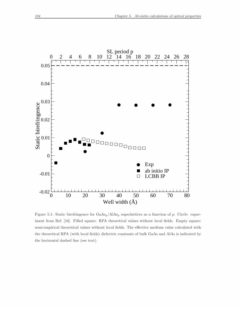
104 Chapter 5. Ab-initio calculations of optical properties
0 10 20 30 40 50 60 70 80Well width (Å)
-0.02
-0.01
0
0.01
0.02
0.03
0.04
0.05
Sta
tic b
irefr
inge
nce
Expab initio IPLCBB IP
0 2 4 6 8 10 12 14 16 18 20 22 24 26 28SL period p
Figure 5.1: Static birefringence for GaAsp/AlAsp superlattices as a function of p. Circle: exper-
iment from Ref. [16]. Filled square: RPA theoretical values without local fields. Empty square:
semi-empirical theoretical values without local fields. The effective medium value calculated with
the theoretical RPA (with local fields) dielectric constants of bulk GaAs and AlAs is indicated by
the horizontal dashed line (see text).

5.3. Results for the birefringence of GaAs/AlAs superlattices 105
approximation for the xc-kernel, yield optical spectra totally equivalent to the ones
we have calculated within the semi-empirical framework. In Fig. 5.1 we compare
ab initio and semi-empirical calculations without local field effects. The two curves
show the same trend as a function of the superlattice period p. The values of the
birefringence are moreover completely compatible: the TDDFT calculations con-
firm hence the semi-empirical results. In our ab initio calculation we have carefully
checked the symmetries of the wavefunctions and of the energy levels. In particular,
the symmetry operation which makes x and y axes equivalent for a tetragonal super-
lattice belongs to a non-symmorfic point group, whereas the codes used can consider
only symmorfic point groups. Thus, we had to work on improving the convergence
of the wavefunctions, to assure that the x and y components of the dielectric tensor
could be equal up to 10−5, and, as a consequence, that the calculated birefringence
could not contain uncontrolled errors due to asymmetries.
It is well known that many-body effects beyond the simple independent-particle
picture often drastically alter the dielectric properties of materials. Self-energy and
excitonic effects can have a significant contribution to the absorption spectra of
even simple bulk semiconductors, and by consequence also change their dielectric
constants. These effects are due to variations of the exchange-correlation potential
upon excitation. Of course, there are also contributions stemming from variations
of the Hartree potential, including the so-called local field effects, which express
the fact that these variations reflect the charge inhomogeneity of the responding
material. Therefore, local field effects can be of moderate importance, compared
to the exchange-correlation contributions, for example in the absorption spectra of
simple bulk semiconductors, but show up increasingly when one considers more in-
homogeneous systems. In electronic spectra of clusters (which are to be considered
as a strong inhomogeneity in empty space), and for spectra involving excitations
from strongly localized states [144], local field effects alone explain already most
of the drastic disagreement between results obtained in the independent-transition
approach, and the experimental spectra. One can hence suspect that, as already
suggested by [16] and indirectly confirmed by the results of the previous chapter,
local field effects play a crucial role for the description of the anisotropy of the di-
electric properties of superlattices, and should not be neglected, independently of
106 Chapter 5. Ab-initio calculations of optical properties
the fact whether semi-empirical or ab initio approaches are used. Thus, we have
decided to investigate the role of local field effects. The RPA values of the bire-
fringence ∆n =√ε⊥ − √
ε‖ calculated without and with local fields (respectively
empty and filled squares) are reported on Fig. 5.2 as a function of the well width,
together with the experimental results of Ref. [16] (filled circles). Once again, we re-
mark that the neglect of local fields leads to an anisotropy much smaller than in the
experiment. The inclusion of the off-diagonal elements in the inversion of ε−1G,G′ dras-
tically changes the behavior of the birefringence: the amplitude increase up to the
expected effective medium value ∆n = 0.05, calculated with ε⊥ = (εGaAs + εAlAs)/2
and ε−1‖ = (ε−1
GaAs + ε−1AlAs)/2 [27]. Since any calculation of the static dielectric
constant within the RPA approximation, increases the dielectric mismatch between
GaAs and AlAs compared to experiment [145], the effective medium plateau calcu-
lated with theoretical dielectric constants has a higher value than the experimental
one. The inclusion of local field effects perfectly reproduces the increase of the
anisotropy with increasing superlattice period, which was completely absent in the
independent-transition calculations. We find that, for p > 3, the optical anisotropy
in (GaAs)p/(AlAs)p superlattices is completely determined by the anisotropy of the
local fields.
It is now interesting to analyze these results more in detail, in order to under-
stand better the importance of local field effects. Eqs. (5.25) and (5.23) show that,
indeed, χ0 and the microscopic RPA dielectric tensor εRPA are sums over indepen-
dent transitions, but the relation between the macroscopic dielectric constant and
χ0 (even in RPA) is much more complicated than the simple linear relation (5.23),
that is used in calculations neglecting local field effects. The inversion (5.38) leads
in fact to an effective mixing of transitions. Therefore, it is worthwhile to see, as
a first step, which transitions determine the anisotropy of the dielectric response.
We explore this idea by examining the effects of the highest valence and lowest con-
duction bands on the birefringence for the well/barrier period p=3 and p=8. In a
first step we consider ”all” the conduction bands (i.e. those necessary to achieve
convergence) as possible final states for the transitions, but we restrict the initial
states to the v first valence bands (Fig. 5.3, lower panel). Note that in order to scale
the results of the three superlattices, the abscissa axis varies from lattice to lattice,
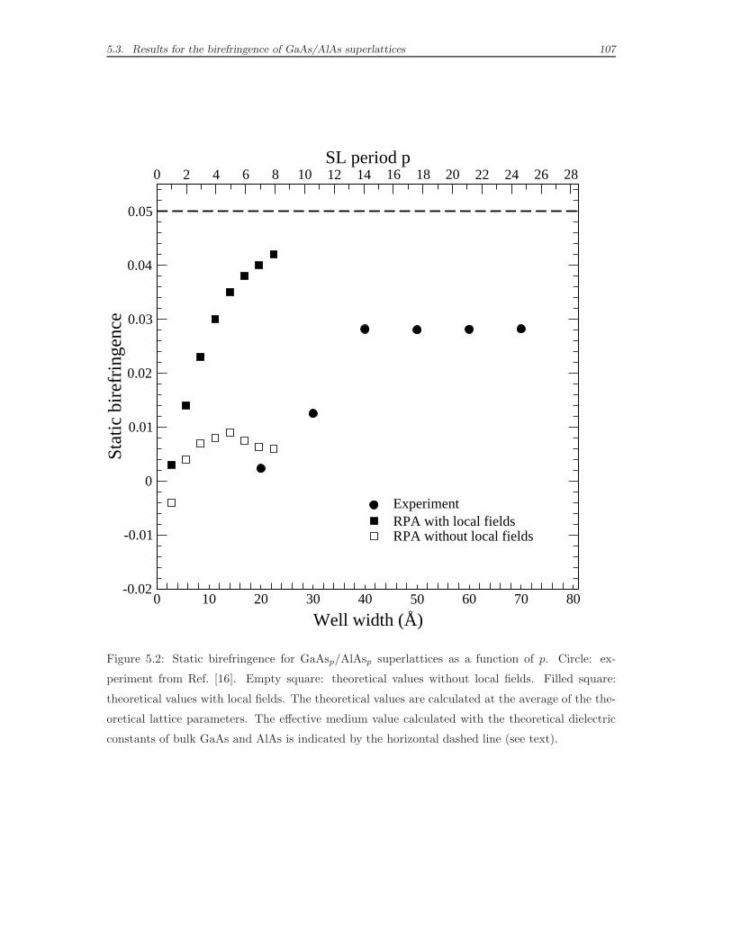
5.3. Results for the birefringence of GaAs/AlAs superlattices 107
0 10 20 30 40 50 60 70 80
Well width (Å)
-0.02
-0.01
0
0.01
0.02
0.03
0.04
0.05
Sta
tic b
irefr
inge
nce
ExperimentRPA with local fieldsRPA without local fields
0 2 4 6 8 10 12 14 16 18 20 22 24 26 28SL period p
Figure 5.2: Static birefringence for GaAsp/AlAsp superlattices as a function of p. Circle: ex-
periment from Ref. [16]. Empty square: theoretical values without local fields. Filled square:
theoretical values with local fields. The theoretical values are calculated at the average of the the-
oretical lattice parameters. The effective medium value calculated with the theoretical dielectric
constants of bulk GaAs and AlAs is indicated by the horizontal dashed line (see text).
108 Chapter 5. Ab-initio calculations of optical properties
with v = ip, p being the well/barrier period and i an integer. The dependence of the
birefringence on the number of valence bands included in the calculation shows the
same behavior for all the studied superlattices. The bands 1 to 2p do not contribute
to the birefringence. A large positive contribution arises from bands 4p to 6p, which
is almost completely canceled by the (folded) light-hole and heavy-hole bands from
6p to 8p. If local field effects are neglected the cancellation is total. Also the con-
tributions of the bands to the birefringence due to the local fields cancel, and even
lead to a change in sign; the final results is dominated by the anisotropy of the local
fields arising from transitions involving the top valence bands.
In a second step, we consider ”all” the valence bands, and restrict final states
to the c upper conduction bands as final states (Fig. 5.3, upper panel). Here the
conduction band number is c = (i − 1)p + 1, and i and p have already been de-
fined. The highest conduction bands do not contribute to the birefringence. The
high step-like positive contribution of the intermediate bands are canceled by the
(folded) last conduction bands. Once again, the local fields are not important but
for the bottom conduction bands. The cancellation effects are essential: in fact,
a calculation involving only the highest valence and the lowest conduction bands
yields a contribution of local field effects which is overestimated by about a factor
10. The observed anisotropy can hence not be explained in a simple model involving
few transitions. The evolution of the top valence region is most characteristic for
what is going on in this system: due to the anisotropy, to be precise the confine-
ment in z-direction, the top valence at Γ splits into a double degenerate heavy-hole
and a single light-hole state. We find that the light hole state at Γ couples to light
polarized along the growth direction, whereas the heavy-hole states respond to light
polarized in-plane. Of course, the order and character of the states change through-
out the Brillouin zone, which prevents a simple one-to-one analysis, but, as it is also
evident from Fig. 5.4, this lifting of degeneracy in the region close to the Fermi level
is sufficient to explain the observed anisotropies in calculations without local field
effects.
A deeper analysis of the birefringence passes through an analysis of its single
components, i.e. the dielectric constant for light polarized in plane and perpendic-
ular to the growth direction. In Fig. 5.4 the upper panel shows the results for ǫ⊥
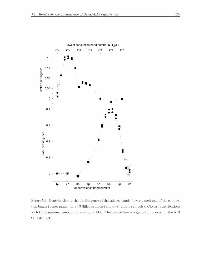
5.3. Results for the birefringence of GaAs/AlAs superlattices 109
1p 2p 3p 4p 5p 6p 7p 8pUpper valence band number
0
0.1
0.2
0.3
0.4
stat
ic b
irefr
inge
nce
i=1 i=2 i=3 i=4 i=5 i=6 i=7
Lowest conduction band number (i−1)p+1
0
0.04
0.08
0.12
0.16
stat
ic b
irefr
inge
nce
Figure 5.3: Contribution to the birefringence of the valence bands (lower panel) and of the conduc-
tion bands (upper panel) for p=3 (filled symbols) and p=8 (empty symbols). Circles: contributions
with LFE; squares: contributions without LFE. The dashed line is a guide to the eyes for the p=3
SL with LFE.
110 Chapter 5. Ab-initio calculations of optical properties
and ǫ‖ without local field effects, the lower panel including local field effects, as a
function of the superlattice period p. First, ε is essentially increasing with increas-
ing p, which can be directly attributed to the confinement effects: the average gap
between occupied and empty states decreases, due to a decrease of confinement.
Second, for large superlattice periods, ε tends to the average of the bulk dielectric
constants of GaAs and AlAs[145] calculated without local field effects (arrow on the
upper panel of Fig. 5.4). This occurs for both polarizations, so that the birefringence
tends to zero, in consistency with the fact that the weight of the contributions of the
interfaces relative to the weight of the bulk states vanishes for increasing p. Third,
ε⊥ is always closer to the average value than ε‖ for p > 2, which comes from the
fact that the gap is smaller for light polarized in-plane than in growth direction. In
other words, the confinement is rather “seen” in growth, than in in-plane direction,
making the birefringence slightly positive at those p [143].
Turning to the lower panel of Fig. 5.4, which shows the same quantities calculated
with local field effects, we note that as expected, local field effects decrease the
absolute value of the dielectric components, because higher energy transitions are
mixed in the important gap region. The decrease of ε is found to be less effective for
ε⊥ than for ε‖. In growth direction, local field effects increase linearly with the period
(see inset in Fig. 5.4), and ε‖ is consequently always close to the effective medium
value estimated with the theoretical bulk constants ε−1‖ = (ε−1
GaAs + ε−1AlAs)/2 (dashed
line) [27, 145]. In the in-plane direction however, the direct effect of quantum
confinement on the independent transitions is found to be larger than its effect on
the local fields. The latter are constant with the period, and the slope of of the
linear behavior of ε⊥ remains unchanged (see inset in Fig. 5.4). Consequently, the
effective medium value ε⊥ = (εGaAs + εAlAs)/2 (dotted line) is reached at 90% for a
period as small as p ≃ 10. The different behaviors of ε‖ and ε⊥ can be understood
either from the transition mixing formalism, the states coupling to light polarized
in growth direction being more sensitive to the presence of an interface, or from the
expression of local field effects through the matrix inversion: in fact, in the latter
case it is clear that the head element of ε alone describes some average homogeneous
medium. The off-diagonal elements bring the inhomogeneity into play. Now, the
screening of the interaction between two charges placed at a characteristic distance
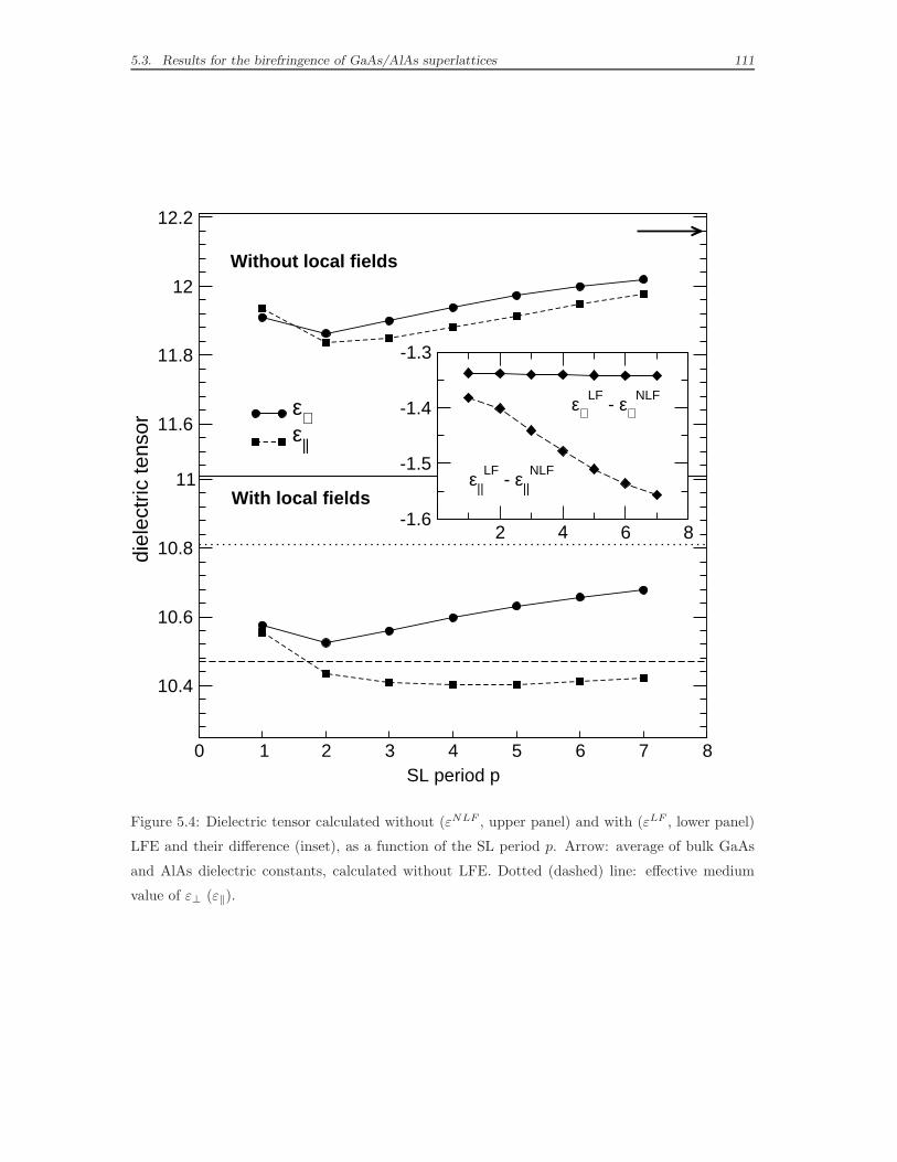
5.3. Results for the birefringence of GaAs/AlAs superlattices 111
0 1 2 3 4 5 6 7 8SL period p
10.4
10.6
10.8
11
diel
ectr
ic te
nsor
ε⊥ε||
11.6
11.8
12
12.2
Without local fields
With local fields
2 4 6 8-1.6
-1.5
-1.4
-1.3
ε⊥LF
- ε⊥NLF
ε||LF
- ε||NLF
Figure 5.4: Dielectric tensor calculated without (εNLF , upper panel) and with (εLF , lower panel)
LFE and their difference (inset), as a function of the SL period p. Arrow: average of bulk GaAs
and AlAs dielectric constants, calculated without LFE. Dotted (dashed) line: effective medium
value of ε⊥ (ε‖).

112 Chapter 5. Ab-initio calculations of optical properties
d depends only on |d| in a homogeneous medium, but it feels also its direction and
the absolute position of the charges when the medium is inhomogeneous. When d
is put in growth direction, the probability that the charges “see” where they are is
larger than when d is in-plane. Thus, local field effects are stronger on ε‖ than on
ε⊥. Last and most importantly, it remains to explain why local field effects increase
with increasing p in growth direction (see inset in Fig. 5.4), since it is finally this
fact which lets the birefringence tend to a plateau value instead of zero, as for large
superlattice period the lh and hh states are again degenerate. This point can in fact
be understood on the basis of the previous considerations: given a characteristic
interaction length |d| in the system, the bigger p the bigger is the probability that
the two charges are found either entirely in a region of GaAs or in a region of AlAs,
instead of experiencing a screening perfectly averaged over GaAs and AlAs.
All qualitatively observed tendencies can hence be explained. It remains to be
discussed what could be the origin of the remaining small quantitative discrepan-
cies with experiment. Besides possible uncertainties coming from the transmission
measurements, these might be sought on the theoretical side. Apart from various
approximations like the pseudopotential approach and the neglect of spin-orbit split-
ting, one might suspect, first, a contribution from the geometry of the system. In
fact, the band structure of bulk semiconductors has been shown to be very sensi-
tive to a small hydrostatic pressure [98]. This change in band structure could than
have significant effects on the dielectric properties. We have explored this possi-
bility by comparing the above results, obtained using the average theoretical LDA
lattice constant, with a calculation performed at the average experimental lattice
constant. The latter corresponds to a negative pressure of 20 kbar in the calcula-
tion. No improvement is obtained; rather, for p=5 the birefringence has increased
by 17%. There is hence some visible influence of the choice of the geometry in the
calculations on the results, and, although the most straightforward guess (i.e. the
ad hoc correction of the average LDA lattice constant) does not solve the problem,
we cannot exclude that a geometry closer to the exact (unknown) experimental one
might improve the situation. However, another point seems more crucial, namely,
the inclusion of exchange-correlation effects beyond the RPA. One can do this in
principle within the TDDFT scheme; in practice, calculations on realistic extended

5.3. Results for the birefringence of GaAs/AlAs superlattices 113
GaAs AlAs
EXP 10.9 8.2
semi-empirical without local fields 10.12 7.63
RPA without local fields 14.19 10.21
RPA with local fields 12.77 8.92
LDA with local fields 13.55 9.52
Table 5.1: Experimental [43] and calculated dielectric constants for the bulk GaAs and AlAs semi-
conductors. We report the results of semi-empirical calculations and RPA-TDDFT calculations,
both without local field effects, and the results of RPA-TDDFT and TDLDA calculations including
local field effects.
systems are at the best done using the TDLDA approximation. It is known that
the inclusion of the LDA xc kernel gives a minor contribution to optical absorption
spectra, but a (on the scale of our problem) significant effect on dielectric constants,
which might well change the birefringence. We have therefore checked this possi-
bility by adding the exchange-correlation effects within TDLDA. In Table 5.1 we
show all the calculated dielectric constants for GaAs and AlAs in comparison to
the experimental values [43]. When working within the TDLDA, the bulk dielectric
constants of both constituent materials increase as by much as 7 % [146]. However,
those changes cancel out in the birefringence, and both the plateau value as well
as the birefringence at intermediate distances remain virtually unchanged. This
does not necessarily imply that exchange-correlation effects are in fact negligible.
TDLDA is an approximation, and the fact that above we have related the bire-
fringence to the near-gap transitions of the optical spectra rises the suspicion that
only a theory which perfectly describes that region would be able to yield precise
quantitative values for the birefringence. Such an approach does today exist for
the ab initio calculation of optical properties, namely the simultaneous solution of
the self-energy Dyson equation and the Bethe-Salpeter equation describing excitonic
effects. It is of course out of reach at present to apply the full theory here.
In conclusion, concerning superlattice optical properties, we have calculated the
dielectric tensor and the static birefringence of GaAs/AlAs superlattices as a func-
tion of the superlattice period. The use of an effective medium theory to describe
114 Chapter 5. Ab-initio calculations of optical properties
the dielectric tensor is found to be justified in the growth direction. In the in-plane
direction, however, the direct effect of quantum confinement is large and a classical
theory fails. Having learned in the previous chapter that confinement and band-
mixing effects alone are not sufficient to reproduce the experimental data, we have
included local field effects in present calculations. We have pointed out that quan-
tum confinement effects are important to understand the fine structure of the optical
spectra even of relatively weakly confined systems like GaAs/AlAs, but that it is
completely insufficient to take them into account only via the band structure in an
independent-transition picture: local-field effects, which reflect the inhomogeneity of
the superlattice, effectively mix the formerly independent transitions and can there-
fore drastically enhance the anisotropy, up to a factor of 7 even for periods as small
as p = 8. Moreover, we have confirmed the results of previous semi-empirical calcu-
lations based on the independent-transition scheme, by performing ab-initio calcula-
tions in the same approximation (RPA without local fields). Only by including local
field effects experiments [16] can be interpreted even qualitatively. Further exchange-
correlation effects seem to cancel to a large extent on the anisotropy results, and can
therefore be neglected unless a fine quantitative analysis is required. Due to limita-
tions in the computational resources, at the moment a many-body Green’s function
approach, which fully account for electron-electron and electron-hole interaction is
out of reach. This fact calls for the search of an alternative approach to the problem
and makes particularly interesting the following section, in which we are presenting
an alternative way to account for many-body effects.
5.4 Effects of the long-range contribution to the xc kernel
on the bulk spectra
We move now to the problem absorption spectra up to 7 eV, for bulk GaAs and
AlAs systems. We want to discuss the effects of a static long-range contribution
−α/q2 to the xc kernel fxc of time dependent density functional theory. The time
dependent DFT approach still keeps the advantage of the static one to be compu-
tationally very efficient, and could in principle replace other successful, but more
cumbersome methods like the Bethe-Salpeter approach (BSE)[129, 147, 131, 132].

5.4. Effects of the long-range contribution to the xc kernel on the bulk spectra 115
However, there are two additional difficulties with respect to the case of static DFT:
(i) the approximate Vxc should now in principle not only be good enough to repro-
duce the ground state density and total energy, but the KS equation should also yield
eigenvalues close to the ones that would be obtained using the unknown exact Vxc
(not to be confused with the measurable quasi-particle energies) (ii) also the time-
dependent density variation of Vxc, i.e. the so-called xc kernel fxc = δVxc/δρ, has to
be well described. Here we will mainly deal with the problem (ii). It has turned out
that TDDFT yields good results using the local and adiabatic LDA approximation
(TDLDA) for the xc kernel fxc[128], provided that finite systems are considered.
Also electron energy loss spectra of solids are well described in TDLDA. However,
in both cases the main improvement with respect to the independent-particle KS
spectrum (i.e. with respect to a simple sum over independent transitions between
KS states) comes from the density variation of the Hartree potential (local field
effects in the solid) which is described exactly, and not from fxc. By the way of
contrast, the Hartree contribution is not sufficient to yield good absorption spectra
of solids, and taking into account fxc within TDLDA does not lead to a significant
(if at all) improvement [148]. Therefore, it would be extremely desirable to find a
better, generally applicable, fxc. Improvements might come through the inclusion of
dynamical (memory) effects and/or long-range nonlocal terms [128, 135]. Recently,
Reining et al. [30] have shown that a static long-range contribution (LRC) of the
form fxc(q,G,G′, ω) = −δG,G′α/|q + G|2 can simulate the strong continuum exci-
ton effect in the absorption spectrum of bulk Si (q is a vector in the first Brillouin
zone (BZ), G and G’ are reciprocal lattice vectors, and α is a material dependent
parameter). Here, we discuss the effects of such a contribution more in detail, by
considering also the real part of the dielectric function ε, for bulk GaAs and AlAs.
Analogous results for Si and other materials are discussed in Refs. [30] and [149].
We show that the real and imaginary parts of ε at low energy are extremely well
reproduced when just this long-range contribution is taken into account. It is pos-
sible to show [149] that the the approximation is not valid for the loss function, for
reasons which will be discussed. We also examine the dependence of the parameter
α on the material.
Before showing the results, we briefly review the origin of the long-range con-
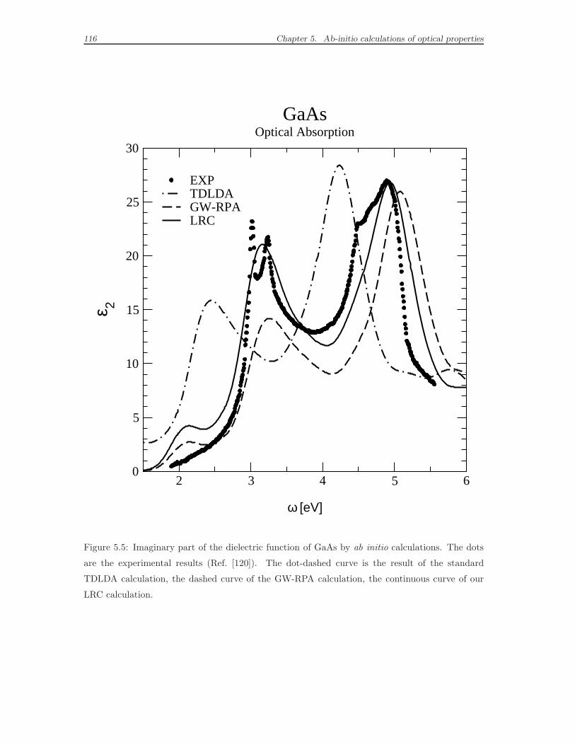
116 Chapter 5. Ab-initio calculations of optical properties
2 3 4 5 6
ω [eV]
0
5
10
15
20
25
30
ε 2
EXPTDLDAGW-RPALRC
GaAsOptical Absorption
Figure 5.5: Imaginary part of the dielectric function of GaAs by ab initio calculations. The dots
are the experimental results (Ref. [120]). The dot-dashed curve is the result of the standard
TDLDA calculation, the dashed curve of the GW-RPA calculation, the continuous curve of our
LRC calculation.

5.4. Effects of the long-range contribution to the xc kernel on the bulk spectra 117
tribution and its implementation. In TDDFT, the inverse dielectric function of a
periodic system is constructed from ε−1(q,G,G′) = δG,G′+v(q)Gχ(q,G,G′), where
χ obeys the matrix equation
χ = χ0 + χ0 (v + fxc)χ, (5.40)
χ0 being the independent-particle response function and v the bare Coulomb inter-
action. A similar equation can also be written for the macroscopic dielectric function
which describes absorption, namely εM(q,G,G′) = δG,G′ − v(q)Gχ(q,G,G′), with
χ = χ0 + χ0 (v + fxc) χ. (5.41)
Here, v(q)G equals v(q)G for all G, except for the long-range term v(q)(G=0) which
is zero. Both the equations for χ and for χ can be transformed to transition space,
as it is often done for χ in the framework of quantum chemistry [136]. This allows
a direct comparison to the BSE, for which this formulation is naturally adopted
[129, 147, 131, 132]. One finds then that a static fxc which yields the same spectrum
as the BSE should be of the form
fxc(q,G,G′) =
∑
n1n2n3n4
1
(fn1− fn2
)
Φ−1(n1, n2;G)F(n1n2)(n3n4)(Φ∗)−1(n3, n4;G
′), (5.42)
with
F(n1n2)(n3n4) =(
ǫQPn2
− ǫQPn1
− ǫDFTn2
+ ǫDFTn1
)
δn1n3δn2n4
+(fn1− fn2
)FBSE(n1n2)(n3n4) (5.43)
and
FBSE(n1n2)(n3n4) = −
∫
drdr′ Φ(n1, n3; r)W (r′, r)Φ∗(n2, n4; r′),
the matrices Φ being defined as
Φ(n1, n2; r) := ψn1(r)ψ∗
n2(r). (5.44)
Here, fn are occupation numbers and ǫDFT are KS eigenvalues. ǫQP are quasi-
particle (QP) eigenvalues, which are supposed to be calculated within Hedin’s GW
approach[96]. W is the statically screened Coulomb interaction, and the ψn are KS
118 Chapter 5. Ab-initio calculations of optical properties
orbitals, which are assumed to be equal to the QP ones. The matrices Φ can be
invertible if only a subspace of transitions is considered, which is actually the case for
absorption spectra. In a solid, the pairs of indices (n1, n2) are to be understood as a
pair of an occupied and an empty state, with (n1;n2) = (v,k; c,k+q). Φ(v,k, c,k+
q;G = 0) is going to zero as q for small q. Since F(v,c),(v,c) in this limit behaves
as a constant, this implies immediately that fxc(q,G = G′ = 0) behaves as 1/q2.
There is in fact a positive long-range contribution stemming from the QP shift of
eigenvalues (as also predicted in Ref. [152]), and a negative one resulting from the
electron-hole interaction, which is the main point of interest here.
Comparing Eqs. (5.40) and (5.41), one can understand why the long-range contri-
bution is much more important for absorption spectra than for the electron energy
loss spectra of solids: in the former case, in Eq. (5.41) fxc is added to a coulombian
v which does not contain the long-range term, i.e. v(G = 0) is set to zero. Obvi-
ously in that case, a neglect of the divergence in fxc makes an essential difference,
whereas in the case of loss spectra, determined via Eq. (5.40), this argument does
not hold. In order to focus the discussion about the long-range contribution on the
second, i.e. the electron-hole interaction contribution, we assume in the following
that we absorb the first, positive contribution in the energy shift of our starting
χ(0) (since anyway we do not know the eigenvalues of the exact exchange-correlation
potential which would go along with the exact kernel). Furthermore, we suppose
that we have a system where the long-range term is completely dominating the rest
of the exchange-correlation contribution, namely, where we can approximately write
fxc(q,G,G′) = −δG,G′α/|q + G|2. This long-range approximation for the screened
electron-hole interaction should of course work best for systems with weakly bound
excitons. This does not mean that the excitonic effects themselves are necessarily
weak, since the electron-hole interaction often drastically changes the spectral line-
shape, even when the joint density of states is not affected. In fact, we will consider
two materials that exhibit such a behavior, namely gallium arsenide and aluminum
arsenide. We have first determined their DFT-LDA electronic structure. Second,
we have constructed χ(0), but with the eigenvalues shifted to approximate GW ones,
in order to simulate the first part of the kernel as explained above. The GW eigen-
values are obtained by applying a scissor operator of 0.8 eV and 0.9 eV for GaAs
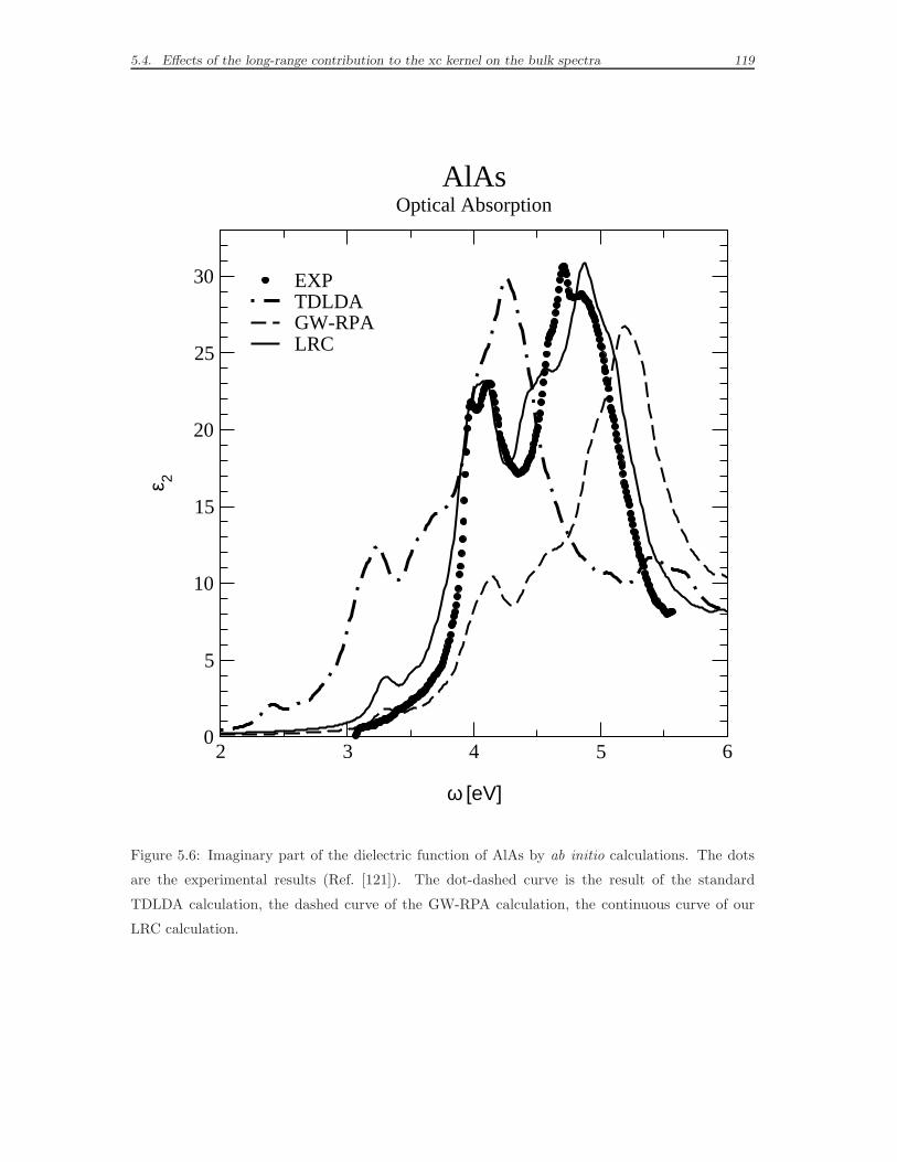
5.4. Effects of the long-range contribution to the xc kernel on the bulk spectra 119
2 3 4 5 6
ω [eV]
0
5
10
15
20
25
30
ε 2
EXPTDLDAGW-RPALRC
AlAsOptical Absorption
Figure 5.6: Imaginary part of the dielectric function of AlAs by ab initio calculations. The dots
are the experimental results (Ref. [121]). The dot-dashed curve is the result of the standard
TDLDA calculation, the dashed curve of the GW-RPA calculation, the continuous curve of our
LRC calculation.
120 Chapter 5. Ab-initio calculations of optical properties
and AlAs [86], respectively. Third, we have used fxc(r, r′) = −α/ (4π|r − r′|), with
an empirical value for α fitted to the experiment. The spectra have been obtained
using 864 off-symmetry shifted k-points in the Brillouin zone.
We are ready to discuss the results. Let us first look at absorption spectra.
Figs. 5.5 and 5.6 show the results for GaAs and AlAs. The dots are the experimental
results (Refs. [120] and [121], respectively). The dot-dashed curve stems from a
standard TDLDA calculation (i.e. using DFT-LDA eigenvalues and the static short-
range LDA xc kernel). Like other authors (see e.g. [148]), we find a result close to the
RPA one, showing the well-known discrepancies with experiment: peak positions are
wrong (the spectrum exhibits a redshift), and the intensity of the first main structure
(the E1 peak) is strongly underestimated. The dashed curve is the result obtained
by replacing KS eigenvalues with GW quasi-particle energies in the RPA form of ε.
This calculation, called GW-RPA in the following, corresponds to the first step of
our approach, as outlined above. Again, we find the well-known discrepancies with
experiment: now the calculated spectrum shows a blueshift. Moreover, the intensity
of the E1 structure has not been corrected. Finally, the continuous curve is the
result of our LRC calculation. For all three materials, a very good fit to experiment
is obtained using α = 0.2, 0.35 for GaAs and AlAs, respectively. One parameter is
hence enough for each of the materials in order to correct both the peak positions and
the intensities, which is far from trivial. Moreover, other features of ε are very well
reproduced using the same α, as we will discuss in the following. The next quantity
we can examine is in fact the real part of ε, Re(ε). Figs. 5.7 and 5.8 demonstrates the
failure to reproduce the experimental results (dots) of the RPA (continuous curve),
TDLDA (dot-dashed curve), and the GW-RPA (dashed curve) approaches. Again,
both peak positions and line shapes are wrong. Instead, the LCR result (continuous
curve) is compared to experiment: the improvement with respect to the GW-RPA
situation is clear, for both materials. Alternatively, a similar agreement of both real
and imaginary part of the dielectric function can only be found using the much more
cumbersome BSE approach (see e.g. [147, 131, 132, 150, 151]).
We have discussed the effects of a static long-range contribution −α/q2 to the
exchange-correlation kernel fxc of TDDFT. We have shown that the real and imag-
inary dielectric functions of GaAs and AlAs, exhibiting a strong continuum exciton
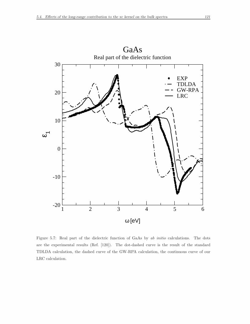
5.4. Effects of the long-range contribution to the xc kernel on the bulk spectra 121
1 2 3 4 5 6
ω [eV]
-20
-10
0
10
20
30
ε 1
EXPTDLDAGW-RPALRC
GaAsReal part of the dielectric function
Figure 5.7: Real part of the dielectric function of GaAs by ab initio calculations. The dots
are the experimental results (Ref. [120]). The dot-dashed curve is the result of the standard
TDLDA calculation, the dashed curve of the GW-RPA calculation, the continuous curve of our
LRC calculation.
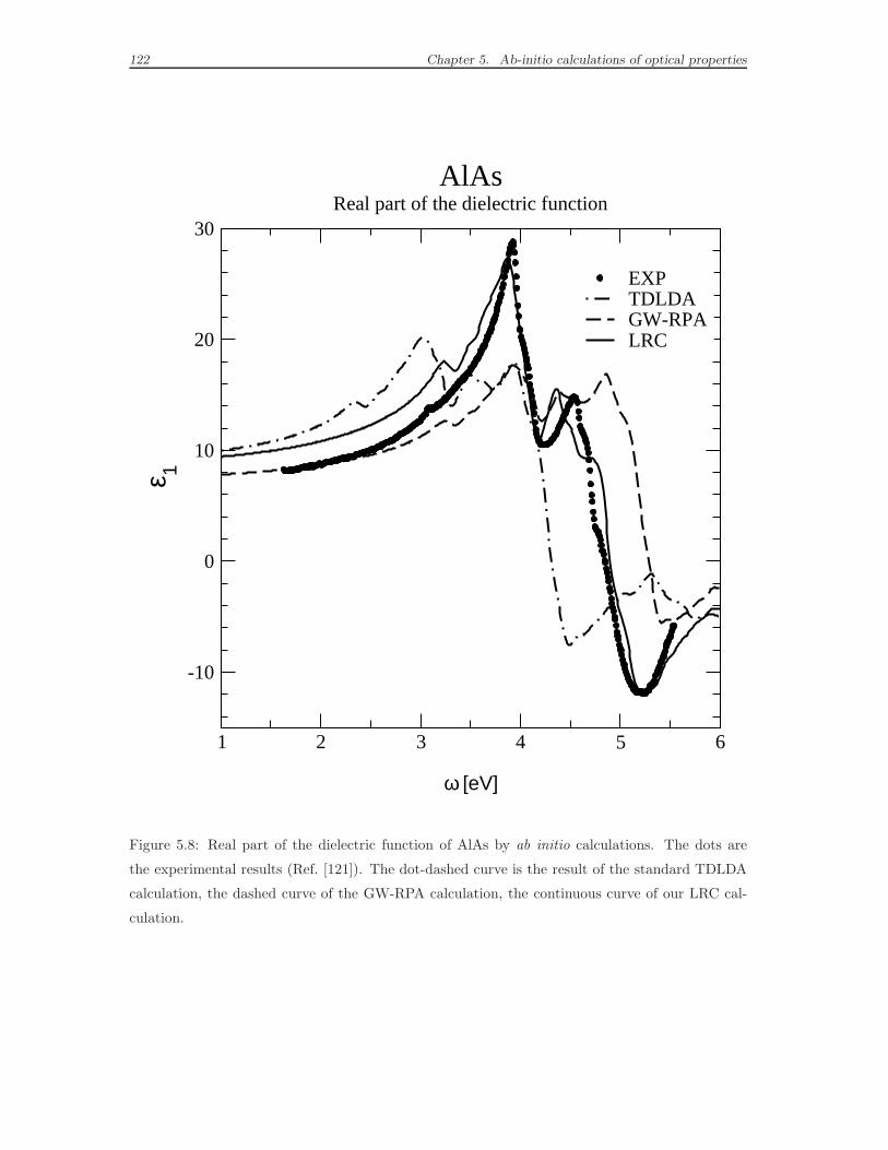
122 Chapter 5. Ab-initio calculations of optical properties
1 2 3 4 5 6
ω [eV]
-10
0
10
20
30
ε 1
EXPTDLDAGW-RPALRC
AlAsReal part of the dielectric function
Figure 5.8: Real part of the dielectric function of AlAs by ab initio calculations. The dots are
the experimental results (Ref. [121]). The dot-dashed curve is the result of the standard TDLDA
calculation, the dashed curve of the GW-RPA calculation, the continuous curve of our LRC cal-
culation.

5.4. Effects of the long-range contribution to the xc kernel on the bulk spectra 123
effect, are considerably improved with respect to calculations where the adiabatic local
density approximation is used. The findings allow to conclude that, for these ma-
terials, the problem of absorption spectra can be solved by just determining the one
number α. Of course, the method is neither valid for all kind of materials, nor for
all kind of excitation spectra. In spite of this, the good results for GaAs and AlAs en-
courage a future application of the theory to GaAs/AlAs superlattices, where it could
be an alternative to the too expensive many-body Green’s function formulation.

124 Chapter 5. Ab-initio calculations of optical properties
Chapter 6
Summary and discussion
Arriving at the end of this work, the easiest way to summarize the results achieved
is first to go back and read the four objectives presented in the introduction, to
follow then in this conclusive discussion how they have been developed in the course
of the chapters.
In Chapters 2 and 4, the energy bands and optical response functions of (001)-
oriented (GaAs)p/(AlAs)p and (GaAs)p/(vacuum)p superlattices, with p from 4 to
20, have been calculated by the LCBB method, introduced in Ref. [29]. This ap-
proach, in which the electronic states of the superlattice are expanded on the basis
of bulk states, calculated by empirical pseudopotentials, is found to be adequate
and practical for superlattices with intermediate to large periods; in particular, it is
useful for calculating how the band structures and the optical spectra of the bulk
materials are modified upon confinement.
In Chapter 2 we have studied the evolution of a bulk state into a superlattice
state, gaining a clear insight on the roles played by the confinement, the bulk states-
coupling and the reduction of the symmetry, all involved in the formation of a
superlattice. The bulk and superlattice band structures are very similar, nevertheless
there are some remarkable differences. The superlattice gaps are larger than the bulk
gaps: in particular the GaAs/vacuum gaps are larger than the GaAs/AlAs ones, as a
result of a stronger confinement; moreover the superlattice band gap widths increase
as the superlattice period decreases. The lowering in the crystal symmetry and the
mixing of the bulk states are responsible for the overall slight modification of the
125
126 Chapter 6. Summary and discussion
energy levels and, especially, for the removal of level degeneracies.
In Chapter 4 we have addressed the optical properties. The quantum-confinement
induced shifts of the critical point energies are calculated for both kinds of super-
lattices and are found to be larger for the GaAs/vacuum systems, where couplings
between different GaAs layers are only due to quantum-mechanical tunneling and
have a negligible effect. For both GaAs/AlAs and GaAs/vacuum superlattices,
the E1 peak in the absorption spectrum splits into two peaks with increasing blue
shifts for decreasing superlattice period. This result agrees with the observations
of Ref. [10] on GaAs/AlAs superlattices, and is attributed to a symmetry splitting
of the valence bands along the line Γ-L. The E2 transition is found to be split for
large-period GaAs/AlAs superlattices, where the electronic states of the bulk are
confined in each layer and the absorption spectrum is the superposition of the two
bulk ones. The energy of the E2 peak depends weakly on the superlattice period.
The average (or Penn) gap does not depend on the superlattice period, confirming
the expectation that a blue shift at the lower absorption edge is compensated by
red shifts in the upper part of the absorption spectrum. The band contribution
to linear birefringence of GaAs/AlAs superlattices is calculated and compared with
recent experimental results of Ref. [16]. The zero-frequency birefringence is found to
be much smaller than the experimental findings: this result hints that the missing
contribution to observed static birefringence may be attributed to local-field effects,
as already suggested [16]. The frequency-dependent part of the birefringence, arising
from band folding and quantum confinement, increases with decreasing superlattice
period, as found in the experiment, although the calculated values are smaller.
In Chapter 3 we have presented and applied the DFT-LDA to the calculation
of the ground state properties and the band structures of bulk GaAs and AlAs
systems and GaAs/AlAs superlattices. We have found an overall agreement with
corresponding semi-empirical results, and with experimental and theoretical data
available in literature. These findings confirm the analysis developed in Chapter 1
and attest the high quality of the electronic states, both semi-empirical and DFT-
LDA, which are the bases of the optical absorption calculations.
In Chapter 5 we have presented two different kinds of results. First, TDDFT cal-
culations of the dielectric tensor components and of the zero-frequency birefringence
127
of GaAs/AlAs superlattices as a function of the SL period, for p ranging from 1 to 8.
We have shown that the use of an effective medium theory is justified in the growth
direction for all periods but p=1. In the in-plane direction however, the dielectric
constant ε⊥ increases with increasing period, and the classical effective medium value
is reached to 90% for a period as small as p ≃ 10. We have pointed out that the
behavior of the dielectric tensor is completely determined by the interplay between
quantum confinement and local fields effects, and that the birefringence comes from
the anisotropy of the local fields. Quantum confinement effects are important to un-
derstand the fine structure of the optical spectra, even of relatively weakly confined
systems like GaAs/AlAs, but it is completely insufficient to take them into account
only via the band structure in an independent-transition picture: local-field effects,
which reflect the inhomogeneity of the superlattice, effectively mix the formerly in-
dependent transitions and can therefore drastically enhance the anisotropy, up to a
factor of 7 even for periods as small as p = 8. Including local field effects the ex-
periment [16] can be reproduced even quantitatively. Further exchange-correlation
effects seem to cancel to a large extent on the anisotropy results, and can therefore
be neglected unless a fine quantitative analysis is required. Then, we have shown
that, when working within the TDLDA, the bulk dielectric constants of both con-
stituent materials increase by as much as 7 %. However, those changes cancel out
in the birefringence, and both the plateau value as well as the birefringence at in-
termediate periods remain unchanged. In addition, we have confirmed the results
of previous semi-empirical calculations based on the independent-transition scheme,
for 6 ≤ p ≤ 8, by performing ab initio calculations in the same approximation.
Finally, we have presented a TDDFT calculation for bulk GaAs and AlAs, which
includes a static long-range contribution −α/q2 to the exchange-correlation kernel
fxc, as suggested by Reining et al. in Ref. [30]. We have shown that the real and
imaginary parts of the dielectric function, which exhibit strong continuum exciton
effects, are considerably improved with respect to calculations where the adiabatic
local density approximation is used. These findings allow to state that, for these
semiconductor systems, the problem of optical properties up to 10 eV could be solved
by just determining the one number α. This approach has the precious advantage
to reduce significantly the computation time and memory needed, in comparison
128 Chapter 6. Summary and discussion
to a many-body Green’s function approach. The good results for GaAs and AlAs
encourage a future application of the theory to GaAs/AlAs superlattices.
The present work can be extended in several other directions. Within the LCBB
scheme, relying on semi-empirical pseudopotentials, a more precise calculation of
the optical properties requires the inclusion of spin-orbit interaction and local-field
effects. On the other hand, a complete description of the E1 and E2 peaks requires,
in the semi-empirical framework as well, the inclusion of excitonic effects, which
account for half of the oscillator strength of the E1 transition in the bulk. Concern-
ing the ab initio approach, it is now possible to move to the study of other, more
complex, superlattice systems of technological interest or even to lower-dimensional
structures – quantum wires or quantum dots –, trying to clarify how the local field ef-
fects are modified and how they affect the anisotropy of the optical properties and/or
investigating the role of excitonic effects, including their effect on the anisotropy of
the optical response. This analysis could be applied to GaAs layers alternated with
an empty lattice, which are expected to show considerably stronger confinement
effects and can, in a first approach, simulate multilayer composites of GaAs and
oxidized-AlAs (GaAs/AlOx) [7]. Moreover, ZnSe/GaAs could be chosen as a repre-
sentative of heterovalent heterojunctions, in view of the good lattice match of the
two constituent materials, and in view of its potential technological importance as
a blue emitter [153]. Also Si/Ge is a system of technological interest, especially
since it has been discovered that short period (i.e. less than 20 interatomic dis-
tances) Si/Ge superlattices have a quasidirect band gap due to band folding, and
that the optical matrix elements between the top of the valence band and the new
band edge states at the center of the Brillouin zone are enhanced by several order
of magnitudes with respect to the ones for the lowest indirect transition, remaining
however at least one order of magnitude smaller than the optical matrix element
in a direct gap semiconductor such as GaAs [154]. Among the one-dimensional
systems in which anisotropy and excitonic effects should play an important role,
the study of silicon wires and gallium arsenide wires embedded in a matrix of alu-
minium arsenide is particularly promising. In fact, the first ones are important due
to their impact on the understanding of porous silicon [155], the latter ones for their
potential enhancement of the photovoltaic efficiency [156]. It would be interesting
129
to examine the possibility of matching the ab initio theory to the semi-empirical
method for superlattice periods larger than p = 8, to extrapolate ab initio results on
short/medium periods to qualitative or even semiquantitative predictions for larger
periods. Also one and zero-dimensional systems could be studied within this ap-
proach, which would be based on the introduction of a strongly reduced basis set,
given by the bulk DFT-LDA wavefunctions of the constituent materials, in analogy
with the LCBB scheme.

130 Chapter 6. Summary and discussion
Appendix A
Basic approximations
A solid is a many-body system (typically the number of degrees of freedom is of
the order of 1023), whose complete Hamiltonian consists in two terms depending
respectively on the space and spin coordinates of the nuclei Rα, i.e. VN−N , and on
the electronic space and spin coordinates ri, i.e. Ve−e, and a term of electron-nucleus
interaction, i.e. VN−e:
H = Te + TN + VN−N (Rα) + VN−e (ri,Rα) + Ve−e (ri) , (A.1)
where Te and TN represent the nuclear and electronic kinetic terms. Analytic solu-
tions of the Schrodinger equation are possible for a few extremely simple systems,
whereas numerical exact solutions can be calculated for a small number of atoms or
molecules. In the remaining cases, we have to introduce some simplifying hypotheses.
The development of schemes that provide some useful information on real systems
continues nowadays. Among the variety of possible choices, and hence of different
methods of calculations, the actual choice is intimately tied to the nature of the
problem of interest. The aim is to make the problem feasible, without invalidating
the physics of the results. We want to discuss here our specific approximations.
The inertia of a nucleus is much bigger than the inertia of an electron:
me ≪MN , (A.2)
in fact the mass ratio is equal to 1/2000 even in the most unfavorable case of the
hydrogen atom. From a classical point of view, the velocity of a nucleus is negligible
if compared to the velocity of an electron: we can state that an electron responds
131
132 Appendix A. Basic approximations
almost instantly to the motion of the nuclei or, the electrons see the nuclei as if they
were still. In the language of the quantum mechanics, this intuition becomes the
rigorous Born-Oppenheimer approximation: after rearranging the terms, in order to
isolate the electronic and ionic degrees of freedom, we write the wavefunction as a
product of an electronic part ψ (ri,Rα) and a nuclear part Φ (Rα). If we estimate
reasonable to neglect the term of interaction between the electrons and the lattice
motions (i.e. the electron-phonon interaction), we obtain a Schrodinger equation
where only the nuclear coordinates occur:
[HN + Ee (Rα)] Φ (Rα) = ET (Rα)Φ (Rα) . (A.3)
The presence of the electrons is included in the “adiabatic term” Ee (Rα), which
express the total energy of the electrons, in case the ion cores are “frozen” in the
positions Rα:
[Te (ri) + VN−e (ri,Rα) + Ve−e (ri)]ψ (ri,Rα) = Ee (Rα)ψ (ri,Rα) .(A.4)
In short, the problem can be reduced to two independent equations: first, Eq. (A.4)
describes the electrons when the ions are kept in a fixed set of positions, successively
Eq. (A.3) describes the lattice vibrations, considering that the ion cores feel the
electrons around them thanks to the adiabatic term. Concerning the system we are
interested in, the nuclei are finally located on the sites of a Bravais lattice. After the
separation has been put into effect, we can concentrate on the Eq. (A.4) regarding
the electronic degrees of freedom.
We will work within a pseudopotential framework (see Appendix B). When the
solid is built up, the electrons which belong to internal shells in the isolated atoms
(core electrons) remain strongly localized in the proximity of the nuclei, being almost
not affected by the chemical bonding. This is the physical motivation to separate
the core electrons from the valence electrons, by freezing them opportunely in the
core ions (core electrons + nuclei).
In spite of the previous approximations, the two-body electron-electron interac-
tion is still able to make the task formidable. We do not discuss here the big variety
of remedies studied to overcome this problem. In Chapters 2 an 3 we have presented
an empirical and a first-principle approach, which allow to reduce Eq. (A.4) to a
133
simpler effective one-particle band structure equation:
H1e φk,n(r) =( p2
2m+ V (r)
)
φk,n(r) = Ek,n φk,n(r) . (A.5)
In case of a periodic crystal, the solutions of Eq. (A.5) are Bloch functions
φk,n(r) = ei(k·r)un,k(r) , (A.6)
where un,k(r) has the periodicity of the Bravais lattice. The eigenstates are labelled
by the band indices n and the wavevector k, determined by the symmetry of the
lattice.

134 Appendix A. Basic approximations
Appendix B
Pseudopotentials
The concept of pseudopotentials was originally proposed in an early work of Fermi,
which dates back to 1934 [157]. In regard to solids, it was introduced as a variant
of the orthogonalized plane wave (OPW) method [158] and developed later in the
form of empirical pseudopotentials [159, 160]. In the 80’s the generalization from
empirical to ab initio norm-conserving pseudopotentials [161, 162, 163, 164] has
led to a widespread use of the method in calculations based on Density Functional
Theory (DFT), allowing empirical parameter free ground state property and band
structure calculations, where the only input data required are the atomic numbers
of the constituent atoms.
In this appendix we give an overview of the concept of pseudopotentials, both in
the empirical/semi-empirical and ab initio norm-conserving forms, and we discuss
their construction and their use.
B.1 What a pseudopotential is
When solving the many-body problem of electrons in a condensed aggregate of
atoms, a strong simplification consists in focusing on the charge density related to
electrons which belong to outermost shells (valence electrons). Many difficulties
come, in fact, from what happens in the inner region (core), but, fortunately, core
electrons are often not concerned in the bonding together of the atoms and can be
“frozen” once and for all in an atomic configuration, in order to restrict the effort
to the study of the valence electrons.
135
136 Appendix B. Pseudopotentials
The starting point is considering an isolated atom. An electron in the core region
feels roughly a Coulomb-like potential, −Zeff/r: the effective charge Zeff is given
by the positive nuclear charge, screened by the presence of the other electrons. An
highly attractive Coulomb term V implies, from the virial theorem
T = −1
2V , (B.1)
also a high positive kinetic energy T , which reflects a strong spatial variation of the
wavefunctions. This is true both for the core and the valence electrons, though the
valence electrons are far less likely to reach the neighborhood of the nucleus and
thus the amplitude of their oscillations is much smaller. Moreover, the waves have
to interlace in order to give wavefunctions which are orthogonal to each other.
Mathematically and numerically, a plane-wave-basis formalism is one of the sim-
plest and most natural formalism to implement in a computational code for crystals.
However, it is well known that a non-smooth character of the wavefunctions in the
real space correspond to a large number of plane waves to describe their Fourier
transforms. When using a plane wave representation for the wavefunctions, this is
a tough inconvenience, which results in a very high computational effort. A further
problem comes from the fact that the energy of the core states is of the order of
keV, while the relevant bonding energies are in the range of some eV: a high relative
precision for total energies is needed, even if only differences are of interest. The
introduction of pseudopotentials aims at finding a solution to these problems. In
fact, in many systems there is a clear separation between valence and core orbitals.
The core orbitals have energies far below the valence orbitals and their spatial extent
is limited. In this specific case the core does not react to changes in the chemical
environment and does not take part in the formation of bondings. But, in order to
forget about the core electrons, it is necessary to incorporate the effects due to their
presence in an effective potential, namely the pseudopotential, acting on the valence
electrons. This pseudopotential must be built in such a way to guarantee that the
solutions of the new Schrodinger equation have the same energy eigenvalues as the
solutions of the all-electron problem. However, unlike the all-electron wavefunctions,
the pseudowavefunctions should be smooth and nodeless. This is the essential nu-
merical constraint when building pseudopotentials; other requirements can be added
B.1. What a pseudopotential is 137
to give all the different recipes for the different types of pseudopotentials. In fact,
this is a problem whose solution is far from unique.
The core orbitals contribute to the Hartree and exchange-correlation potential
felt by the valence electrons with a repulsive potential, which comes from the fact
that each valence electron state ψ must be orthogonal to all the inner core electron
states ψc. We can write:
ψ = φ−∑
c
〈ψc|φ〉ψc , (B.2)
where we introduce the pseudowavefunction φ. Following Phillips and Kleinman
[158], substituting the Eq. ( B.2 ) into the the Schrodinger equation for the valence
electrons,
H ψ = E ψ , (B.3)
we obtain
(H + VR)φ = Eφ , (B.4)
where
VR =∑
c
(E − Ec) 〈ψc|φ〉ψc (B.5)
and Ec is the energy of the core state ψc:
H ψc = Ec ψc . (B.6)
The pseudopotential V PP can now be defined as the sum of the original long-range
attractive local potential VI , due to the Coulomb interaction with the core ions, and
the short-range repulsive potential VR just introduced, which is a memory of the
presence of the core states. The Eq. (B.4) is the wave equation for the pseudowave-
function φ. The resulting pseudopotential is weak and well-behaved, even inside the
core radius rc; this great simplification is obtained at the expense of introducing an
energy-dependent, non-local repulsive potential.
We can exploit the symmetry of the problem to expand the pseudopotential
V PP (r, r′) on a set of spherical harmonic functions: it is the non-locality which
leads to different components V PPl for the different angular momenta l. As all
components V PPl at large r reduce to the ionic Coulomb potential, −Zeff/r, getting
independent of l, it is intuitive to write the pseudopotential as the sum of a local
138 Appendix B. Pseudopotentials
potential V loc and a few relevant l-dependent terms which vanish beyond rc:
〈r|V PP |r′〉 = V locδ (r − r′) +lmax∑
l=0
l∑
m=−l
Y ∗lm (Ωr) δV
PPl (r)
δ (r − r′)
r2Ylm (Ωr′) , (B.7)
where
δV PPl = V PP
l − V loc (B.8)
and Ylm are spherical harmonics. Since the radial component δV PPl (r) is local, it is
more precise to call the whole pseudopotential “semi-local”, instead of non-local.
B.2 Empirical pseudopotentials
The pseudopotentials can be translated in suitable fitting functions, whose param-
eters can be easily determined starting from reflectivity or photoelectronic spectra:
this is the empirical pseudopotential method (EPM), which is by construction par-
ticularly suited to study optical properties. The pseudopotential has always the
periodicity of the Bravais lattice. Assuming cells of volume Ω, which contain Nα
atoms of type α, the local pseudopotential expansion as a Fourier series in the
reciprocal space has the form [9]:
V loc (r) =∑
G
vαGSαGeiG·r , (B.9)
where the G-vectors are the reciprocal lattice vectors,
vαG =1
Ω
∫
ΩV loc
α (r) e−iG·r dr (B.10)
is the pseudopotential form factor for the atom α and
SαG =1
Nα
Nα∑
j=1
e−iG·dα,j (B.11)
is the structure factor, depending on the position dα,j of the j-th atom of type α
in the primitive cell. The form factors are the fitting parameters. If we wish to
include the effects of non-locality we should write further correction terms in the
reciprocal space as a sum of l-dependent components. In the case of GaAs and
AlAs bulk crystals, the inclusion of non-local terms is needed to achieve a better
description of high-energy states: nevertheless, we have verified that only the low-
est conduction bands are responsible for the structures in the optical spectra below
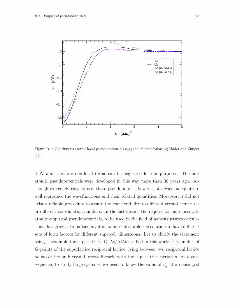
B.2. Empirical pseudopotentials 139
0 1 2 3 4 5
q (a.u.)
-0.5
-0.4
-0.3
-0.2
-0.1
0v
(e
V)
AlGaAs (in AlAs)As (in GaAs)
-1
α
Figure B.1: Continuous atomic local pseudopotentials vα(q) calculated following Mader and Zunger
[44].
6 eV and therefore non-local terms can be neglected for our purposes. The first
atomic pseudopotentials were developed in this way more than 30 years ago. Al-
though extremely easy to use, these pseudopotentials were not always adequate to
well reproduce the wavefunctions and their related quantities. Moreover, it did not
exist a reliable procedure to assure the transferability to different crystal structures
or different coordination numbers. In the last decade the request for more accurate
atomic empirical pseudopotentials, to be used in the field of nanostructures calcula-
tions, has grown. In particular, it is no more desirable the solution to have different
sets of form factors for different supercell dimensions. Let us clarify the statement
using as example the superlattices GaAs/AlAs studied in this work: the number of
G-points of the superlattice reciprocal lattice, lying between two reciprocal lattice
points of the bulk crystal, grows linearly with the superlattice period p. As a con-
sequence, to study large systems, we need to know the value of vαq at a dense grid
140 Appendix B. Pseudopotentials
of points q, which define the superlattice reciprocal lattice GSL. To this aim, it is
useful to develop a continuous-space empirical pseudopotential vα (q),
vα(q) =1
Ω
∫
Ωdr eiq·r vα(r) , (B.12)
to be used for all the possible different structures based on the same constituents,
including of course the bulk crystals (see Chapter 2). That is exactly what Zunger
et al. have done for different semiconductor compounds, starting from 1994 [44, 165,
166, 167, 168].
Concerning GaAs and AlAs crystals, we refer to the semi-empirical pseudopo-
tential functions proposed in Ref. [44]. We define them “semi-empirical” because
the fitting takes into account not only experiment, but also ab initio calculations.
The procedure adopted to evaluate the function (B.12) consists in the following
operations:
1. The origin of the zinc-blend primitive cell is fixed in the middle of the line
between the anion (As) and the cation (Ga or Al).
2. The bulk form factors vα(G) are adjusted at a small number of reciprocal lattice
vectors G to reproduce bulk band energies and effective masses. The operation
is repeated at different unit cell volumes Ω, to gain informations on the neigh-
borhood of each point G and dispose of a finer mesh which will make the inter-
polation less ambiguous. By inspecting the discrete form factors the algebraic
form selected for the fitting is a linear combination of Gaussians, multiplied by
a smooth function that allows adjustments of the small q components:
vα(q) =Ωα
Ω
4∑
i=1
aiα e−ciα(q−biα)2
[
1 + f0αe−βαq2
]
. (B.13)
3. At this stage the parameters of Eq. (B.13) are let free to vary independently
(the original form factors may change), to fit: (i) the experimental GaAs/AlAs
valence band offset (0.5 eV), (ii) LDA calculated level splittings in short-period
GaAs/AlAs superlattices of various orientations, (iii) first-principle LDA wave-
functions. In this way, it is possible to explore the region q < 2√
3πa
, where a is
the lattice constant: small q form factors are so fitted, rather than extrapolated.
Moreover, the above mentioned problem of previous empirical calculation which
yielded poor wavefunctions is finally solved.
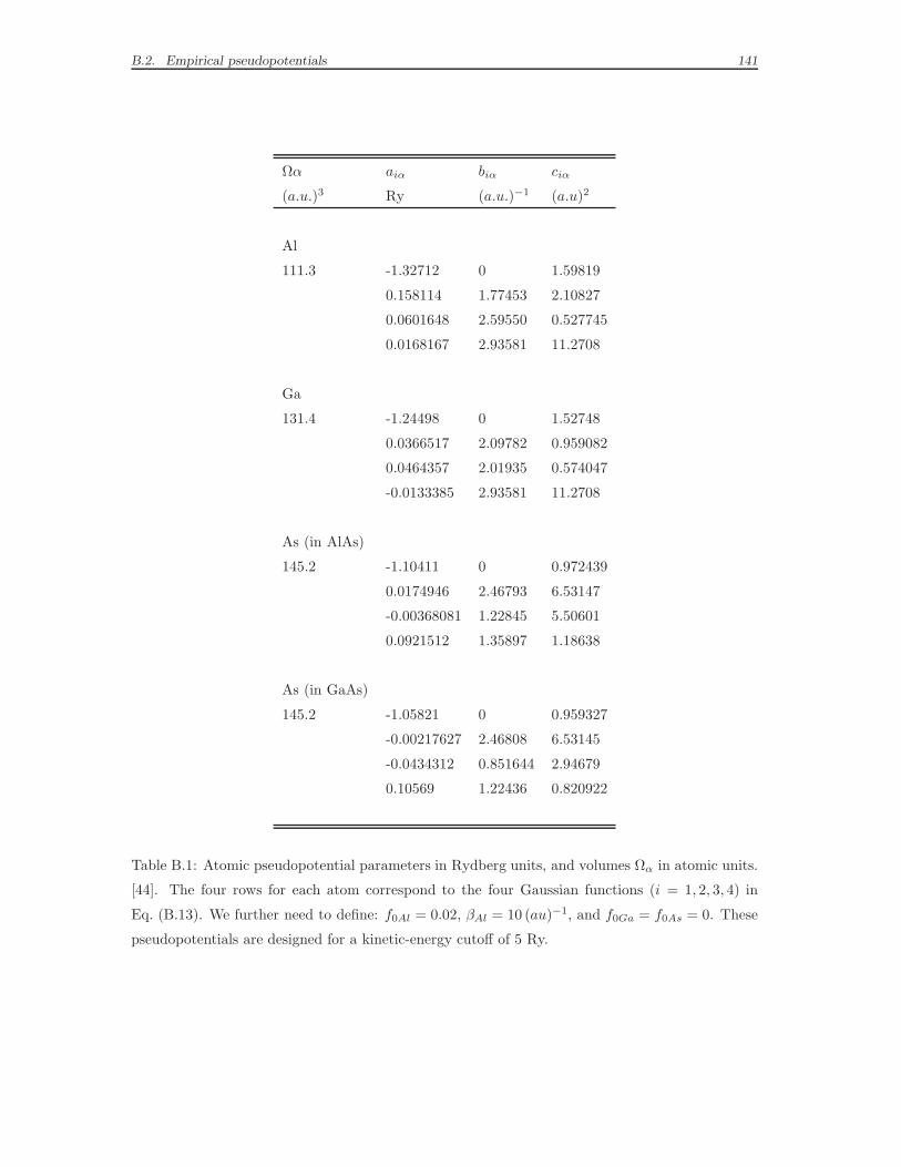
B.2. Empirical pseudopotentials 141
Ωα aiα biα ciα
(a.u.)3 Ry (a.u.)−1 (a.u)2
Al
111.3 -1.32712 0 1.59819
0.158114 1.77453 2.10827
0.0601648 2.59550 0.527745
0.0168167 2.93581 11.2708
Ga
131.4 -1.24498 0 1.52748
0.0366517 2.09782 0.959082
0.0464357 2.01935 0.574047
-0.0133385 2.93581 11.2708
As (in AlAs)
145.2 -1.10411 0 0.972439
0.0174946 2.46793 6.53147
-0.00368081 1.22845 5.50601
0.0921512 1.35897 1.18638
As (in GaAs)
145.2 -1.05821 0 0.959327
-0.00217627 2.46808 6.53145
-0.0434312 0.851644 2.94679
0.10569 1.22436 0.820922
Table B.1: Atomic pseudopotential parameters in Rydberg units, and volumes Ωα in atomic units.
[44]. The four rows for each atom correspond to the four Gaussian functions (i = 1, 2, 3, 4) in
Eq. (B.13). We further need to define: f0Al = 0.02, βAl = 10 (au)−1, and f0Ga = f0As = 0. These
pseudopotentials are designed for a kinetic-energy cutoff of 5 Ry.
142 Appendix B. Pseudopotentials
4. The As potential in GaAs and AlAs are not constrained to be identical, i.e. they
are fitted independently, to account for the local-environment dependence of the
atomic potential, by considering the local electronic charge. This is equivalent
to say that empirical/semi-empirical pseudopotentials are not transferable to
different chemical environments. The pseudopotential for As coordinated by n
Al atoms and (4 − n) Ga atoms is given by the weighted average:
vAs =n
4vAs (AlAs) +
4 − n
4vAs (GaAs) . (B.14)
This means that, to preserve a correct description of interfaces in GaAs/AlAs
superlattices, an As atom bound to two Al and two Ga atoms is attributed a
symmetrized pseudopotential, which is the average of the As pseudopotential
functions in GaAs and AlAs environments.
5. The quality of the final pseudopotentials is widely tested, in the contest of
plane-wave calculations in Ref. [44], in the contest of LCBB calculations in
Ref. [29].
These pseudopotentials are local and, at this stage, do not include spin-orbit terms,
even if in the Appendix of Ref. [44] it is suggested how to include them. Bulk and
superlattice energy levels are provided in the same absolute energy scale, thus su-
perlattice and bulk eigenvalues can be easily compared and the valence band offset
is automatically reproduced. The different q −→ 0 limit values of vα(q) are the
key-points to describe correctly the band alignment. The optimized parameters of
Eq. (B.13) are given in Table B.1. The energy cutoff these pseudopotentials are
designed for is 5 Ry. At last, we should add that the continuous pseudopotentials
presented here are not the only ones in literature. Nevertheless, trusting the compar-
ison table in Ref. [44], these pseudopotentials should be the more efficient, at least
for a superlattice constituted by GaAs and AlAs. Our results, both concerning the
bulk and superlattice systems, confirm the high quality of these pseudopotentials.
B.3. Ab-initio pseudopotentials 143
B.3 Ab-initio pseudopotentials
B.3.1 Hamann pseudopotentials
In a full DFT calculation, including explicitly both core and valence electrons, the
valence electrons feel potentials due to the nuclei, the core electrons and the other
valence electrons. The sum of the first two terms gives the true ionic potential.
Within a pseudopotential framework, the true ionic potentials are substituted by
the ionic pseudopotentials: the two potentials differ in a spherical region centered
on the nuclei. We can already underline a basic difference between this definition
of pseudopotentials and the semi-empirical pseudopotentials presented in the last
section: the semi-empirical pseudopotentials are screened, i.e. they include also
the effects due to the electron-electron interaction between valence electrons. This
explains, as we have already remarked, why empirical/semi-empirical pseudopoten-
tials cannot be transferable. In case of ionic pseudopotentials we do not meet this
restriction: it is practical to have a pseudopotential, which can be convenient to
describe the electronic properties in deeply different chemical environments, like an
excited atomic state, a molecule or a solid.
The formulation of modern ab initio pseudopotentials goes beyond the Phillips-
Kleinman scheme, overcoming some problems arising from the imperfect normaliza-
tion of the pseudowavefunction. In fact, if the true wavefunction ψ is normalized to
one, then from the (B.2):
1 = 〈φ|φ〉 − 2∑
c
〈ψc|φ〉〈φ|ψc〉 +∑
c
|〈ψc|φ〉 |2 ; (B.15)
it follows that the pseudowavefunction φ has a norm only approximatively equal to
one:
〈φ|φ〉 = 1 +∑
c
|〈ψc|φ〉 |2 . (B.16)
This is a consequence of the incorrect distribution of the valence charge between the
core and the valence region and would cause serious problems in self-consistent cal-
culations. This inconvenience is eliminated in the formulation of Hamann, Schluter
and Chiang [161], by imposing the conservation of the norm for the pseudowave-
function. In the framework of this formalism, Bachelet, Hamann and Schluter have
built systematically all the atomic norm-conserving pseudopotential from H to Pu

144 Appendix B. Pseudopotentials
[162]. This is not the only way to solve the problem, another possible way leads to
the soft non-norm-conserving pseudopotentials of Vanderbilt [169].
The construction of the Hamann pseudopotentials starts from an All-Electron
(AE) calculation, within density functional theory, for the isolated atom. The goal
is to build a soft potential without a singularity in the origin, nevertheless the new
potential must not change the physical properties of the system. The procedure can
be summarized in the following steps:
a) the Kohn-Sham equation for the radial part RAEnl of the atomic wavefunction
is solved self-consistently within an all-electron scheme:
−1
2
d2
dr2+l (l + 1)
2r2+ V AE [n; r]
r RAEnl (r) = ǫAE
nl r RAEnl (r) , (B.17)
where
V AE [n; r] = −Zr
+ VH [n; r] + V LDAxc (n(r)) , (B.18)
Z is the atomic number, VH [n; r] is the Hartree potential and V LDAxc (n(r)) is
the exchange-correlation potential in the local density approximation.
b) The all-electron radial wavefunctions RAEnl is modified, by making it smooth and
nodeless in the core region, to obtain the radial pseudowavefunction RPPnl . The
pseudowavefunction RPPnl must fulfill the pseudoatom Kohn-Sham equation,
−1
2
d2
dr2+l (l + 1)
2r2+ V PP
l [n; r]
r RPPnl (r) = ǫPP
nl r RPPnl (r) , (B.19)
To be more precise, the pseudowavefunctions RPPnl are built, under the con-
straint to fulfill the following requirements:
(i) For the same atomic configuration, the valence eigenvalues of the all-
electron Hamiltonian and the pseudo-Hamiltonian must be equal:
ǫAEnl = ǫPP
nl . (B.20)
(ii) The pseudowavefunction RPPnl (r) must coincide with RAE
nl (r) outside the
core region, i.e.
RAEnl (r) = RPP
nl (r) , (B.21)
for r beyond a cutoff distance called core radius rcl, which depends on the
angular momentum component l. The core radius rcl must include the
more external node of the l-th component of the all-electron wavefunction.
B.3. Ab-initio pseudopotentials 145
(iii) The integral∫ R
0
∣
∣
∣RAE,PPnl (r)
∣
∣
∣
2r2dr , (B.22)
with R > rcl, must give the same value for an all-electron wavefunction
and a pseudowavefunction: this relation expresses the conservation of the
norm. From the Eq. (B.22) it follows, thanks to the Gauss theorem, that
the electrostatic potential produced at distances r > rc by the pseudo-
charge distribution is equal to the potential produced by the true charge
distribution. The density functional theory is based on the concept of
charge density, thus it is fundamental to reproduce correctly the true charge
density of the system.
(iv) The logarithmic derivatives of the true wavefunction and the pseudowave-
function and their first derivatives with respect to the energy must converge
to the same values for R > rc:
1
RPPnl (r, ǫ)
dRPPnl (r, ǫ)
dr=
1
RAEnl (r, ǫ)
dRAEnl (r, ǫ)
dr. (B.23)
For a perfect pseudopotential Eq. (B.23) holds for every energy ǫ, not only
for the eigenvalues ǫnl. This equality comes from the theory of scattering
and, together with the point (iii), it is essential to guarantee the transfer-
ability of the atomic pseudopotential to different chemical environments.
The freedom left within the construction rules still allows to play with the
parameters to get a “soft” pseudopotential, i.e. a pseudopotential which leads
to a low cutoff energy for the plane-wave basis.
c) Once we have obtained the pseudowavefunction, the pseudopotential is ob-
tained by the inversion of the Eq. (B.19):
V PPscr,l (r) = ǫnl −
l (l + 1)
2r2+
1
2rRPPnl (r)
d2
dr2
[
rRPPnl (r)
]
. (B.24)
For a nodeless wavefunction the pseudopotential does not have any singular-
ity, except possibly at the origin, where it can be avoided by imposing the
wavefunction to be proportional to rl, when it is approaching the origin.
d) At this stage, the pseudopotential is screened, i.e. it contains the Hartree and
exchange-correlation potentials due to valence electrons. In this form, it is not
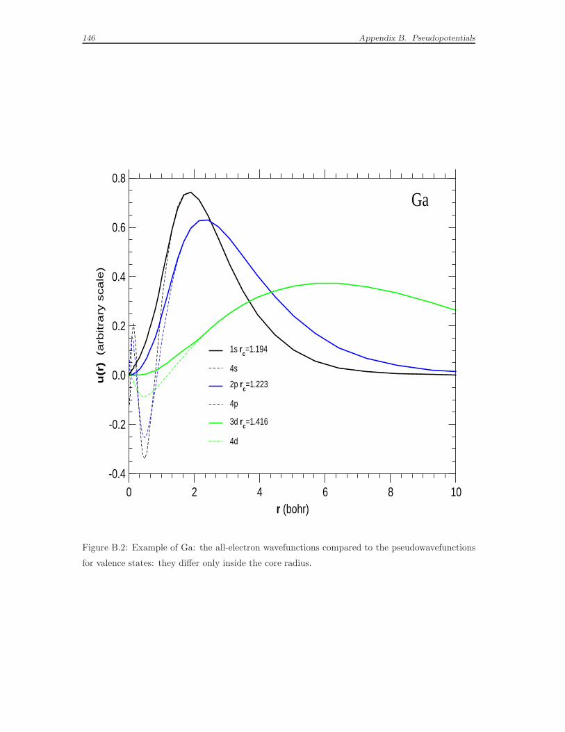
146 Appendix B. Pseudopotentials
0 2 4 6 8 10r (bohr)
-0.4
-0.2
0.0
0.2
0.4
0.6
0.8
u(r
) (
arb
itra
ry s
ca
le)
1s rc=1.194
4s
2p rc=1.223
4p
3d rc=1.416
4d
Ga
Figure B.2: Example of Ga: the all-electron wavefunctions compared to the pseudowavefunctions
for valence states: they differ only inside the core radius.
B.3. Ab-initio pseudopotentials 147
suitable to be used in a chemical environment which differs from the one in
which it has been generated. We need to remove the screening of the valence
electrons. Although the exchange-correlation energy is a non-linear functional
of the total electron density, in practice the “linearization” of the core-valence
contribution is usual and often adequate [170]. An explicit account of the
core-valence non-linearity of Vxc (non-linear core correction) [171] is sometimes
necessary, in particular if the overlap between the core and valence density is
remarkable. Anyway, whatever approximation has been chosen, the goal is to
subtract from the pseudopotential the contributions to the Hartree potential
and the exchange-correlation potential due to the valence electrons:
V PPion,l (r) = V PP
scr,l (r) − VH [nv; r] − Vxc [nv; r] . (B.25)
As a consequence of the process of construction of the “bare” pseudopotential,
we have a final result which depends explicitly on the components of the angular
momentum l :
V PPion (r, r′) =
∞∑
l=0
Plδ (r − r′)V PPion,l (r) , (B.26)
where Pl is the projector on the l-th eigenstate of the angular momentum. We
underline that the pseudopotential is local in the radial variables, but non-local
as far as angular coordinates are concerned: this kind of behavior characterized
a semi-local pseudopotential.
e) In the final formulation it is useful to separate a local long-range term from the
non-local short-range l-dependent terms:
V PPion (r, r′) := V PP
loc (r) + ∆V PPl (r, r′) = V PP
loc +inf∑
l=0
|l〉∆V PPl 〈l| . (B.27)
A typical choice is to set Vloc equal to one of the non-local components: the local
component can, in principle, be arbitrarily chosen, but since the summation in
Eq. (B.27) will need to be truncated at some value of l, the local potential should
be chosen such that it adequately reproduces the atomic scattering for all the
higher angular momentum channels. The maximum angular momentum lmax
depends both on the atom and on the electronic environment in which it lies. In
fact, in the solid the atomic electronic charge is redistributed and may be in an
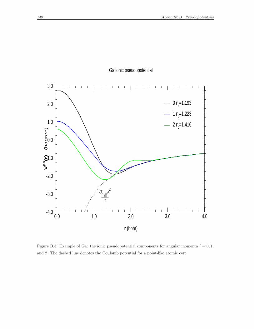
148 Appendix B. Pseudopotentials
0.0 1.0 2.0 3.0 4.0
r (bohr)
-4.0
-3.0
-2.0
-1.0
0.0
1.0
2.0
3.0
Vp
s(r
)
(hart
ree)
0 rc=1.193
1 rc=1.223
2 rc=1.416
Ga ionic pseudopotential
-Z eff
e2
r
Figure B.3: Example of Ga: the ionic pseudopotential components for angular momenta l = 0, 1,
and 2. The dashed line denotes the Coulomb potential for a point-like atomic core.
B.3. Ab-initio pseudopotentials 149
excited state if compared to the atomic ground state. For the construction of
excited angular momentum components it is necessary to rearrange the valence
charge into excited orbitals, maybe even in a ionic configuration. In Figs. B.3
and B.2 we show an example of the application of the Hamann scheme: the
non-local components of the pseudopotential of Ga are presented in Fig. B.3
on page 148, together with the ionic Coulomb potential. In Fig. B.2 on page
146 we show how the the wiggles in the valence states of Ga are eliminated,
moving from the real wavefunction to the pseudowavefunction.
The transferability and the smoothness of the pseudopotential are both strongly
affected by the choice of the core radius rcl. A high radius reduces the influ-
ence of the oscillating core states and brings to a softer pseudopotential, which
leads in its turn to a smaller energy cutoff of the plane-wave basis. On the
other hand, the transferability is lowered, due to the loss of physical relevant
information in the core region. For each atom the appropriate cutoff radius
must be selected as a compromise between fast convergence and good transfer-
ability. There are practical limits on how far rcl can be decreased: it must be
larger than the outermost node of the all-electron wavefunction; on the other
hand it must be small enough to prevent overlaps of neighboring core regions
when the molecule or the solid is created. Concerning the energy cutoff of the
plane wave basis, certain natural restrictions occur: the atomic size imposes
a length scale to the problem, which influences the extent of the Fourier ex-
pansion needed to accurately describe the pseudowavefunction. Anyway, a soft
pseudopotential prevents from wasting computational effort in unnecessarily
large expansions. The transferability depends critically also on the lineariza-
tion of the core-valence-exchange-correlation and, of course, on the choice of
the states to be included in the core. At last, another worsening to the trans-
ferability properties can come from the transformation of the pseudopotential
from the semi-local into the fully separable form. We will discuss this step in
a following section.
The comparison between the logarithmic derivative in an all-electron or pseu-
dopotential calculation, as already mentioned, gives clear hints on the transfer-
ability of the generated pseudopotentials. An additional quality requirement
150 Appendix B. Pseudopotentials
is the check that the all-electron atomic excitation or ionization energies and
the eigenvalues are close to the energy values obtained from the pseudopoten-
tial calculations and the all-electron frozen core calculations. According to this
test, a transferable pseudopotential should lead to the same accuracy as the
frozen-core all-electron calculation. Anyway, a final insight on the quality of
the pseudopotential can only be given by the results of realistic calculations on
different model systems (molecules or solids): the criterion is that a pseudopo-
tential and an all-electron calculation must deliver the same valence electronic
structure and the same total energy differences.
B.3.2 Troullier and Martins pseudopotentials
The prescriptions given in the previous section are not sufficient to define uniquely a
pseudopotential. It may be remarked that the smoothness of the pseudopotential has
never been explicitly required. It has been the objective of much active work trying
to determine some practical atomic criteria for a computational efficient pseudopo-
tential, which reproduces the correct all-electron behavior outside the core region.
Kerker [172] was the first to propose a pseudopotential construction which focused
on the smoothness of the pseudowavefunction. Troullier and Martins [163] gener-
alized and improved Kerker’s method, obtaining smooth pseudopotentials with a
relatively high cutoff radius, but still able to preserve good logarithmic derivatives.
Their recipe has proved to be particularly efficient for systems containing first row
elements, transition metals, and rare-earth elements. The first row elements, for
example, contain no p core electrons, thus their pseudopotential components with
p symmetry are very strong, because there are no inner p states to enforce the or-
thogonality. Transition metals and rare-earth elements have similar problems with d
and f components. Calculations involving atoms of the above type are particularly
demanding and these atoms provide an important test for pseudopotential smooth-
ness. The procedure of Troullier and Martins consists in modeling inside the core
radius the radial wavefunction in the form:
RPPnl (r) = rlepl(r2) , (B.28)
B.3. Ab-initio pseudopotentials 151
where pl is a polynomial of order six in r2. The seven variational coefficients of the
polynomial are chosen to fulfill the seven following conditions:
(i) Norm-conservation of charge within the core radius rcl, like in the Hamann
recipe.
(ii)-(vi) The continuity of the pseudopotential wavefunction and its first four deriva-
tives at rcl, which imposes in effect the continuity of V PPscr,l (r) and its first two
derivatives at rcl.
(vii) The zero curvature of the screened pseudopotential at the origin: V ′PPscr,l (0) = 0.
The last point is the criterion to give smooth pseudopotentials. This condition
has been accurately tested in Ref. [163]. Once the pseudowavefunction has been
defined, the procedure which leads to the pseudopotential is the standard method
described in the previous section. Although there are still no absolute criteria for
efficient pseudopotentials, the recipe by Troullier and Martins has been proven to
deliver excellent pseudopotentials, offering high transferability in combination with
fast convergence.
B.3.3 Kleinman-Bylander formulation
Working on a plane-wave representation entails performing some calculations in the
position space and some others in the momentum space, passing from one space to
the other thanks to a Fourier transform. In the reciprocal space the semi-local part
of the pseudopotential is described by the expression:
∑
G,G′
|k + G〉∆V PPl (k + G,k + G′) 〈k + G′| , (B.29)
which is completely non-local.
For an N -dimensional basis G , the semi-local form requires the evaluation and
storage of (N2+N)/2 matrix elements 〈k + G|∆V PPl |k + G′〉. Kleinman and Bylan-
der (KB) [173] found out that by complicating the expression of the pseudopotential
in real space, it is possible to save time and memory in their manipulation in recip-
rocal space. With the KB form the matrix elements of the non-local pseudopotential
between two states |k + G〉 and |k + G′〉 are expressed as the product of two fac-
tors, requiring only a number proportional to N of projections 〈∆V PPl φPP
lm |k + G〉

152 Appendix B. Pseudopotentials
and then simple multiplications. In fact, following Kleinman and Bylander, we can
rewrite in their separable form the non-local pseudopotential components:
∆V KBl =
∑
l,m
|∆V PPl φPP
lm 〉〈∆V PPl φPP
lm |〈φPP
lm |∆V PPl |φPP
lm 〉 , (B.30)
where φPPlm are the pseudoeigenfunctions of the Hamiltonian, obtained from the
semi-local atomic pseudopotential. The Fourier transform of Eq. (B.30) is:
∑
lm
[
∑
G |k + G〉〈k + G|∆V PPl φPP
lm 〉] [
∑
G′ 〈∆V PPl φPP
lm |k + G′〉〈k + G′|]
〈φPPlm |∆V PP
l |φPPlm 〉 . (B.31)
Of course, if we use the non-local part of the pseudopotential, as written in expres-
sion (B.30), to solve the electronic problem of the atom, we find the same eigenvalues
and eigenvectors we had already found with the pseudopotential expressed in the
semi-local form. This occurrence makes the KB pseudopotential in principle as valid
as the corresponding semi-local pseudopotential. Nevertheless, this procedure has
to be applied cautiously, because it can modify in a non-physical way the chemi-
cal properties of the atoms. The problem, as explained in Ref. [174], comes from
the fact that the KB Hamiltonian does not respect the Wronskian theorem [175].
According to the theorem, the atomic eigenfunctions are energetically ordered such
that, for a given quantum number l, the energies increase with the number of nodes.
Since this condition does not hold for the KB Hamiltonian, “ghost” states. i.e. un-
physical solutions, can show up in the chemically important energy range around
the valence eigenvalues El. There are some practical prescriptions to distinguish
and eliminate the ghost states : besides applying the criterion of Gonze et al. [174],
the logarithmic derivatives as a function of the energy must be accurately inspected,
comparing calculations using the all-electron Hamiltonian, the semi-local Hamilto-
nian and the KB Hamiltonian. If a ghost state is detected, occurring for some l,
it may be eliminated: (i) changing the component l which is set as the local part
of the potential, (ii) varying the core cutoff radii rcl of the l component or of the
local component. These changes should be done in such a way to preserve as good
as possible the transferability.

B.4. The norm-conserving pseudopotentials built to be used in this work 153
B.4 The norm-conserving pseudopotentials built to be used
in this work
In this section we want to discuss how we have applied the above explained tech-
niques to create norm-conserving pseudopotentials for Ga, As and Al atoms. The
tool used to perform the numerical calculation is the fhi98PP package [176] by
Fuchs and Scheffler. The code allows to generate norm-conserving pseudopoten-
tials adapted to DFT calculations, for all the interesting elements throughout the
periodic table. The procedure of construction is based on a scalar-relativistic all-
electron calculation of the free atom. Both the scheme by Hamann [177], described
in Section B.3.1, and the scheme by Troullier and Martins [163], described in Sec-
tion B.3.2, are implemented and can be selected by the user to generate the atomic
pseudopotentials. We remark once again that no experimental input is needed. The
exchange-correlation potential can be implemented both in different parameteriza-
tions of the local density approximation and in the generalized gradient approxi-
mation. A partial core density can be included to allow for non-linear core-valence
exchange-correlation. The package includes some facilities to test the quality of the
pseudopotentials directly on the free atom, in particular their softness and their
transferability, examining suitable cutoff energies for plane-wave basis set, scatter-
ing properties, excitation energies and chemical hardness properties. Moreover, the
presence of unphysical states, in case of Kleinman-Bylander separable pseudopoten-
tials, is detected by inspection of the bound spectrum and by the analysis of Gonze
et al. . For further details we suggest to see the Ref. [176].
Our ab initio pseudopotentials are generated using the method of Hamann et
al. [161] for Ga and As atoms, while the method of Troullier and Martins is used
for Al atoms. We have used the Kleinman-Bylander form for the pseudopotential,
after having accurately verified not to have ghost states. We have paid particular
attention to the choice of the reference configurations (see Table B.2), to mimic
as closely as possible the environment in which the atom is placed: this plays an
important role to assure a good description of the solid and, in particular, the lattice
mismatch between GaAs and AlAs. We remind that each atomic pseudopotential
is far from being unique and there are no fixed recipes to know a priori which
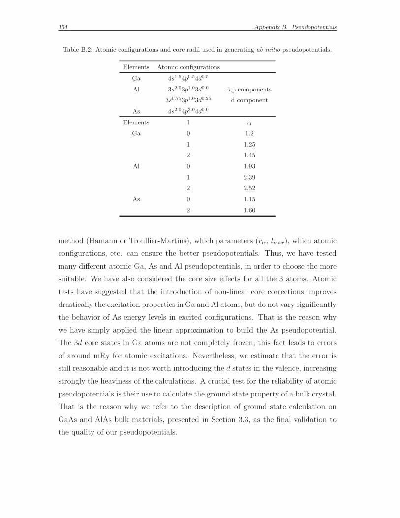
154 Appendix B. Pseudopotentials
Table B.2: Atomic configurations and core radii used in generating ab initio pseudopotentials.
Elements Atomic configurations
Ga 4s1.54p0.54d0.5
Al 3s2.03p1.03d0.0 s,p components
3s0.753p1.03d0.25 d component
As 4s2.04p3.04d0.0
Elements l rl
Ga 0 1.2
1 1.25
2 1.45
Al 0 1.93
1 2.39
2 2.52
As 0 1.15
2 1.60
method (Hamann or Troullier-Martins), which parameters (rlc, lmax), which atomic
configurations, etc. can ensure the better pseudopotentials. Thus, we have tested
many different atomic Ga, As and Al pseudopotentials, in order to choose the more
suitable. We have also considered the core size effects for all the 3 atoms. Atomic
tests have suggested that the introduction of non-linear core corrections improves
drastically the excitation properties in Ga and Al atoms, but do not vary significantly
the behavior of As energy levels in excited configurations. That is the reason why
we have simply applied the linear approximation to build the As pseudopotential.
The 3d core states in Ga atoms are not completely frozen, this fact leads to errors
of around mRy for atomic excitations. Nevertheless, we estimate that the error is
still reasonable and it is not worth introducing the d states in the valence, increasing
strongly the heaviness of the calculations. A crucial test for the reliability of atomic
pseudopotentials is their use to calculate the ground state property of a bulk crystal.
That is the reason why we refer to the description of ground state calculation on
GaAs and AlAs bulk materials, presented in Section 3.3, as the final validation to
the quality of our pseudopotentials.
Bibliography
[1] C. Weisbuch and B. Vinter, Quantum Semiconductor Structures (Academic
Press, San Diego, 1991).
[2] J. Singh, Physics of Semiconductors and their Heterostructures (McGraw-Hill,
New York, 1993).
[3] F. Capasso, J. Faist, and C. Sirtori, Physica Scripta T66, 57-59 (1996).
[4] Y.Y. Zhu and N.B. Ming, Optical and Quantum Electronics 31, 1093 (1999).
[5] D.C. Hutchings and B.S. Wherrett, Phys. Rev. B 52, 8150 (1995).
[6] K.J. Luo, S.W. Teitsworth, H. Kostial, H.T. Grahn, and N. Ohtani, Appl. Phys.
Lett. 70, 2825 (1997).
[7] A. Fiore, V. Berger, E. Rosencher, P. Bravetti, and J. Nagle, Nature 391, 463
(1998).
[8] M.L. Chelikowsky and J.R. Cohen, Electronic Structure and Optical Properties
of Semiconductors (Springer, Berlin, Heidelberg, 1989).
[9] P.Y. Yu and M. Cardona, Fundamentals of Semiconductors (Springer & Verlag,
Berlin, Heidelberg, 1996).
[10] M. Garriga, M. Cardona, N.E. Christensen, P. Lautenschlager, T. Isu, and
K. Ploog, Phys. Rev. B 36, 3254 (1987).
[11] M. Alouani, S. Gopalan, M. Garriga, and N.E. Christensen, Phys. Rev. Lett.
61, 1643 (1988).
[12] P. Tognini, L.C. Andreani, M. Geddo, and A. Stella, Phys. Rev. B 53, 6992
(1996).
155

156 Appendix B. Pseudopotentials
[13] C.W. Teng, J.F. Muth, R.M. Kolbas, K.M. Hassan, A.K. Sharma, A. Kvit, and
J. Narayan, Appl. Phys. Lett. 76, 43 (2000).
[14] G. Bastard, Wave Mechanics Applied to Semiconductor Heterostructures (Les
Editions de Physique, Paris, 1992).
[15] D. Kovalev, G. Polisski, J. Diener, H. Heckler, N. Kunzner, V. Yu Timoshenko,
and F. Koch, Appl. Phys. Lett. 78, 916 (2001).
[16] A.A. Sirenko, P. Etchegoin, A. Fainstein, K. Eberl, and M. Cardona, Phys. Rev.
B 60, 8253 (1999).
[17] O. Gunther, C. Janowitz, G. Jungk, B. Jenichen, R. Hey, L. Daweritz, and
K.P Loog, Phys. Rev. B 52, 2599 (1995).
[18] U. Schmid, N.E. Christensen, M. Cardona, F. Lukes, and K. Ploog, Phys. Rev.
B 45, 3546 (1992).
[19] K.B. Kahen and J.P. Leburton, Phys. Rev. B 33, 5465 (1986).
[20] J.B. Xia, Phys. Rev. B 38, 8358 (1988).
[21] R.G. Dandrea and A. Zunger, Phys. Rev. B 43, 8962 (1991).
[22] E. Ghahramani, D.J. Moss, and J.E. Sipe, Phys. Rev. B 43, 9269 (1991).
[23] Y.E. Kitaev, A.G. Panfilov, P. Tronc, and R.A. Evarestov, J. Phys. Cond. Mat.
9, 257 (1997).
[24] E. Herbert Li, J. Appl. Phys. 82, 6251 (1997).
[25] S.S. Li and B.F. Zhu, J. Phys. Cond. Mat. 10, 6311 (1998).
[26] J.-M. Gerard and B. Gayral, in Confined Photon Systems, edited by H. Benisty,
J.-M. Gerard, R. Houdre, J. Rarity, and C. Weisbuch (Springer, Berlin, 1999),
p. 331; J.-M. Gerard, private communication.
[27] D. Bergman, Physics Report 43, p. 291 (1978); M.G. Cottam and D.R. Tilley,
in Introduction to surface and superlattice excitations (Cambridge University
Press, Cambridge, 1989), p. 267; E. Jahne, Phys. Stat. Sol. (b) 194, 279 (1996).
B.4. The norm-conserving pseudopotentials built to be used in this work 157
[28] S. Botti and L.C. Andreani, Phys. Rev. B 63 , 235313 (2001).
[29] L.W. Wang, A. Franceschetti, and A. Zunger, Phys. Rev. Lett. 78, 2819 (1997).
[30] L. Reining, V. Olevano, A. Rubio, and G. Onida, submitted to Phys. Rev. Lett.,
cond-mat/0109434.
[31] L.W. Wang and A. Zunger, Phys. Rev. B 59, 15806 (1999).
[32] J.M. Luttinger and W. Kohn, Phys. Rev. 97, 869 (1955).
[33] E.O. Kane, J. Phys. Chem. Solids 1, 82-99 (1956); E.O. Kane, J. Phys. Chem.
Solids 1, 249 (1957).
[34] D.M. Wood and A. Zunger, Phys. Rev. B 53, 7949 (1996).
[35] L.W. Wang and A. Zunger, Phys. Rev. B 54, 11417 (1996).
[36] C. Pryor, Phys. Rev. B 57, 7190 (1998).
[37] H. Jiang and J. Singh, Phys. Rev. B 56, 4696 (1997).
[38] Y.T. Lu and L.J. Sham, Phys. Rev. B 40, 5567 (1989).
[39] H. Fujimoto, C. Hamaguchi, T. Nakazawa, K. Tauiguchi, K. Imanishi, H. Kato,
and Y. Watanabe, Phys. Rev. B 41, 7593 (1990).
[40] J.B. Xia and Y.C. Chang, Phys. Rev. B 42, 1781 (1990).
[41] Z.Q. Li and W. Potz, Phys. Rev. B 46, 2109 (1992).
[42] M.A. Gell and M. Jaros, Superlatt. Microstruct. 3, 121 (1987).
[43] L. Pavesi and M. Guzzi, J. Appl. Phys. 75, 4779 (1994).
[44] K.A. Mader and A. Zunger, Phys. Rev. B 50, 17393 (1994).
[45] S. Botti, “Laurea” thesis, Chapter 7, University of Pavia (1998).
[46] For a description of symmetry properties of superlattices see L.J. Sham and
Y.-T. Lu, J. Lumin. 44, 207 (1989).
[47] A. Franceschetti and A. Zunger, Phys. Rev. B 52, 14664 (1995); H. Fu and
A. Zunger, Phys. Rev. Lett. 80, 5397 (1998).
158 Appendix B. Pseudopotentials
[48] M. Hosoda, N. Ohtani, K. Tominaga, H. Mimura, and T. Watanabe, Phys. Rev.
B 56, 6432 (1997).
[49] G. Li, D. Jiang, H. Han, Z. Wang, and K. Ploog, Phys. Rev. B 40, 10430 (1989).
[50] L.H. Thomas, Camb. Philos. Soc. 23, 542 (1927).
[51] E. Fermi, Z. Phys. 48, 73 (1928).
[52] P. Hohenberg and W. Kohn, Phys. Rev. 136, B864 (1964).
[53] R.M. Dreizler and E.K.U. Gross, Density Functional Theory (Springer & Verlag,
Berlin, 1990).
[54] W. Kohn and L. Sham, Phys. Rev. 140, A1133 (1965).
[55] H. Englisch and R. Englisch, Phys. Stat. Sol. B 123, 711 (1984); H. Englisch
and R. Englisch, Phys. Stat. Sol. B 124, 373 (1984).
[56] D.M. Ceperley and B.J. Alder, Phys. Rev. Lett. 45, 566 (1980).
[57] J.P. Perdew and A. Zunger, Phys. Rev. B 23, 5084 (1981).
[58] J.P. Perdew, K. Burke, and Y. Wang Phys. Rev. B 54, 16533 (1996);
J.P. Perdew, K.A. Jackson, M.R. Pederson, D.J. Singh, and C. Fiolhais, Phys.
Rev. B 46, 6671 (1992).
[59] R.O. Jones and O. Gunnarsson, Rev. Mod. Phys. 61, 689 (1989).
[60] J.P. Perdew, Phys. Rev. Lett. 55, 1665 (1985); A.D. Becke, Phys. Rev. A 38,
3098 (1988); D.C. Langreth and M.J. Mehl, Phys. Rev. Lett. 47, 446 (1981);
J.P. Perdew, K. Burke, and M. Ernzerhof, Phys. Rev. Lett. 77, 3865 (1997).
[61] M. Fuchs, M. Bockstedte, E. Pehlke, and M. Scheffler, Phys. Rev. B 57, 2134
(1998), and references therein.
[62] O. Gunnarson, M. Johnson, and B.I. Lundqvist, Phys. Rev. B 20, 3136 (1979).
[63] A. Baldereschi, Phys. Rev. B 7, 5212 (1973).
[64] D.J. Chadi and M.L. Cohen, Phys. Rev. B 8, 5747 (1973).
B.4. The norm-conserving pseudopotentials built to be used in this work 159
[65] H.J. Monkhorst and J.D. Pack, Phys. Rev. B 13, 5188 (1976).
[66] O. Jepsen and O.K. Andersen, Phys. Rev. B 29, 5965 (1984).
[67] O. Jepsen and O.K. Andersen, Soldi State Commun. 9, 1763 (1971).
[68] G. Lehmann and M. Taut, Phys. Status Solidi B 54, 469 (1972).
[69] S. Baroni, A. Dal Corso, S. De Gironcoli, and P. Giannozzi,
http://www.pwscf.org.
[70] E.R. Davidson, Computer Phys. Commun. 53, 49 (1989).
[71] S.B. Zhang and M.L. Cohen, Phys. Rev. B 35, 7604 (1987).
[72] S.T. Weir, Y.K. Vohra, C.A. Vanderborgh, and A.L. Ruoff, Phys. Rev. B 39,
1280 (1989).
[73] N. Chetty, A. Munoz, and R.M. Martin, Phys. Rev. B 40, 11934 (1989).
[74] B.K. Agrawal and S. Agrawal, Phys. Rev. B 45, 8321 (1992).
[75] R.G. Greene, H. Luo, T. Li, and A.L. Ruoff, Phys. Rev. Lett. 72, 2045 (1994).
[76] G.C. Liu, Z.W. Lu, and B.M. Klein, Phys. Rev. B 51, 5678 (1995).
[77] A. Mujica, R.J. Needs, and A. Munoz, Phys. Rev. B 52, 8881 (1995).
[78] F.D. Murnaghan, Proc. Nat. Acad. Sci. USA 50, 697 (1944).
[79] F. Birch, J. Geophys. Res. 83, 1257 (1987).
[80] M. Levy, J.P. Perdew, and V. Sahni, Phys. Rev. A 30, 2745 (1984).
[81] P. Giannozzi, S. De Gironcoli, P. Pavone, and S. Baroni, Phys. Rev. B 43, 7232
(1991).
[82] A.L. Fetter and J.D. Walecka, Quantum Theory of Many-Particle Systems (Mc
Graw-Hill, New York, 1971).
[83] L. Hedin and S. Lundqvist, Solid State Physics, edited by F. Seitz, D. Turnbull,
and H. Ehrenreich (Academic, New York, 1969), Vol. 23, p.1.
[84] C.-O. Almbkadh and U. Von Bart, Phys. Rev. B 31, 3231 (1985).

160 Appendix B. Pseudopotentials
[85] M.S. Hybertsen and S.G. Louie, Phys. Rev. B 34, 5390 (1986).
[86] R.W. Godby, M. Schluter, and L.J. Sham, Phys. Rev. B 35, 4170 (1987).
[87] R.W. Godby, M. Schluter, and L.J. Sham, Phys. Rev. B 37 10159 (1988).
[88] M. Hybertsen and S.G. Louie, Phys. Rev. Lett. 55, 1418 (1985).
[89] M. Hybertsen and S.G. Louie, Phys. Rev. B 32, 7005 (1985).
[90] R.W. Godby, M. Schluter, and L.J. Sham, Phys. Rev. Lett. 56, 2415 (1986).
[91] R.W. Godby, M. Schluter, and L.J. Sham, Phys. Rev. B 36, 3497 (1987).
[92] L.J. Sham and M. Schluter, Phys. Rev. Lett. 51, 1888 (1983).
[93] J.P. Perdew and M. Levy, Phys. Rev. Lett. 51, 1884 (1983).
[94] M. Lannoo, M. Schluter, and L.J. Sham, Phys. Rev. B 32, 3890 (1985).
[95] L.J. Sham and M. Schluter, Phys. Rev. B 32, 3883 (1985).
[96] L. Hedin, Phys. Rev. B 139, 796 (1965).
[97] G.B. Bachelet and N.E. Christensen, Phys. Rev. B 31, 879 (1985).
[98] V. Fiorentini, Phys. Rev. B 46, 2086 (1992).
[99] Physics of Group IV Elements and III-V Compounds, edites by O. Madelung,
M. Schulz, and H. Weiss, Landolt-Bornstein, Numerical Data and Functional
Relationships in Science and Technology, New Series Group III, Vol. 17a
(Springer, New York, 1982).
[100] T.C. Chiang, J.A. Knapp, M. Aono, and D.E. Eastman, Phys. Rev. B 21,
3513 (1980).
[101] D.E. Aspnes, S.M. Kelso, R.A. Logan, and R. Bhatt, J. Appl. Phys. 60, 754
(1986).
[102] D.J. Wolford and J.A. Bradley, Solid State Commun. 53, 1069 (1985).
[103] D.E. Aspnes, C.G. Olson, and Q.W. Lynch, Phys. Rev. Lett. 37, 776 (1976).
B.4. The norm-conserving pseudopotentials built to be used in this work 161
[104] A. Onton, in Proceedings of the 10th International Conference on Physics of
Semiconductors, Cambridge, Massachusetts, 1970 (USAEC, New York, 1970),
p. 107.
[105] B. Monemar, Phys. Rev. B 8, 5711 (1973).
[106] D.M. Bylander and L. Kleinman, Phys. Rev. B 34, 5280 (1986).
[107] D.M. Wood, S.-H. Wei, and A. Zunger, Phys. Rev. B 37, 1342 (1988).
[108] B.I. Min, S. Massidda, and A.J. Freeman, Phys. Rev. B 38, 1970 (1988).
[109] S. Baroni, P. Giannozzi, and E. Molinari, Phys. Rev. B 41, 3870 (1990).
[110] F. Bassani and G. Pastori Parravicini, Electronic States and Optical Transi-
tions in Solids (Pergamon Press, Oxford, 1975).
[111] E.O. Kane, Phys. Rev. 180, 852 (1969).
[112] S. Antoci and G.F. Nardelli, Phys. Rev. B 6, 1311 (1972).
[113] V.M. Agranovich and V.E. Kravtsov, Solid State Commun. 55, 85 (1985).
[114] M. Cardona, in Semiconductor Superlattices and Interfaces, Proceedings of the
International School of Physics ”E. Fermi”, Course CXVII, edited by A. Stella
and L. Miglio (North-Holland, Amsterdam, 1993), p. 435.
[115] S.L. Adler, Phys. Rev. 126, 413 (1962).
[116] N. Wiser, Phys. Rev. 129, 62 (1963).
[117] W. Hanke, Advances in Physics 27, 287 (1978).
[118] V.U. Nazarov, Phys. Rev. B 49, 17342 (1994).
[119] G. Grosso and G. Pastori Parravicini, Solid State Physics (Academic Press,
London, 2000).
[120] P. Lautenschlager, M. Garriga, S. Logothetidis, and M. Cardona, Phys. Rev.
B 35, 9174 (1987).
[121] M. Garriga, M. Kelly, and K. Ploog, Thin Solid Films 233, 122 (1993).

162 Appendix B. Pseudopotentials
[122] S. Froyen, Phys. Rev. B 39, 3168 (1989).
[123] E.E. Mendez, L.L. Chang, G. Landgren, R. Ludeke, L. Esaki, and F.H. Pollak,
Phys. Rev. Lett. 46, 1230 (1981).
[124] See e.g. O. Krebs and P. Voisin, Phys. Rev. Lett. 77, 1829 (1996); O. Krebs,
P. Voisin, D. Rondi, J.L. Gentner, L. Goldstein, and J.C. Harmand, Physica E
2, 59 (1998).
[125] See e.g. J.D. Joannopoulos, R.D. Meade, and J.N. Winn, Photonic Crystals:
molding the flow of light (Princeton University Press, 1995).
[126] See e.g.: L.C. Andreani, Confined Electrons and Photons – new Physics and
Devices, edited by E. Burstein and C. Weisbuch (Plenum, New York, 1995), p.
57.
[127] E. Runge and E.K.U. Gross, Phys. Rev. Lett. 52, 997 (1984).
[128] E.K.U. Gross, F.J. Dobson, and M. Petersilka, Density Functional Theory
(Springer, New York, 1996).
[129] G. Onida, L. Reining, R.W. Godby, R. Del Sole, and W. Andreoni, Phys. Rev.
Lett. 75, 818 (1995); S. Albrecht, G. Onida, and L. Reining, Phys. Rev. B 55,
10278 (1997).
[130] S. Albrecht, L. Reining, R. Del Sole, and G. Onida, Phys. Rev. Lett. 80, 4510
(1998).
[131] L.X. Benedict, E.L. Shirley, and R.B. Bohn, Phys. Rev. B 57, R9385 (1998).
[132] M. Rohlfing and S.G. Louie, Phys. Rev. Lett. 81, 2312 (1998).
[133] E.K.U. Gross and W. Kohn, Phys. Rev. Lett. 55, 2850 (1985).
[134] E.K.U. Gross and W. Kohn, Phys. Rev. Lett. 57, 923 (1986).
[135] I.V. Tokatly and O. Pankratov, Phys. Rev. Lett. 86, 2078 (2001).
[136] see, e.g., M.E. Casida, in Recent Advances in Density Functional Methods,
Part I, edited by D.P. Chong (World Scientific, Singapore), p. 155.
B.4. The norm-conserving pseudopotentials built to be used in this work 163
[137] J. Dobson, G. Vignale, and M.P. Das, Electronic Density Functional Theory:
Recent Progress and New Directions (Plenum, New York, 1997).
[138] K. Burke, M. Petersilka, and E.K.U. Gross, Recent Advances in Density Func-
tional Methods, edited by P. Fantucci and A. Bencini (World Scientific, Singa-
pore, 2001).
[139] G. Onida, L. Reining, and A. Rubio, Rev. Mod. Phys., to be published.
[140] R. Van Leeuwen, Phys. Rev. Lett. 82, 3863 (1999).
[141] R. Del Sole and R. Girlanda, Phys. Rev. B 48, 11789 (1993).
[142] M. Cardona, in Atomic Structure and Properties of solids, edited by
E. Burstein (Academic Press, New york, 1972), P. 514.
[143] P. Etchegoin, A. Fainstein, A. Sirenko, B. Koopmans, B. Richards, P.V. San-
tos, M. Cardona, K. Totenmeyer, and K. Eberl, Phys. Rev. B 53, 13662 (1996).
[144] N. Vast, L. Reining, V. Olevano, P. Schattschneider, and B. Jouffrey, submit-
ted to Phys. Rev. Lett. .
[145] We found εGaAs and εAlAs, in agreement with previous calculations [81].
[146] M.S. Hybertsen and S.G. Louie, Phys. Rev. B 35, 5585 (1987).
[147] S. Albrecht, L. Reining, R. Del Sole, and G. Onida, Phys. Rev. Lett. 80, 4510
(1998).
[148] V.I. Gavrilenko and F. Bechstedt, Phys. Rev. B 55, 4343 (1997).
[149] S. Botti, V. Olevano, L. Reining, A. Rubio, and N. Vast, to be submitted.
[150] M. Rohlfing and S.G. Louie, Phys. Rev. B 62, 4927 (2000), and references
therein.
[151] B. Arnaud and M. Alouani, Phys. Rev. B 63, 085208 (2001).
[152] P. Ghosez, X. Gonze, and R.W. Godby, Phys. Rev. B 56, 12811 (1997).
[153] M.A. Haase et al., Appl. Phys. Lett. 59, 1272 (1991); H. Leon et al., Appl.
Phys. Lett. 59, 3619 (1991).
164 Appendix B. Pseudopotentials
[154] C. Tserbak and G. Theodorou, J. Appl. Phys. 76, 1062 (1994).
[155] see, e.g., L. Dorigoni, O. Bisi, F. Bernardini and S. Ossicini, Phys. Rev. B 53,
4557 (1996).
[156] A. Franceschetti and A. Zunger, Phys. Rev. B 52, 14664 (1995); M.H. Szy-
manska, P.B. Littlewood, and R.J. Needs Phys. Rev. B 63, 205317 (2001);
G. Goldoni, F. Rossi, E. Molinari, and A. Fasolino, Phys. Rev. B 55, 7110
(1997).
[157] E. Fermi, Il Nuovo Cimento 11, 157 (1934).
[158] J.C. Phillips and L. Kleinman, Phys. Rev. 116, 287 (1959).
[159] M.L. Cohen and V. Heine, Solid State Phys. 24, 37 (1970).
[160] J.R. Chelikowsky and M.L. Cohen, Phys. Rev. B 14, 556 (1976).
[161] D.R. Hamann, M. Schluter, and C. Chiang, Phys. Rev. Lett. 43, 1494 (1979).
[162] G. Bachelet, D.R. Hamann, and M. Schluter, Phys. Rev. B 26, 4199 (1982).
[163] N. Troullier and J.L. Martins, Phys. Rev. B 43, 1993 (1991).
[164] W.E. Pickett, Comments on Solid State Phys. 12, 57 (1986).
[165] L.W. Wang and A. Zunger, Phys. Rev. B 51, 17398 (1995).
[166] L. Bellaiche, S.H. Wei, and A. Zunger, Phys. Rev. B 54, 17568 (1996).
[167] H. Fu and A. Zunger, Phys. Rev. B 55, 1642 (1996).
[168] A.J. Williamson, J. Kim, L.W. Wang, S.-H. Wei, and A. Zunger cond-
mat/9805051.
[169] D. Vanderbilt, Phys. Rev. B 41, 7892 (1990).
[170] M. Fuchs, M. Bockstedte, E. Pehlke, and M. Scheffler, Phys. Rev. B 57, 2134
(1998).
[171] S.G. Louie, S. Froyen, M.L. Cohen, Phys. Rev. B 26, 1738 (1982).
[172] G.P. Kerker, J. Phys. C 13, L189 (1980).
B.4. The norm-conserving pseudopotentials built to be used in this work 165
[173] L. Kleinman and D.M. Bylander, Phys. Rev. Lett. 48, 1425 (1982).
[174] X. Gonze, R. Kackell, and M. Scheffler, Phys. Rev. B 41, 12264 (1990);
X. Gonze, P. Kackell, and M. Scheffler, Phys. Rev. B 41, 12264 (1990).
[175] A. Messiah, Quantum Mechanics (North-Holland, Amsterdam, 1974), Vol. 1,
p. 98.
[176] M. Fuchs and M. Scheffler, Computer Physics Communications.
[177] D.R. Hamann, Phys. Rev. B 40, 2980 (1989).

Ringraziamenti
E giunto il momento di scrivere di nuovo la parola fine. Inevitabilmente, i ringrazi-
amenti diventano l’occasione per tirare le somme di questi anni di dottorato, 3 anni
passati tra Pavia e Parigi. Mi sono accorta, prima con disappunto, poi riflettendoci
con piacere, che gli amici “pavesi e parigini” sono tanto numerosi da rendere impossi-
bile ringraziarli singolarmente. Questo punto da solo e gia sufficiente a rendere il mio
personale bilancio molto positivo. Ma c’e di piu. Penso che il dottorato non sia stato
un “parcheggio”, come molti di noi temevano al momento di decidere cosa fare dopo
la laurea. E stato un’esperienza formativa che mi ha molto arricchito, indipendente-
mente da quello che faro a partire da domani. A questo proposito voglio ringraziare
tutte le persone con cui ho avuto l’opportunita di collaborare. Primi fra tutti, il mio
tutore Claudio Andreani a Pavia, insieme a Lucia Reining, Nathalie Vast e Valerio
Olevano a Parigi. Grazie ad Angel Rubio per le interessanti discussioni. Lavorare
con loro e stato e spero continui a essere un grande privilegio. Grazie ad Alberto per
aver curato la preparazione dei miei seminari in francese e per la lettura critica della
mia tesi. Grazie a Roberto per essersi occupato delle noiose questioni burocratiche
a Pavia e della fase di stampa. Grazie a Francesco e Mario per i frequenti aiuti in
campo informatico. La correzione attenta del manoscritto a cui Lucia e Nathalie
hanno dedicato il loro gia esiguo tempo libero e stata un aiuto insostituibile. Voglio
inoltre ringraziare per la sua disponibilita Rodolfo Del Sole, lettore della mia tesi.
Dei ringraziamenti particolari vanno a Sergio Ratti, Coordinatore del Dottorato in
Fisica a Pavia, e a Guillaume Petite, Direttore del Laboratoire des Solides Irradies,
per l’accoglienza straordinaria che mi ha riservato. Un grazie sentito, inoltre, a tutti
i colleghi/amici del Gruppo di Teoria dello Stato Solido e del gruppo NMR a Pavia
e del Laboratoire des Solides Irradies a Palaiseau, per aver reso sempre piacevole il
tempo lavorativo e non lavorativo passato insieme. Infine, grazie a tutti gli amici,
vecchi e nuovi, e alla mia famiglia, con cui ho condiviso quotidianamente questa
esperienza. Non prendetevela se non vi nomino a uno a uno, avete tutti un posto
speciale.
FINE


![flogosi [modalità compatibilità] - UniFI · floggg )ogeno) • Flogosi cronica ab initio. ISTOFLOGOSI II • Fenomeni vascoloFenomeni vascolo--essudativi scarsiessudativi scarsi](https://static.fdocumenti.com/doc/165x107/5f0e24a97e708231d43dd168/flogosi-modalit-compatibilit-unifi-floggg-ogeno-a-flogosi-cronica-ab.jpg)


![Dinamica molecolare ab initio molecular dynamics of imidazole in … · Poichè la teoria di Hartree-Fock sottostima la correlazione elettronica[7, 11, 12, 13], non si ottiene un'accurata](https://static.fdocumenti.com/doc/165x107/5c6ab30409d3f20f298cfe95/dinamica-molecolare-ab-initio-molecular-dynamics-of-imidazole-in-poiche-la.jpg)