Generatore di clock mediante NE 555 - antoniosantoro.com terza pdf... · Generatore di clock...
53
Generatore di clock mediante NE 555.doc | rev. 1 del 25/06/2008 pagina 1 di 13 1 Generatore di clock mediante NE 555 Consideriamo la seguente figura VCC 1 2 Q1 3 2 1 5 K 5 K 5 K + - + - C1 R S CL Q R1 R2 10 nF 5 6 8 4 7 3 1 2 B A L’integrato NE555 è rappresentato dalla parte racchiusa dalla linea tratteggiata. I numeri presenti in prossimità di tale linea individuano i pin dell’integrato. Si nota, all’interno dell’integrato, un latch di tipo SR. Un latch di tipo SR è un circuito sequenziale con due ingressi denominati S ed R e due uscite Q e Q che soddisfano la seguente tabella
Transcript of Generatore di clock mediante NE 555 - antoniosantoro.com terza pdf... · Generatore di clock...

Generatore di clock mediante NE 555.doc | rev. 1 del 25/06/2008 pagina 1 di 13
1
Generatore di clock mediante NE 555
Consideriamo la seguente figura
VCC
1 2
Q13
21
5 K
5 K
5 K
+
-
+
-
C1
R
S
CL Q
R1
R2
10 nF
5
6
8 4 7
3
1
2
B
A
L’integrato NE555 è rappresentato dalla parte racchiusa dalla linea
tratteggiata. I numeri presenti in prossimità di tale linea individuano i pin
dell’integrato. Si nota, all’interno dell’integrato, un latch di tipo SR. Un latch
di tipo SR è un circuito sequenziale con due ingressi denominati S ed R e due
uscite Q e Q che soddisfano la seguente tabella
Generatore di clock mediante NE 555.doc | rev. 1 del 25/06/2008 pagina 2 di 13
2
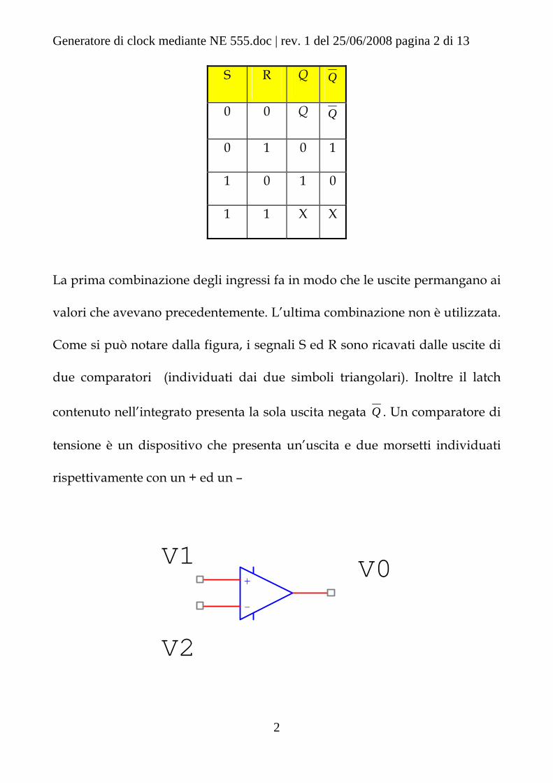
S R Q Q
0 0 Q Q
0 1 0 1
1 0 1 0
1 1 X X
La prima combinazione degli ingressi fa in modo che le uscite permangano ai
valori che avevano precedentemente. L’ultima combinazione non è utilizzata.
Come si può notare dalla figura, i segnali S ed R sono ricavati dalle uscite di
due comparatori (individuati dai due simboli triangolari). Inoltre il latch
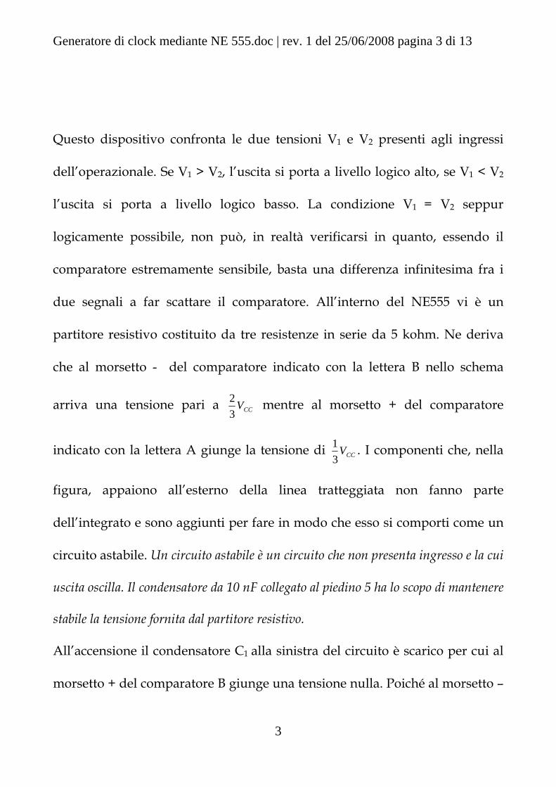
contenuto nell’integrato presenta la sola uscita negata Q . Un comparatore di
tensione è un dispositivo che presenta un’uscita e due morsetti individuati
rispettivamente con un + ed un –
+
-
V1
V2
V0
Generatore di clock mediante NE 555.doc | rev. 1 del 25/06/2008 pagina 3 di 13
3
Questo dispositivo confronta le due tensioni V1 e V2 presenti agli ingressi
dell’operazionale. Se V1 > V2, l’uscita si porta a livello logico alto, se V1 < V2
l’uscita si porta a livello logico basso. La condizione V1 = V2 seppur
logicamente possibile, non può, in realtà verificarsi in quanto, essendo il
comparatore estremamente sensibile, basta una differenza infinitesima fra i
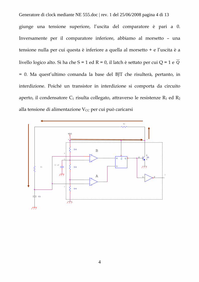
due segnali a far scattare il comparatore. All’interno del NE555 vi è un
partitore resistivo costituito da tre resistenze in serie da 5 kohm. Ne deriva
che al morsetto - del comparatore indicato con la lettera B nello schema
arriva una tensione pari a CCV32 mentre al morsetto + del comparatore
indicato con la lettera A giunge la tensione di CCV31 . I componenti che, nella
figura, appaiono all’esterno della linea tratteggiata non fanno parte
dell’integrato e sono aggiunti per fare in modo che esso si comporti come un
circuito astabile. Un circuito astabile è un circuito che non presenta ingresso e la cui
uscita oscilla. Il condensatore da 10 nF collegato al piedino 5 ha lo scopo di mantenere
stabile la tensione fornita dal partitore resistivo.
All’accensione il condensatore C1 alla sinistra del circuito è scarico per cui al
morsetto + del comparatore B giunge una tensione nulla. Poiché al morsetto –
Generatore di clock mediante NE 555.doc | rev. 1 del 25/06/2008 pagina 4 di 13
4
giunge una tensione superiore, l’uscita del comparatore è pari a 0.
Inversamente per il comparatore inferiore, abbiamo al morsetto – una
tensione nulla per cui questa è inferiore a quella al morsetto + e l’uscita è a
livello logico alto. Si ha che S = 1 ed R = 0, il latch è settato per cui Q = 1 e Q
= 0. Ma quest’ultimo comanda la base del BJT che risulterà, pertanto, in
interdizione. Poiché un transistor in interdizione si comporta da circuito
aperto, il condensatore C1 risulta collegato, attraverso le resistenze R1 ed R2
alla tensione di alimentazione VCC per cui può caricarsi
VCC
1 2
Q13
21
5 K
5 K
5 K
+
-
+
-
C1
R
S
CL Q
R1
R2
10 nF
5
6
8 4 7
3
1
2
B
A
Generatore di clock mediante NE 555.doc | rev. 1 del 25/06/2008 pagina 5 di 13
5
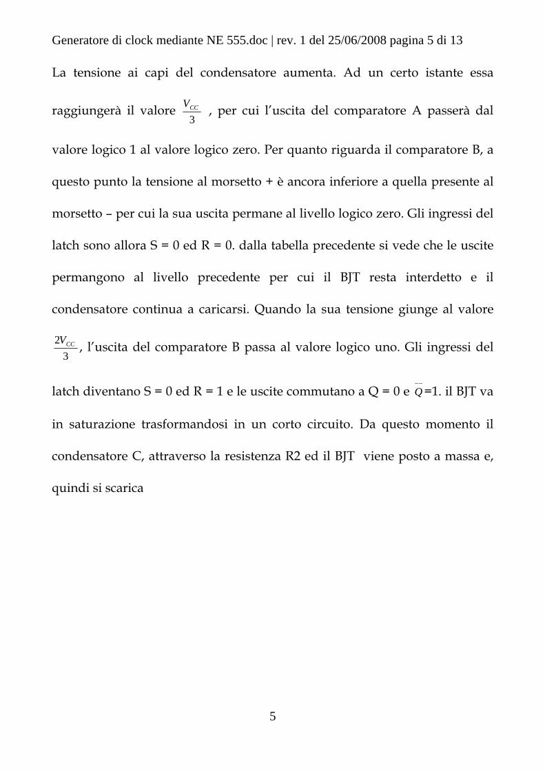
La tensione ai capi del condensatore aumenta. Ad un certo istante essa
raggiungerà il valore 3CCV , per cui l’uscita del comparatore A passerà dal
valore logico 1 al valore logico zero. Per quanto riguarda il comparatore B, a
questo punto la tensione al morsetto + è ancora inferiore a quella presente al
morsetto – per cui la sua uscita permane al livello logico zero. Gli ingressi del
latch sono allora S = 0 ed R = 0. dalla tabella precedente si vede che le uscite
permangono al livello precedente per cui il BJT resta interdetto e il
condensatore continua a caricarsi. Quando la sua tensione giunge al valore
32 CCV , l’uscita del comparatore B passa al valore logico uno. Gli ingressi del
latch diventano S = 0 ed R = 1 e le uscite commutano a Q = 0 e −−
Q =1. il BJT va
in saturazione trasformandosi in un corto circuito. Da questo momento il
condensatore C, attraverso la resistenza R2 ed il BJT viene posto a massa e,
quindi si scarica
Generatore di clock mediante NE 555.doc | rev. 1 del 25/06/2008 pagina 6 di 13
6
VCC
1 2
Q13
21
5 K
5 K
5 K
+
-
+
-
C1
R
S
CL Q
R1
R2
10 nF
5
6
8 4 7
3
1
2
B
A
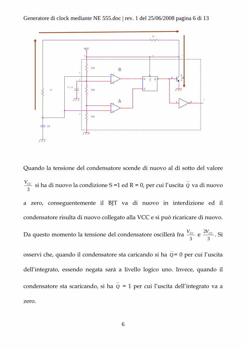
Quando la tensione del condensatore scende di nuovo al di sotto del valore
3CCV si ha di nuovo la condizione S =1 ed R = 0, per cui l’uscita
−−
Q va di nuovo
a zero, conseguentemente il BJT va di nuovo in interdizione ed il
condensatore risulta di nuovo collegato alla VCC e si può ricaricare di nuovo.
Da questo momento la tensione del condensatore oscillerà fra 3CCV e
32 CCV . Si
osservi che, quando il condensatore sta caricando si ha −−
Q = 0 per cui l’uscita
dell’integrato, essendo negata sarà a livello logico uno. Invece, quando il
condensatore sta scaricando, si ha −−
Q = 1 per cui l’uscita dell’integrato va a
zero.
Generatore di clock mediante NE 555.doc | rev. 1 del 25/06/2008 pagina 7 di 13
7
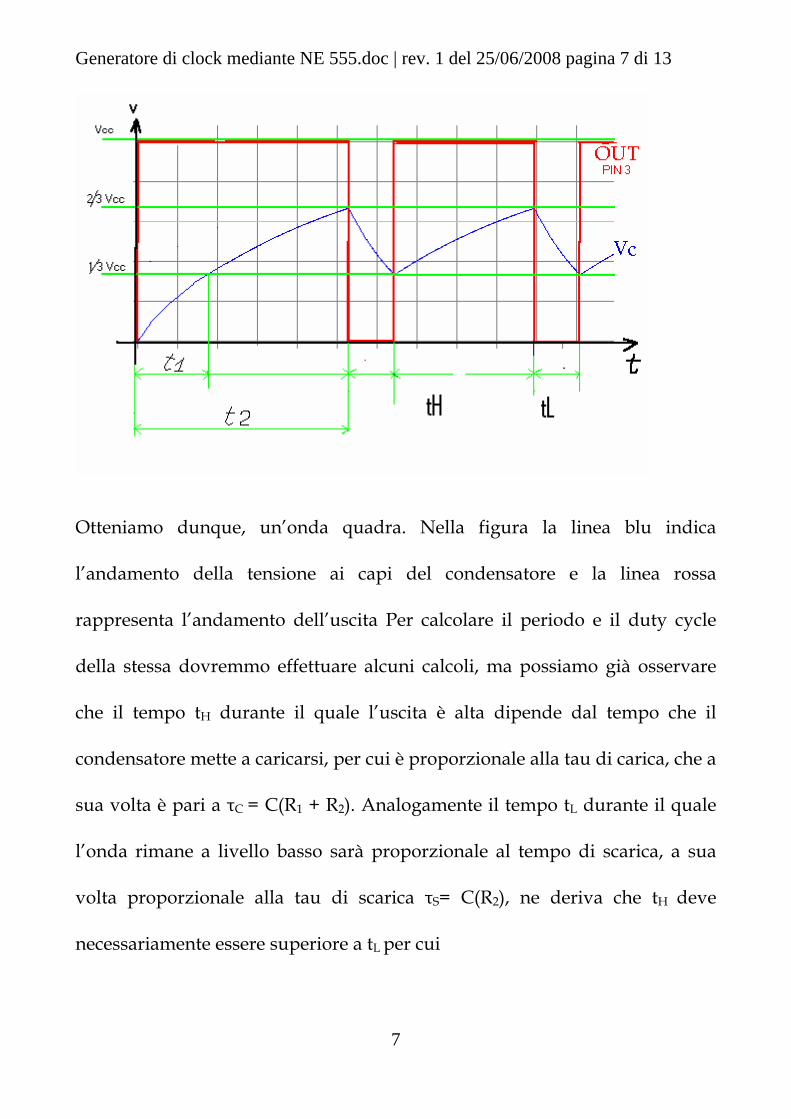
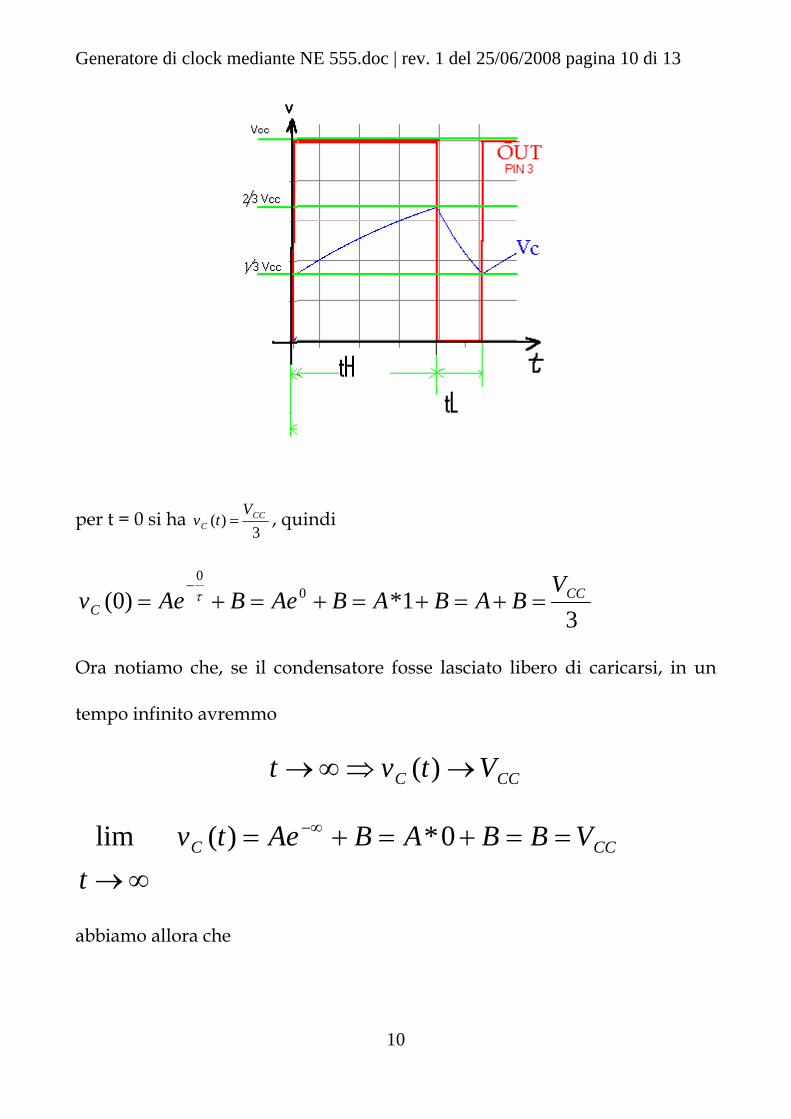
Otteniamo dunque, un’onda quadra. Nella figura la linea blu indica
l’andamento della tensione ai capi del condensatore e la linea rossa
rappresenta l’andamento dell’uscita Per calcolare il periodo e il duty cycle
della stessa dovremmo effettuare alcuni calcoli, ma possiamo già osservare
che il tempo tH durante il quale l’uscita è alta dipende dal tempo che il
condensatore mette a caricarsi, per cui è proporzionale alla tau di carica, che a
sua volta è pari a τC = C(R1 + R2). Analogamente il tempo tL durante il quale
l’onda rimane a livello basso sarà proporzionale al tempo di scarica, a sua
volta proporzionale alla tau di scarica τS= C(R2), ne deriva che tH deve
necessariamente essere superiore a tL per cui
Generatore di clock mediante NE 555.doc | rev. 1 del 25/06/2008 pagina 8 di 13
8
21
>+
=LH
HH
ttt
Tt
cioè il duty cycle è
%50100100% >+
==LH
HH
ttt
TtD
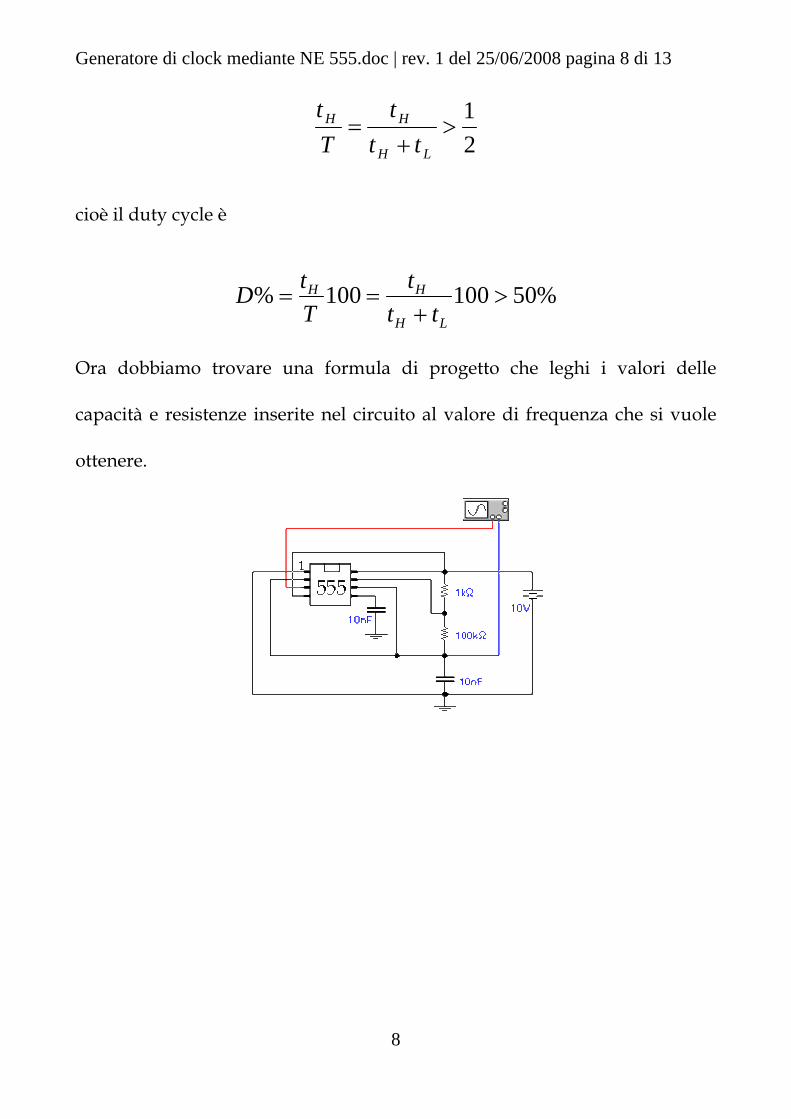
Ora dobbiamo trovare una formula di progetto che leghi i valori delle
capacità e resistenze inserite nel circuito al valore di frequenza che si vuole
ottenere.
Generatore di clock mediante NE 555.doc | rev. 1 del 25/06/2008 pagina 9 di 13
9
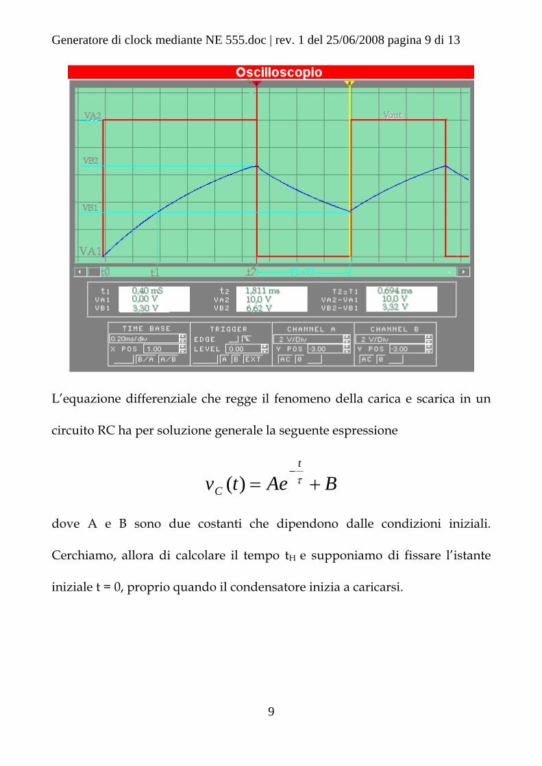
L’equazione differenziale che regge il fenomeno della carica e scarica in un
circuito RC ha per soluzione generale la seguente espressione
BAetvt
C +=−τ)(
dove A e B sono due costanti che dipendono dalle condizioni iniziali.
Cerchiamo, allora di calcolare il tempo tH e supponiamo di fissare l’istante
iniziale t = 0, proprio quando il condensatore inizia a caricarsi.
Generatore di clock mediante NE 555.doc | rev. 1 del 25/06/2008 pagina 10 di 13
10
per t = 0 si ha 3
)( CCC
Vtv = , quindi
31*)0( 0
0CC
CV
BABABAeBAev =+=+=+=+=−τ
Ora notiamo che, se il condensatore fosse lasciato libero di caricarsi, in un
tempo infinito avremmo
CCC Vtvt →⇒∞→ )(
∞→==+=+= −∞
tVBBABAetv CCC 0*)(lim
abbiamo allora che
Generatore di clock mediante NE 555.doc | rev. 1 del 25/06/2008 pagina 11 di 13
11
32
333CC
CCCCCC
CC
CC VV
VB
VA
VB
VBA −=−=−=⇒
⎪⎩
⎪⎨⎧
=
=+
la legge che regola nel nostro caso, la carica e scarica di un condensatore è
allora
CC
tCC
C VeVtv C +−=−τ
32)(
dal grafico si vede che per t = tH , 3
2)( CC
CV
tv = quindi
32
32)( CC
CC
tCC
CVVeVtv C
H
=+−=−τ
⇒=+−−
321
32
C
Ht
e τ ⇒−=−−
132
32
C
Ht
e τ ⇒−=−−
31
32
C
Ht
e τ
⇒=−
21
C
Ht
e τ ⇒=−
21lnln C
Ht
e τ
CRRt
tte
H
CHC
Ht
C
H
)(7.0
2ln2ln21lnln
21 +≈
⇒=⇒−=−⇒=−
ττ
τ

Generatore di clock mediante NE 555.doc | rev. 1 del 25/06/2008 pagina 12 di 13
12
ripetiamo lo stesso procedimento per la scarica, ponendo t = 0 all’istante in
cui comincia a scaricarsi il condensatore
BAetv S
t
C +=−τ)(
per t = 0 si ha 3
*2)( CC
CV
tv = ,
3*21*)0( 0
0CC
CVBABABAeBAev =+=+=+=+=
−τ
Ora notiamo che, se il condensatore fosse lasciato libero di scaricarsi, in un
tempo infinito avremmo
0)( →⇒∞→ tvt C

Generatore di clock mediante NE 555.doc | rev. 1 del 25/06/2008 pagina 13 di 13
13
S
tcc
CCC
C
eVtvVA
t
BBABAetv
τ−
−∞
=⇒=
⇒∞→
==+=+=
32)(
32
00*)(lim
dal grafico si vede che per t = tL , 3
)( CCC
Vtv = quindi
332)( CC
tCC
CVeVtv S
L
==−τ
⇒=−
21
S
Lt
e τ ⇒=−
21lnln S
Lt
e τ
CRt
tt
L
SLS
L
)(7.0
2ln2ln
2≈
⇒=⇒−=− ττ
Il periodo dell’onda quadra è allora
)2(7.07.0)(7.0 12221 RRCRCRRttT LH +=++=+=
CRRf
)2(7.01
21 +=
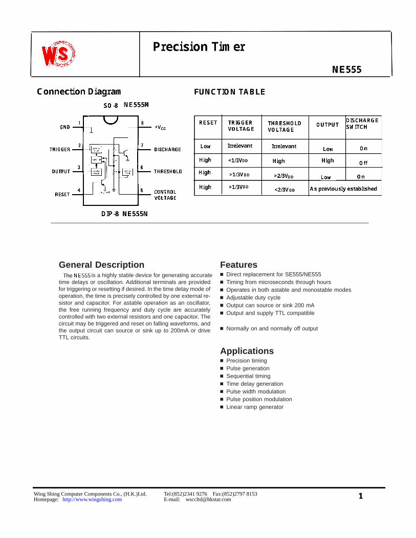
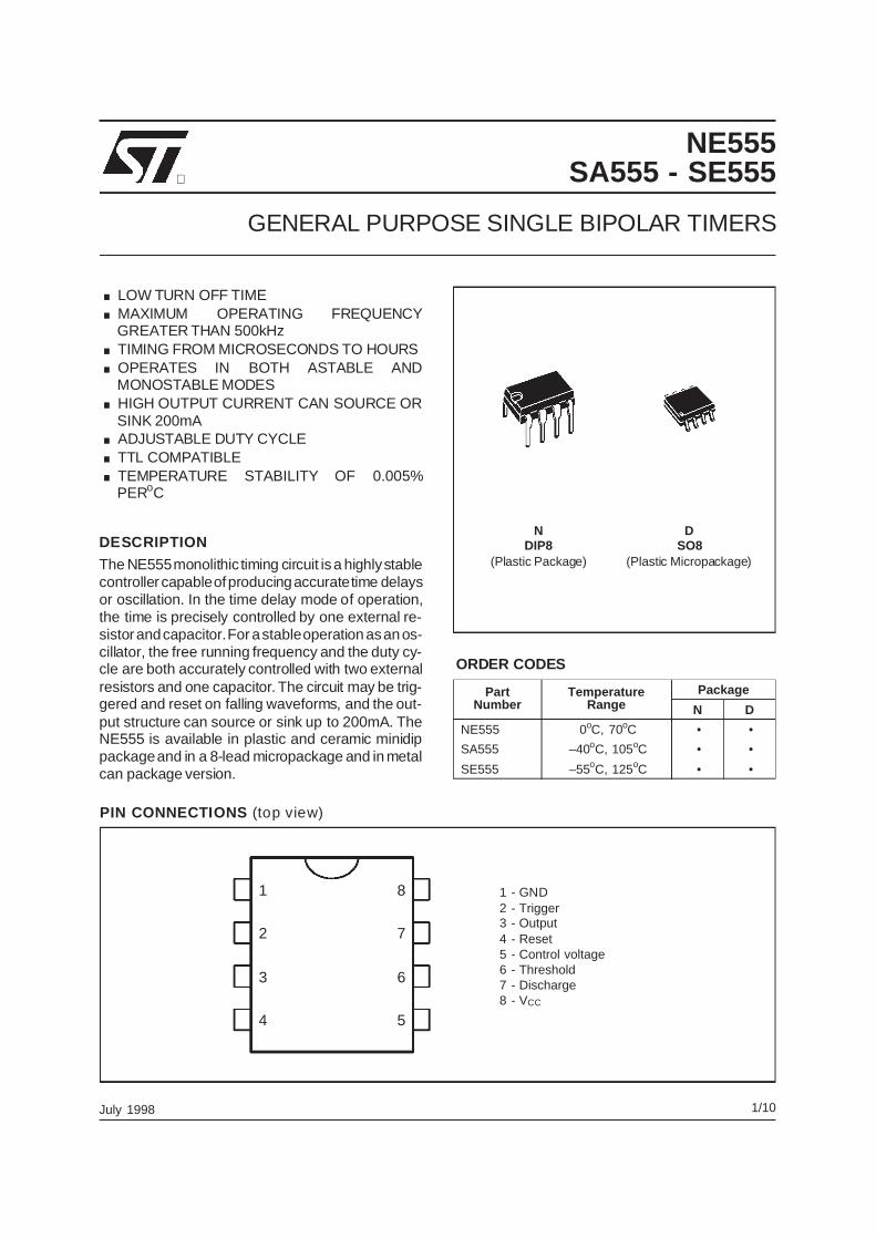
General Descriptionis a highly stable device for generating accurate
time delays or oscillation. Additional terminals are providedfor triggering or resetting if desired. In the time delay mode ofoperation, the time is precisely controlled by one external re-sistor and capacitor. For astable operation as an oscillator,the free running frequency and duty cycle are accuratelycontrolled with two external resistors and one capacitor. Thecircuit may be triggered and reset on falling waveforms, andthe output circuit can source or sink up to 200mA or driveTTL circuits.
Featuresn Direct replacement for SE555/NE555n Timing from microseconds through hoursn Operates in both astable and monostable modesn Adjustable duty cyclen Output can source or sink 200 mAn Output and supply TTL compatible
n Normally on and normally off output
Applicationsn Precision timingn Pulse generationn Sequential timingn Time delay generationn Pulse width modulationn Pulse position modulationn Linear ramp generator
Wing Shing Computer Components Co., (H.K.)Ltd. Tel:(852)2341 9276 Fax:(852)2797 8153Homepage: http://www.wingshing.com E-mail: [email protected]
Tong Lijun
Tong Lijun
Tong Lijun
Tong Lijun
Tong Lijun
Tong Lijun
Tong Lijun
Precision Timer
Tong Lijun
SO-8
Tong Lijun
Tong Lijun
Tong Lijun
Tong Lijun
Tong Lijun
Tong Lijun
Tong Lijun
Tong Lijun
Tong Lijun
Tong Lijun
RESET
Tong Lijun
TRIGGER VOLTAGE
Tong Lijun
THRESHOLD VOLTAGE
Tong Lijun
OUTPUT
Tong Lijun
DISCHARGE SWITCH
Tong Lijun
Low
Tong Lijun
High
Tong Lijun
High
Tong Lijun
High
Tong Lijun
Irrelevant
Tong Lijun
Irrelevant
Tong Lijun
<1/3V
Tong Lijun
>1/3V
Tong Lijun
>1/3V
Tong Lijun
High
Tong Lijun
Low
Tong Lijun
High
Tong Lijun
On
Tong Lijun
Off
Tong Lijun
On
Tong Lijun
Low
Tong Lijun
>2/3V
Tong Lijun
<2/3V
Tong Lijun
DD
Tong Lijun
DD
Tong Lijun
DD
Tong Lijun
DD
Tong Lijun
Tong Lijun
DD
Tong Lijun
As previously established
Tong Lijun
FUNCTION TABLE
Tong Lijun
1
Tong Lijun
Connection Diagram
Tong Lijun
NE555
Tong Lijun
NE555M
Tong Lijun
DIP-8 NE555N
Tong Lijun
The NE555
(TA = 25˚C, VCC = +5V to +15V, unless othewise specified)
Parameter Conditions Limits Units
Min Typ Max
Supply Voltage 4.5 16 V
Supply Current VCC = 5V, RL = ∞VCC = 15V, RL = ∞
310
615 mA
Timing Error, Monostable
Initial Accuracy 1 %
Drift with Temperature RA = 1k to 100kΩ, 50 ppm/˚C
C = 0.1µF, (Note 5)
Accuracy over Temperature 1.5 %
Drift with Supply 0.1 %/V
Timing Error, Astable
Initial Accuracy 2.25 %
Drift with Temperature RA, RB = 1k to 100kΩ, 150 ppm/˚C
C = 0.1µF, (Note 5)
Accuracy over Temperature 3.0 %
Drift with Supply 0.30 %/V
Threshold Voltage 0.667 x VCC
Trigger Voltage VCC = 15V 5 V
VCC = 5V 1.67 V
Trigger Current
Reset Voltage
Reset Current 0.1 0.4 mA
Threshold Current (Note 6)
Control Voltage Level VCC = 15VVCC = 5V
92.6
103.33
114
V
Pin 7 Leakage Output High 1 100 nA
Pin 7 Sat (Note 7)
Output Low VCC = 15V, I7 = 15mA 180 mV
Output Low VCC = 4.5V, I7 = 4.5mA 80 200 mV
LM555
Tong Lijun
Tong Lijun
Tong Lijun
Tong Lijun
Tong Lijun
ELECTRICAL CHARACTERISTICS
Tong Lijun
OUTPUT LOW
Tong Lijun
OUTPUT LOW
Tong Lijun
Vcc=5V,No load OUTPUT HIGH
Tong Lijun
2
Tong Lijun
5
Tong Lijun
Note 4
Tong Lijun
0.5
Tong Lijun
2
Tong Lijun
uA
Tong Lijun
0.3
Tong Lijun
0.7
Tong Lijun
V
Tong Lijun
Tong Lijun
1
Tong Lijun
Reset at Vcc
Tong Lijun
30
Tong Lijun
250
Tong Lijun
nA
Tong Lijun
4.5
Tong Lijun
5.6
Tong Lijun
1.1
Tong Lijun
2.2
Tong Lijun
Trigger at 0V
Tong Lijun
20
Tong Lijun
2
Tong Lijun
Tong Lijun
3
Tong Lijun
0.5
Tong Lijun
NE555
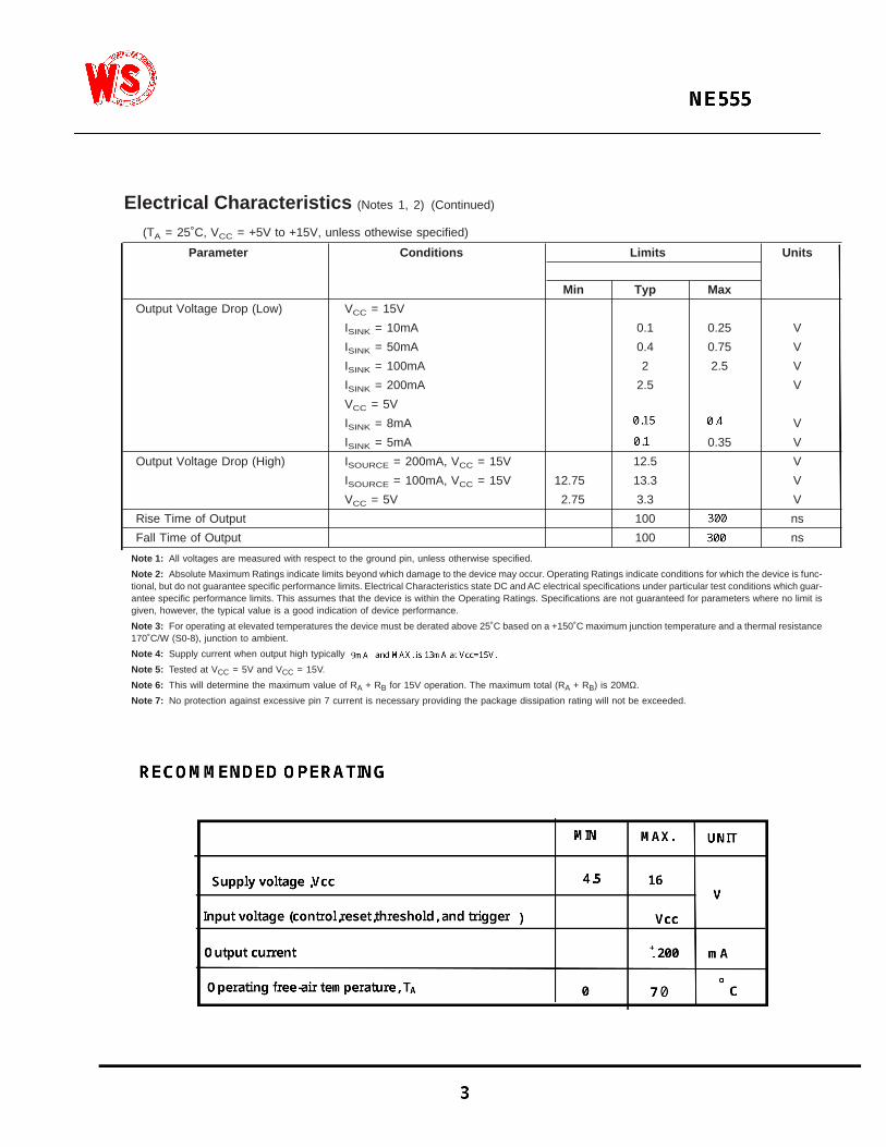
Electrical Characteristics (Notes 1, 2) (Continued)
(TA = 25˚C, VCC = +5V to +15V, unless othewise specified)
Parameter Conditions Limits Units
Min Typ Max
Output Voltage Drop (Low) VCC = 15V
ISINK = 10mA 0.1 0.25 V
ISINK = 50mA 0.4 0.75 V
ISINK = 100mA 2 2.5 V
ISINK = 200mA 2.5 V
VCC = 5V
ISINK = 8mA V
ISINK = 5mA 0.25 0.35 V
Output Voltage Drop (High) ISOURCE = 200mA, VCC = 15V 12.5 V
ISOURCE = 100mA, VCC = 15V 12.75 13.3 V
VCC = 5V 2.75 3.3 V
Rise Time of Output 100 ns
Fall Time of Output 100 ns
Note 1: All voltages are measured with respect to the ground pin, unless otherwise specified.
Note 2: Absolute Maximum Ratings indicate limits beyond which damage to the device may occur. Operating Ratings indicate conditions for which the device is func-tional, but do not guarantee specific performance limits. Electrical Characteristics state DC and AC electrical specifications under particular test conditions which guar-antee specific performance limits. This assumes that the device is within the Operating Ratings. Specifications are not guaranteed for parameters where no limit isgiven, however, the typical value is a good indication of device performance.
Note 3: For operating at elevated temperatures the device must be derated above 25˚C based on a +150˚C maximum junction temperature and a thermal resistance170˚C/W (S0-8), junction to ambient.
Note 4: Supply current when output high typically .
Note 5: Tested at VCC = 5V and VCC = 15V.
Note 6: This will determine the maximum value of RA + RB for 15V operation. The maximum total (RA + RB) is 20MΩ.
Note 7: No protection against excessive pin 7 current is necessary providing the package dissipation rating will not be exceeded.
Tong Lijun
9mA
Tong Lijun
Tong Lijun
and MAX. is 13mA at Vcc=15V.
Tong Lijun
Tong Lijun
Tong Lijun
Tong Lijun
Tong Lijun
0.15
Tong Lijun
0.4
Tong Lijun
0.1
Tong Lijun
Tong Lijun
Tong Lijun
300
Tong Lijun
300
Tong Lijun
Tong Lijun
Tong Lijun
Tong Lijun
Tong Lijun
Tong Lijun
Tong Lijun
Tong Lijun
Tong Lijun
RECOMMENDED OPERATING CONDITIONS
Tong Lijun
Tong Lijun
MIN
Tong Lijun
Tong Lijun
MAX.
Tong Lijun
UNIT
Tong Lijun
Supply voltage ,Vcc
Tong Lijun
Input voltage (control,reset,threshold, and trigger
Tong Lijun
Output current
Tong Lijun
Operating free-air temperature, T
Tong Lijun
A
Tong Lijun
4.5
Tong Lijun
16
Tong Lijun
V
Tong Lijun
Tong Lijun
Vcc
Tong Lijun
+
Tong Lijun
-
Tong Lijun
200
Tong Lijun
mA
Tong Lijun
0
Tong Lijun
70
Tong Lijun
C
Tong Lijun
o
Tong Lijun
Tong Lijun
3
Tong Lijun
)
Tong Lijun
Tong Lijun
NE555
Tong Lijun
0
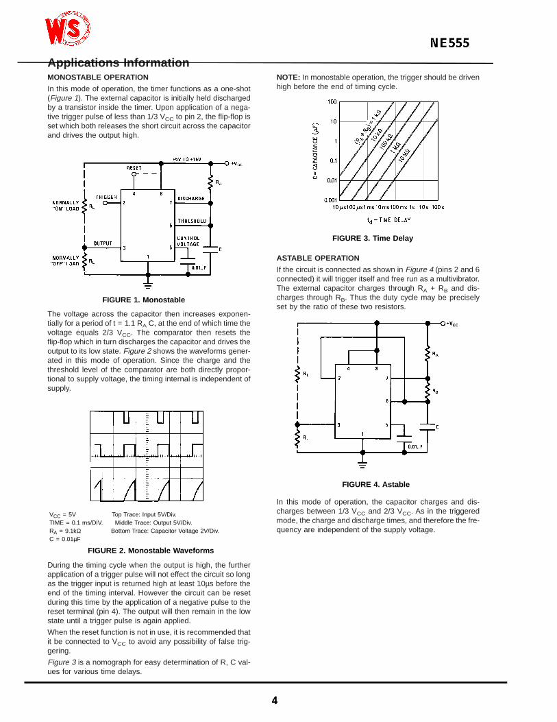
Applications InformationMONOSTABLE OPERATION
In this mode of operation, the timer functions as a one-shot(Figure 1). The external capacitor is initially held dischargedby a transistor inside the timer. Upon application of a nega-tive trigger pulse of less than 1/3 VCC to pin 2, the flip-flop isset which both releases the short circuit across the capacitorand drives the output high.
The voltage across the capacitor then increases exponen-tially for a period of t = 1.1 RA C, at the end of which time thevoltage equals 2/3 VCC. The comparator then resets theflip-flop which in turn discharges the capacitor and drives theoutput to its low state. Figure 2 shows the waveforms gener-ated in this mode of operation. Since the charge and thethreshold level of the comparator are both directly propor-tional to supply voltage, the timing internal is independent ofsupply.
During the timing cycle when the output is high, the furtherapplication of a trigger pulse will not effect the circuit so longas the trigger input is returned high at least 10µs before theend of the timing interval. However the circuit can be resetduring this time by the application of a negative pulse to thereset terminal (pin 4). The output will then remain in the lowstate until a trigger pulse is again applied.
When the reset function is not in use, it is recommended thatit be connected to VCC to avoid any possibility of false trig-gering.
Figure 3 is a nomograph for easy determination of R, C val-ues for various time delays.
NOTE: In monostable operation, the trigger should be drivenhigh before the end of timing cycle.
ASTABLE OPERATION
If the circuit is connected as shown in Figure 4 (pins 2 and 6connected) it will trigger itself and free run as a multivibrator.The external capacitor charges through RA + RB and dis-charges through RB. Thus the duty cycle may be preciselyset by the ratio of these two resistors.
In this mode of operation, the capacitor charges and dis-charges between 1/3 VCC and 2/3 VCC. As in the triggeredmode, the charge and discharge times, and therefore the fre-quency are independent of the supply voltage.
FIGURE 1. Monostable
VCC = 5V Top Trace: Input 5V/Div.TIME = 0.1 ms/DIV. Middle Trace: Output 5V/Div.RA = 9.1kΩ Bottom Trace: Capacitor Voltage 2V/Div.C = 0.01µF
FIGURE 2. Monostable Waveforms
FIGURE 3. Time Delay
FIGURE 4. Astable
Tong Lijun
Tong Lijun
Tong Lijun
4
Tong Lijun
Tong Lijun
Tong Lijun
NE555
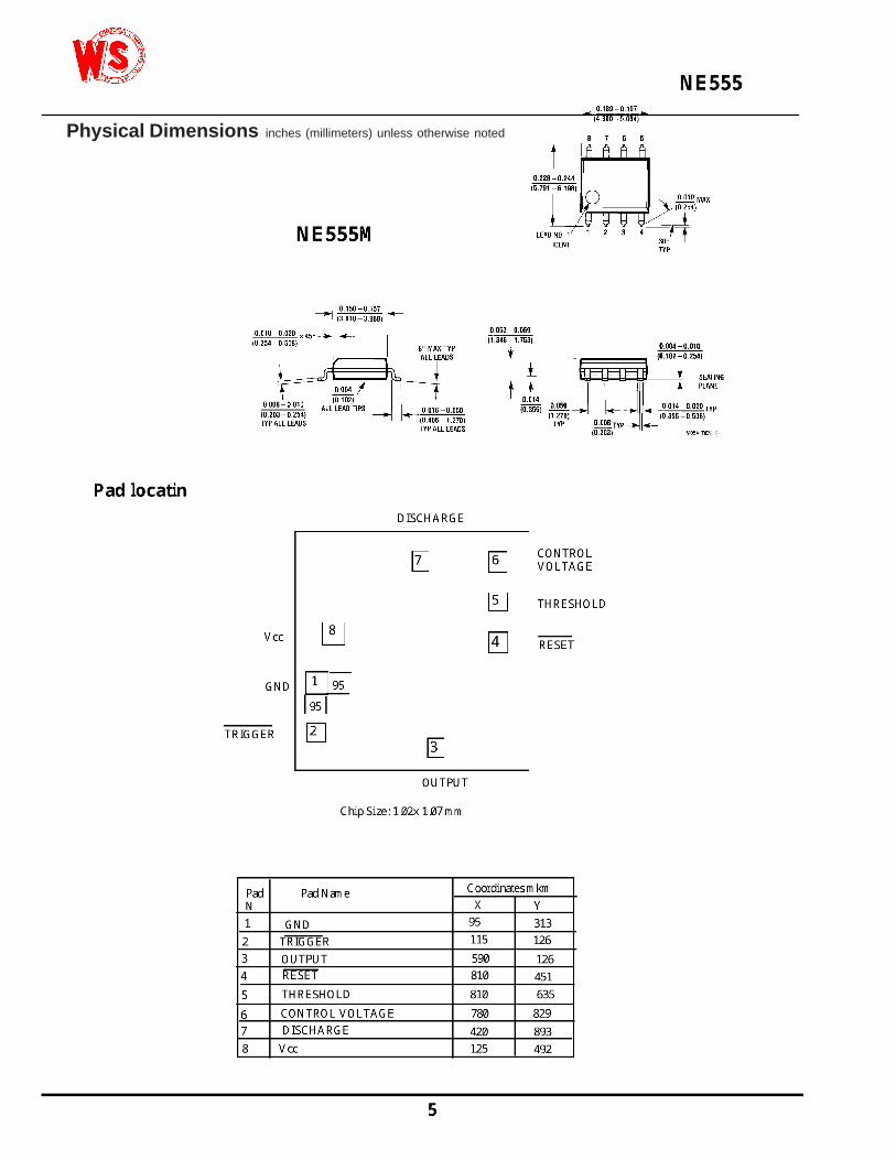
Physical Dimensions inches (millimeters) unless otherwise noted
Tong Lijun
Tong Lijun
Tong Lijun
5
Tong Lijun
Tong Lijun
Tong Lijun
Tong Lijun
Tong Lijun
Tong Lijun
Tong Lijun
Tong Lijun
Tong Lijun
Tong Lijun
Tong Lijun
Tong Lijun
Tong Lijun
Tong Lijun
Tong Lijun
Tong Lijun
1
Tong Lijun
2
Tong Lijun
3
Tong Lijun
4
Tong Lijun
5
Tong Lijun
6
Tong Lijun
7
Tong Lijun
8
Tong Lijun
95
Tong Lijun
Tong Lijun
Tong Lijun
Tong Lijun
Tong Lijun
95
Tong Lijun
OUTPUT
Tong Lijun
RESET
Tong Lijun
Tong Lijun
THRESHOLD
Tong Lijun
CONTROL VOLTAGE
Tong Lijun
DISCHARGE
Tong Lijun
Vcc
Tong Lijun
GND
Tong Lijun
TRIGGER
Tong Lijun
Tong Lijun
Chip Size: 1.02x 1.07 mm
Tong Lijun
Pad locatin
Tong Lijun
Tong Lijun
Tong Lijun
Tong Lijun
Tong Lijun
Tong Lijun
Tong Lijun
Tong Lijun
Tong Lijun
Tong Lijun
Tong Lijun
Tong Lijun
Tong Lijun
Tong Lijun
Tong Lijun
Pad N
Tong Lijun
Pad Name
Tong Lijun
Coordinates mkm
Tong Lijun
Tong Lijun
X
Tong Lijun
Tong Lijun
Y
Tong Lijun
1
Tong Lijun
2
Tong Lijun
3
Tong Lijun
Tong Lijun
Tong Lijun
5
Tong Lijun
4
Tong Lijun
6
Tong Lijun
Tong Lijun
7
Tong Lijun
8
Tong Lijun
GND
Tong Lijun
TRIGGER
Tong Lijun
OUTPUT
Tong Lijun
RESET
Tong Lijun
Tong Lijun
THRESHOLD
Tong Lijun
CONTROL VOLTAGE
Tong Lijun
DISCHARGE
Tong Lijun
Vcc
Tong Lijun
95
Tong Lijun
313
Tong Lijun
115
Tong Lijun
126
Tong Lijun
590
Tong Lijun
126
Tong Lijun
810
Tong Lijun
451
Tong Lijun
810
Tong Lijun
635
Tong Lijun
829
Tong Lijun
780
Tong Lijun
420
Tong Lijun
893
Tong Lijun
125
Tong Lijun
492
Tong Lijun
Tong Lijun
Tong Lijun
Tong Lijun
NE555
Tong Lijun
NE555M

This datasheet has been download from:
www.datasheetcatalog.com
Datasheets for electronics components.
NE/SA/SE555/SE555CTimer
Product dataSupersedes data of 1994 Aug 31
2003 Feb 14
INTEGRATED CIRCUITS

Philips Semiconductors Product data
NE/SA/SE555/SE555CTimer
22003 Feb 14
DESCRIPTIONThe 555 monolithic timing circuit is a highly stable controller capableof producing accurate time delays, or oscillation. In the time delaymode of operation, the time is precisely controlled by one externalresistor and capacitor. For a stable operation as an oscillator, thefree running frequency and the duty cycle are both accuratelycontrolled with two external resistors and one capacitor. The circuitmay be triggered and reset on falling waveforms, and the outputstructure can source or sink up to 200 mA.
FEATURES• Turn-off time less than 2 µs
• Max. operating frequency greater than 500 kHz
• Timing from microseconds to hours
• Operates in both astable and monostable modes
• High output current
• Adjustable duty cycle
• TTL compatible
• Temperature stability of 0.005% per °C
APPLICATIONS• Precision timing
• Pulse generation
• Sequential timing
• Time delay generation
• Pulse width modulation
PIN CONFIGURATION
1
2
3
4 5
6
7
8GND
TRIGGER
OUTPUT
RESET
DISCHARGE
THRESHOLD
CONTROL VOLTAGE
VCC
D and N Packages
SL00349
Figure 1. Pin configuration
BLOCK DIAGRAM
COMPARATOR
COMPARATOR
FLIP FLOP
OUTPUTSTAGE
THRESHOLD
VCC
6
7
3 1
4
2
5
8
R
R
R
CONTROLVOLTAGE
TRIGGER
RESET
DISCHARGE
OUTPUT GND
SL00350
Figure 2. Block Diagram
ORDERING INFORMATIONDESCRIPTION TEMPERATURE RANGE ORDER CODE DWG #
8-Pin Plastic Small Outline (SO) Package 0 to +70 °C NE555D SOT96-1
8-Pin Plastic Dual In-Line Package (DIP) 0 to +70 °C NE555N SOT97-1
8-Pin Plastic Small Outline (SO) Package –40 °C to +85 °C SA555D SOT96-1
8-Pin Plastic Dual In-Line Package (DIP) –40 °C to +85 °C SA555N SOT97-1
8-Pin Plastic Dual In-Line Package (DIP) –55 °C to +125 °C SE555CN SOT97-1
8-Pin Plastic Dual In-Line Package (DIP) –55 °C to +125 °C SE555N SOT97-1
Philips Semiconductors Product data
NE/SA/SE555/SE555CTimer
2003 Feb 14 3
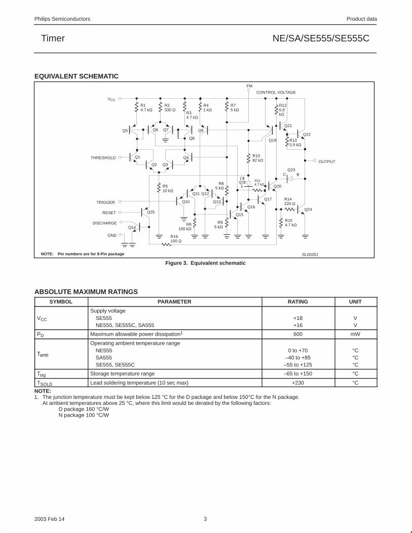
EQUIVALENT SCHEMATIC
NOTE: Pin numbers are for 8-Pin package
CONTROL VOLTAGE
FM
VCC
R14.7 kΩ
R2330 Ω
R34.7 kΩ
R41 kΩ
R75 kΩ
R126.8kΩ
Q21Q9
Q8
Q7Q6Q5
Q1
Q2 Q3
Q4
Q19
Q22
R133.9 kΩ
OUTPUT
Q23C B
R1082 kΩ
R510 kΩ
Q10
Q11 Q12
Q13
Q20R114.7 kΩ
CBQ18
ER8
5 kΩ
Q17
Q16
Q15
R6100 kΩ
R16100 Ω
Q14
Q25
R95 kΩ
R154.7 kΩ
Q24
R14220 Ω
THRESHOLD
TRIGGER
RESET
DISCHARGE
GND
SL00351
Figure 3. Equivalent schematic
ABSOLUTE MAXIMUM RATINGSSYMBOL PARAMETER RATING UNIT
Supply voltageVCC SE555 +18 V
NE555, SE555C, SA555 +16 V
PD Maximum allowable power dissipation1 600 mW
Operating ambient temperature range
TambNE555 0 to +70 °C
Tamb SA555 –40 to +85 °CSE555, SE555C –55 to +125 °C
Tstg Storage temperature range –65 to +150 °C
TSOLD Lead soldering temperature (10 sec max) +230 °CNOTE:1. The junction temperature must be kept below 125 °C for the D package and below 150°C for the N package.
At ambient temperatures above 25 °C, where this limit would be derated by the following factors:D package 160 °C/WN package 100 °C/W

Philips Semiconductors Product data
NE/SA/SE555/SE555CTimer
2003 Feb 14 4
DC AND AC ELECTRICAL CHARACTERISTICSTamb = 25 °C, VCC = +5 V to +15 V unless otherwise specified.
SYMBOL PARAMETER TEST CONDITIONSSE555 NE555/SA555/SE555C
UNITSYMBOL PARAMETER TEST CONDITIONSMin Typ Max Min Typ Max
UNIT
VCC Supply voltage 4.5 18 4.5 16 V
ICC Supply current (low state)1VCC = 5 V, RL = ∞ 3 5 3 6 mA
ICC Su ly current (low state)VCC = 15 V, RL = ∞ 10 12 10 15 mA
Timing error (monostable) RA = 2 kΩ to 100 kΩtM Initial accuracy2 C=0.1 µF 0.5 2.0 1.0 3.0 %∆tM/∆T Drift with temperature 30 100 50 150 ppm/°C∆tM/∆VS Drift with supply voltage 0.05 0.2 0.1 0.5 %/V
Timing error (astable) RA, RB = 1 kΩ to 100 kΩtA Initial accuracy2 C = 0.1 µF 4 6 5 13 %∆tA/∆T Drift with temperature VCC = 15 V 500 500 ppm/°C∆tA/∆VS Drift with supply voltage 0.15 0.6 0.3 1 %/V
VC Control voltage levelVCC = 15 V 9.6 10.0 10.4 9.0 10.0 11.0 V
VC Control voltage levelVCC = 5 V 2.9 3.33 3.8 2.6 3.33 4.0 V
VTH Threshold voltageVCC = 15 V 9.4 10.0 10.6 8.8 10.0 11.2 V
VTH Threshold voltageVCC = 5 V 2.7 3.33 4.0 2.4 3.33 4.2 V
ITH Threshold current3 0.1 0.25 0.1 0.25 µA
VTRIG Trigger voltageVCC = 15 V 4.8 5.0 5.2 4.5 5.0 5.6 V
VTRIG Trigger voltageVCC = 5 V 1.45 1.67 1.9 1.1 1.67 2.2 V
ITRIG Trigger current VTRIG = 0 V 0.5 0.9 0.5 2.0 µA
VRESET Reset voltage4 VCC = 15 V, VTH = 10.5 V 0.3 1.0 0.3 1.0 V
IRESETReset current VRESET = 0.4 V 0.1 0.4 0.1 0.4 mA
IRESET Reset current VRESET = 0 V 0.4 1.0 0.4 1.5 mA
VCC = 15 VISINK = 10 mA 0.1 0.15 0.1 0.25 VISINK = 50 mA 0.4 0.5 0.4 0.75 V
VO LOW level output voltageISINK = 100 mA 2.0 2.2 2.0 2.5 V
VOL LOW-level output voltage ISINK = 200 mA 2.5 2.5 V
VCC = 5 VISINK = 8 mA 0.1 0.25 0.3 0.4 VISINK = 5 mA 0.05 0.2 0.25 0.35 V
VCC = 15 VISOURCE = 200 mA 12.5 12.5 V
VOH HIGH-level output voltage ISOURCE = 100 mA 13.0 13.3 12.75 13.3 VOH g
VCC = 5 VISOURCE = 100 mA 3.0 3.3 2.75 3.3 V
tOFF Turn-off time5 VRESET = VCC 0.5 2.0 0.5 2.0 µs
tR Rise time of output 100 200 100 300 ns
tF Fall time of output 100 200 100 300 ns
Discharge leakage current 20 100 20 100 nA
NOTES:1. Supply current when output high typically 1 mA less.2. Tested at VCC = 5 V and VCC = 15 V.3. This will determine the max value of RA+RB, for 15 V operation, the max total R = 10 MΩ, and for 5 V operation, the max. total R = 3.4 MΩ.4. Specified with trigger input HIGH.5. Time measured from a positive-going input pulse from 0 to 0.8×VCC into the threshold to the drop from HIGH to LOW of the output. Trigger is
tied to threshold.
Philips Semiconductors Product data
NE/SA/SE555/SE555CTimer
2003 Feb 14 5
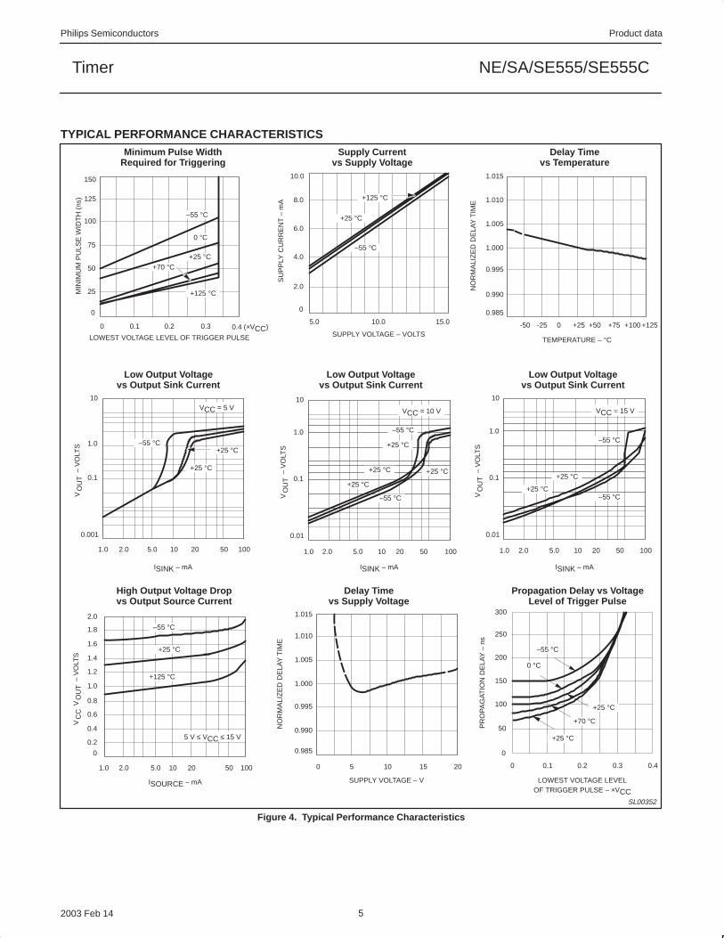
TYPICAL PERFORMANCE CHARACTERISTICSMinimum Pulse Width
Required for TriggeringSupply Current
vs Supply Voltage
Low Output Voltagevs Output Sink Current
Low Output Voltagevs Output Sink Current
Low Output Voltagevs Output Sink Current
Delay Timevs Temperature
Delay Timevs Supply Voltage
Propagation Delay vs VoltageLevel of Trigger Pulse
High Output Voltage Dropvs Output Source Current
MIN
IMU
M P
ULS
E W
IDT
H (
ns)
LOWEST VOLTAGE LEVEL OF TRIGGER PULSE
150
125
100
75
50
25
0
0 0.1 0.2 0.3 0.4 (×VCC)
–55 °C
0 °C
+25 °C+70 °C
+125 °C
10.0
8.0
6.0
4.0
2.0
0
5.0 10.0 15.0
SUPPLY VOLTAGE – VOLTS
SU
PP
LY C
UR
RE
NT
– m
A
1.015
1.010
1.005
1.000
0.995
0.990
0.985
-50 -25 0 +25 +50 +75 +100 +125
NO
RM
ALI
ZE
D D
ELA
Y T
IME
TEMPERATURE – °C
10
1.0
0.1
0.001
1.0 2.0 5.0 10 20 50 100
10
1.0
0.1
0.01
1.0 2.0 5.0 10 20 50 100
10
1.0
0.1
0.01
1.0 2.0 5.0 10 20 50 100
1.0 2.0 5.0 10 20 50 100
2.0
1.8
1.6
1.4
1.2
1.0
0.8
0.6
0.4
0.2
0
1.015
1.010
1.005
1.000
0.995
0.990
0.985
0 5 10 15 20 0 0.1 0.2 0.3 0.4
300
250
200
150
100
50
0
V
– V
OLT
SO
UT
V
– V
OLT
SO
UT
V
– V
OLT
SO
UT
V
– V
OLT
SO
UT
V C
C
NO
RM
ALI
ZE
D D
ELA
Y T
IME
PR
OP
AG
AT
ION
DE
LAY
– n
s
ISINK – mA ISINK – mA ISINK – mA
ISOURCE – mA SUPPLY VOLTAGE – V LOWEST VOLTAGE LEVELOF TRIGGER PULSE – ×VCC
+125 °C
+25 °C
–55 °C
VCC = 5 V VCC = 10 V VCC = 15 V
–55 °C
+25 °C
+25 °C
–55 °C
+25 °C
+25 °C+25 °C
+25 °C
–55 °C
–55 °C
–55 °C
+25 °C
+25 °C
–55 °C
+25 °C
+125 °C
5 V ≤ VCC ≤ 15 V
–55 °C
0 °C
+25 °C
+70 °C
+25 °C
SL00352
Figure 4. Typical Performance Characteristics

Philips Semiconductors Product data
NE/SA/SE555/SE555CTimer
2003 Feb 14 6
TYPICAL APPLICATIONS
OUTPUTFLIPFLOP
COMP
COMP
f 1.49(RA 2RB)C
555 OR 1/2 556
DISCHARGE
CONTROLVOLTAGE
THRESHOLD
TRIGGER
RESET
OUTPUT
R
R
C
RB
RA
R
5
6
2
4
3
8
7
0.01 µF
VCC
OUTPUTFLIPFLOP
COMP
COMP
555 OR 1/2 556
DISCHARGE
CONTROLVOLTAGE
THRESHOLD
TRIGGER
RESET
OUTPUT
R
R
RA
R
5
6
2
4
3
8
7
0.01 µF
VCC
∆T = 1.1RC
C
13
VCC
| ∆t |
Astable Operation
Monostable Operation SL00353
Figure 5. Typical Applications
Philips Semiconductors Product data
NE/SA/SE555/SE555CTimer
2003 Feb 14 7
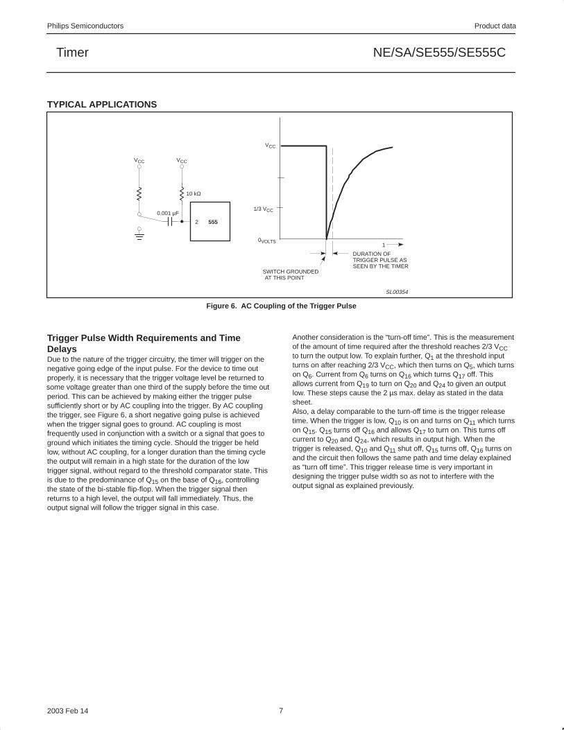
TYPICAL APPLICATIONS
DURATION OF TRIGGER PULSE AS SEEN BY THE TIMER
VCC VCC
10 kΩ
2 555
0.001 µF
1
SWITCH GROUNDEDAT THIS POINT
0VOLTS
1/3 VCC
VCC
SL00354
Figure 6. AC Coupling of the Trigger Pulse
Trigger Pulse Width Requirements and TimeDelaysDue to the nature of the trigger circuitry, the timer will trigger on thenegative going edge of the input pulse. For the device to time outproperly, it is necessary that the trigger voltage level be returned tosome voltage greater than one third of the supply before the time outperiod. This can be achieved by making either the trigger pulsesufficiently short or by AC coupling into the trigger. By AC couplingthe trigger, see Figure 6, a short negative going pulse is achievedwhen the trigger signal goes to ground. AC coupling is mostfrequently used in conjunction with a switch or a signal that goes toground which initiates the timing cycle. Should the trigger be heldlow, without AC coupling, for a longer duration than the timing cyclethe output will remain in a high state for the duration of the lowtrigger signal, without regard to the threshold comparator state. Thisis due to the predominance of Q15 on the base of Q16, controllingthe state of the bi-stable flip-flop. When the trigger signal thenreturns to a high level, the output will fall immediately. Thus, theoutput signal will follow the trigger signal in this case.
Another consideration is the “turn-off time”. This is the measurementof the amount of time required after the threshold reaches 2/3 VCCto turn the output low. To explain further, Q1 at the threshold inputturns on after reaching 2/3 VCC, which then turns on Q5, which turnson Q6. Current from Q6 turns on Q16 which turns Q17 off. Thisallows current from Q19 to turn on Q20 and Q24 to given an outputlow. These steps cause the 2 µs max. delay as stated in the datasheet.Also, a delay comparable to the turn-off time is the trigger releasetime. When the trigger is low, Q10 is on and turns on Q11 which turnson Q15. Q15 turns off Q16 and allows Q17 to turn on. This turns offcurrent to Q20 and Q24, which results in output high. When thetrigger is released, Q10 and Q11 shut off, Q15 turns off, Q16 turns onand the circuit then follows the same path and time delay explainedas “turn off time”. This trigger release time is very important indesigning the trigger pulse width so as not to interfere with theoutput signal as explained previously.

Philips Semiconductors Product data
NE/SA/SE555/SE555CTimer
2003 Feb 14 8
SO8: plastic small outline package; 8 leads; body width 3.9 mm SOT96-1

Philips Semiconductors Product data
NE/SA/SE555/SE555CTimer
2003 Feb 14 9
DIP8: plastic dual in-line package; 8 leads (300 mil) SOT97-1

Philips Semiconductors Product data
NE/SA/SE555/SE555CTimer
2003 Feb 14 10
REVISION HISTORY
Rev Date Description
_2 20030214 Product data (9397 750 11129); ECN 853-0036 29156 of 06 November 2002. Supersedes Product specification dated August 31, 1994.
Modifications:
• Remove all cerdip information from the data sheet. Package type discontinued.
• ‘Absolute maximum ratings’ table: TSOLD rating changed from ‘+300 °C’ to ‘+230 °C’.
19940831 Product specification; ECN 853-0036 13721 of 31 August 1994.
(Filename = NE_SA555X.pdf)
Philips Semiconductors Product data
NE/SA/SE555/SE555CTimer
2003 Feb 14 11
DefinitionsShort-form specification — The data in a short-form specification is extracted from a full data sheet with the same type number and title. For detailed information seethe relevant data sheet or data handbook.
Limiting values definition — Limiting values given are in accordance with the Absolute Maximum Rating System (IEC 60134). Stress above one or more of the limitingvalues may cause permanent damage to the device. These are stress ratings only and operation of the device at these or at any other conditions above those givenin the Characteristics sections of the specification is not implied. Exposure to limiting values for extended periods may affect device reliability.
Application information — Applications that are described herein for any of these products are for illustrative purposes only. Philips Semiconductors make norepresentation or warranty that such applications will be suitable for the specified use without further testing or modification.
DisclaimersLife support — These products are not designed for use in life support appliances, devices, or systems where malfunction of these products can reasonably beexpected to result in personal injury. Philips Semiconductors customers using or selling these products for use in such applications do so at their own risk and agreeto fully indemnify Philips Semiconductors for any damages resulting from such application.
Right to make changes — Philips Semiconductors reserves the right to make changes in the products—including circuits, standard cells, and/or software—describedor contained herein in order to improve design and/or performance. When the product is in full production (status ‘Production’), relevant changes will be communicatedvia a Customer Product/Process Change Notification (CPCN). Philips Semiconductors assumes no responsibility or liability for the use of any of these products, conveysno license or title under any patent, copyright, or mask work right to these products, and makes no representations or warranties that these products are free from patent,copyright, or mask work right infringement, unless otherwise specified.
Contact informationFor additional information please visithttp://www.semiconductors.philips.com . Fax: +31 40 27 24825
For sales offices addresses send e-mail to:[email protected] .
Koninklijke Philips Electronics N.V. 2003All rights reserved. Printed in U.S.A.
Date of release: 02-03
Document order number: 9397 750 11129
Data sheet status [1]
Objective data
Preliminary data
Product data
Productstatus [2] [3]
Development
Qualification
Production
Definitions
This data sheet contains data from the objective specification for product development.Philips Semiconductors reserves the right to change the specification in any manner without notice.
This data sheet contains data from the preliminary specification. Supplementary data will be publishedat a later date. Philips Semiconductors reserves the right to change the specification without notice, inorder to improve the design and supply the best possible product.
This data sheet contains data from the product specification. Philips Semiconductors reserves theright to make changes at any time in order to improve the design, manufacturing and supply. Relevantchanges will be communicated via a Customer Product/Process Change Notification (CPCN).
Data sheet status
[1] Please consult the most recently issued data sheet before initiating or completing a design.
[2] The product status of the device(s) described in this data sheet may have changed since this data sheet was published. The latest information is available on the Internet at URLhttp://www.semiconductors.philips.com.
[3] For data sheets describing multiple type numbers, the highest-level product status determines the data sheet status.
Level
I
II
III

This datasheet has been download from:
www.datasheetcatalog.com
Datasheets for electronics components.
July 1998
®
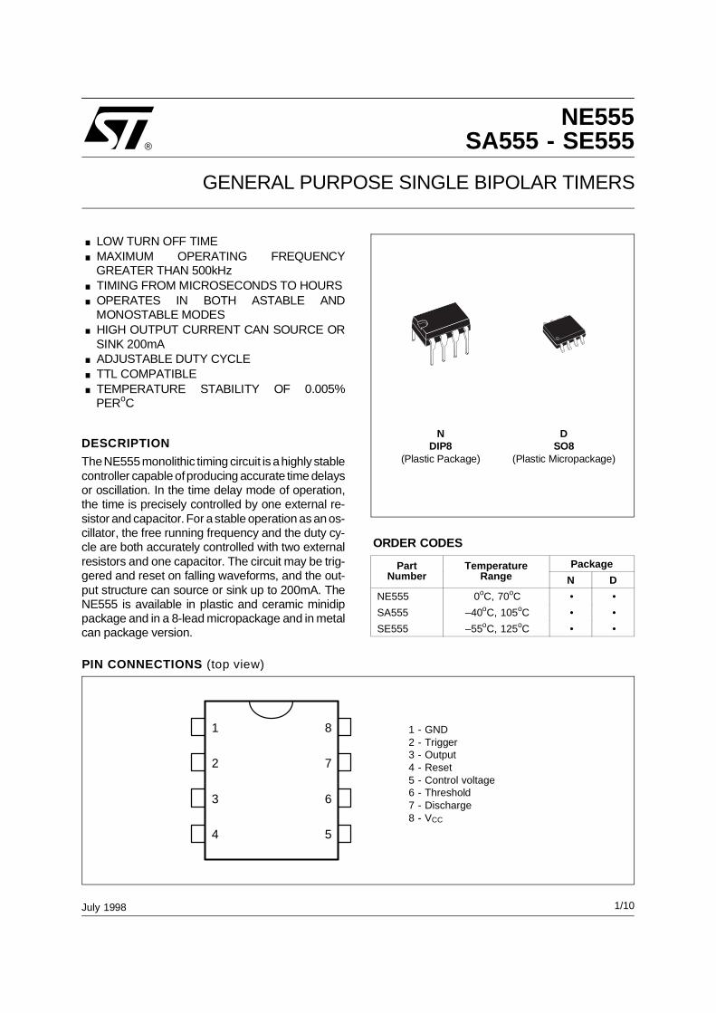
NDIP8
(Plastic Package)
DSO8
(Plastic Micropackage)
1
2
3
4 5
6
7
8 1 - GND2 - Trigger3 - Output4 - Reset5 - Control voltage6 - Threshold7 - Discharge8 - VCC
PIN CONNECTIONS (top view)
. LOW TURN OFF TIME.MAXIMUM OPERATING FREQUENCYGREATER THAN 500kHz.TIMING FROM MICROSECONDS TO HOURS.OPERATES IN BOTH ASTABLE ANDMONOSTABLE MODES.HIGH OUTPUT CURRENT CAN SOURCE ORSINK 200mA.ADJUSTABLE DUTY CYCLE.TTL COMPATIBLE.TEMPERATURE STABILITY OF 0.005%PERoC
ORDER CODES
PartNumber
TemperatureRange
Package
N D
NE555 0oC, 70oC • •SA555 –40oC, 105oC • •SE555 –55oC, 125oC • •
DESCRIPTION
The NE555 monolithic timing circuit is a highly stablecontroller capable of producing accurate time delaysor oscillation. In the time delay mode of operation,the time is precisely controlled by one external re-sistor and capacitor. For a stable operation as an os-cillator, the free running frequency and the duty cy-cle are both accurately controlled with two externalresistors and one capacitor. The circuit may be trig-gered and reset on falling waveforms, and the out-put structure can source or sink up to 200mA. TheNE555 is available in plastic and ceramic minidippackage and in a 8-lead micropackage and in metalcan package version.
NE555SA555 - SE555
GENERAL PURPOSE SINGLE BIPOLAR TIMERS
1/10
THRESHOLD
COMP
5kΩ
5kΩ
5kΩ
TRIGGER
R
FLIP-FLOP
S
Q
DISCHARGE
OUT
INHIBIT/
RESET
RESET
COMP
S - 8086
S
+
CONTROL VOLTAGE
VCC
BLOCK DIAGRAM
OUTPUT
CONTROLVOLTAGE
THRESHOLDCOMPARATOR
VCC
R14.7kW
R2830W
Q5 Q6 Q7 Q8 Q9
R34.7kW
R41kW
R85kW
Q1
Q2 Q3
Q4
Q10
Q11 Q12
Q13
THRESHOLD
TRIGGER
RESET
DISCHARGE
G N D
2
4
7
1
Q14
Q15
R510kW
R6100kW
R7100kW
R105kW
Q17
Q16 Q18
R95kW D2
R16100W
R154.7kW
R14220W
Q24
Q23
R174.7kW
3
Q22
R13
D1
Q19Q20
Q21
R126.8kW
5
TRIGGER COMPARATOR FLIP FLOP
R115kW
3.9kW
SCHEMATIC DIAGRAM
ABSOLUTE MAXIMUM RATINGS
Symbol Parameter Value Unit
Vcc Supply Voltage 18 V
Toper Operating Free Air Temperature Range for NE555for SA555for SE555
0 to 70–40 to 105–55 to 125
oC
Tj Junction Temperature 150 oC
Tstg Storage Temperature Range –65 to 150 oC
NE555/SA555/SE555
2/10

ELECTRICAL CHARACTERISTICSTamb = +25oC, VCC = +5V to +15V (unless otherwise specified)
Symbol ParameterSE555 NE555 - SA555
UnitMin. Typ. Max. Min. Typ. Max.
ICC Supply Current (RL ∞) (- note 1)Low State VCC = +5V
VCC = +15VHigh State VCC = 5V
3102
512
3102
615
mA
Timing Error (monostable)(RA = 2k to 100kΩ, C = 0.1µF)Initial Accuracy - (note 2)Drift with TemperatureDrift with Supply Voltage
0.530
0.05
21000.2
1500.1
3
0.5
%ppm/°C
%/V
Timing Error (astable)(RA, RB = 1kΩ to 100kΩ, C = 0.1µF,VCC = +15V) Initial Accuracy - (note 2)Drift with TemperatureDrift with Supply Voltage
1.590
0.15
2.251500.3
%ppm/°C
%/V
VCL Control Voltage levelVCC = +15VVCC = +5V
9.62.9
103.33
10.43.8
92.6
103.33
114
V
Vth Threshold VoltageVCC = +15VVCC = +5V
9.42.7
103.33
10.64
8.82.4
103.33
11.24.2
V
Ith Threshold Current - (note 3) 0.1 0.25 0.1 0.25 µA
Vtrig Trigger VoltageVCC = +15VVCC = +5V
4.81.45
51.67
5.21.9
4.51.1
51.67
5.62.2
V
Itrig Trigger Current (Vtrig = 0V) 0.5 0.9 0.5 2.0 µA
Vreset Reset Voltage - (note 4) 0.4 0.7 1 0.4 0.7 1 V
Ireset Reset CurrentVreset = +0.4VVreset = 0V
0.10.4
0.41
0.10.4
0.41.5
mA
VOL Low Level Output VoltageVCC = +15V, IO(sink) = 10mA
IO(sink) = 50mAIO(sink) = 100mAIO(sink) = 200mA
VCC = +5V, IO(sink) = 8mAIO(sink) = 5mA
0.10.42
2.50.1
0.05
0.150.52.2
0.250.2
0.10.42
2.50.3
0.25
0.250.752.5
0.40.35
V
VOH High Level Output VoltageVCC = +15V, IO(source) = 200mA
IO(source) = 100mAVCC = +5V, IO(source) = 100mA
133
12.513.33.3
12.752.75
12.513.33.3
V
Notes : 1. Supply current when output is high is typically 1mA less.2. Tested at VCC = +5V and VCC = +15V.3. This will determine the maximum value of RA + RB for +15V operation the max total is R = 20MΩ and for 5V operation
the max total R = 3.5MΩ.
OPERATING CONDITIONS
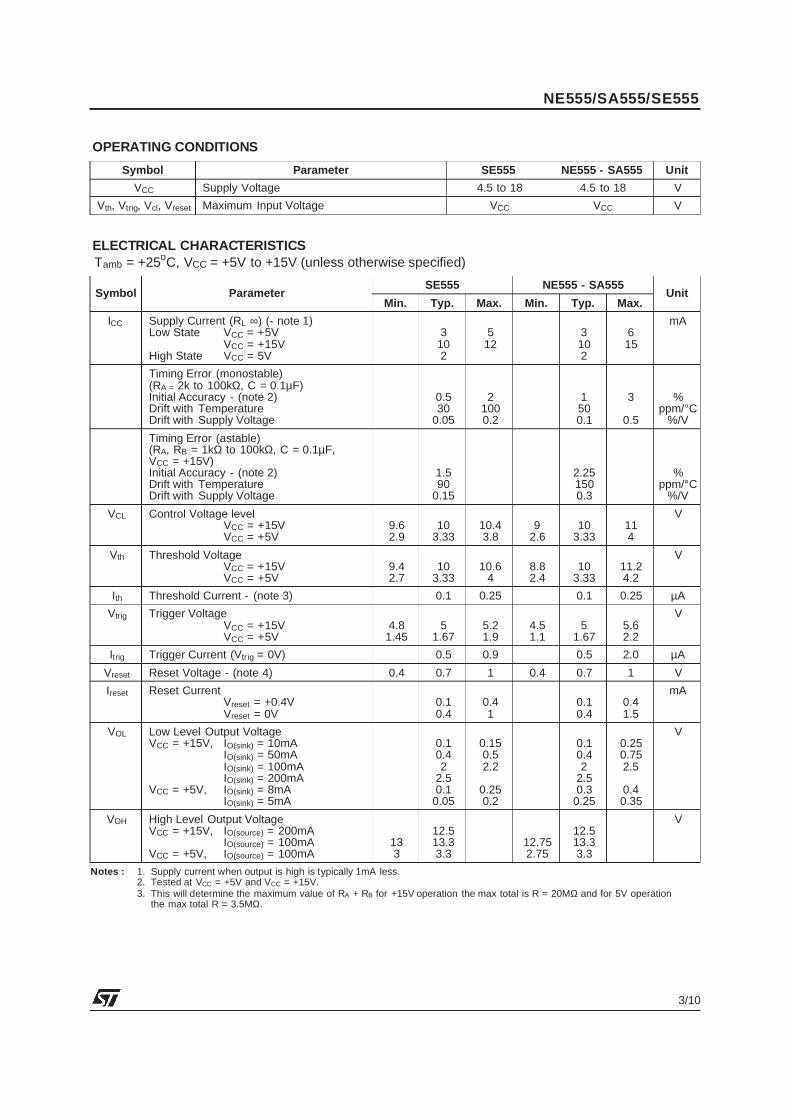
Symbol Parameter SE555 NE555 - SA555 Unit
VCC Supply Voltage 4.5 to 18 4.5 to 18 V
Vth, Vtrig, Vcl, Vreset Maximum Input Voltage VCC VCC V
NE555/SA555/SE555
3/10
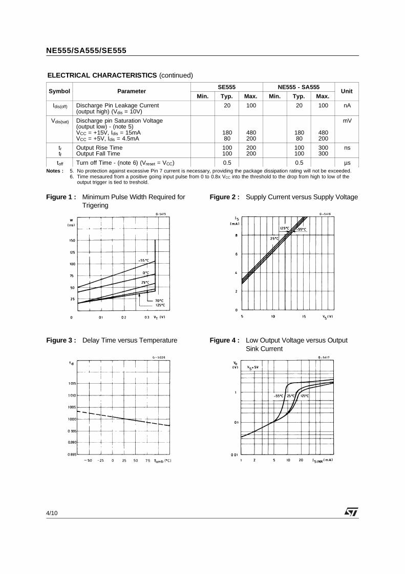
ELECTRICAL CHARACTERISTICS (continued)
Symbol ParameterSE555 NE555 - SA555
UnitMin. Typ. Max. Min. Typ. Max.
Idis(off) Discharge Pin Leakage Current(output high) (Vdis = 10V)
20 100 20 100 nA
Vdis(sat) Discharge pin Saturation Voltage(output low) - (note 5)VCC = +15V, Idis = 15mAVCC = +5V, Idis = 4.5mA
18080
480200
18080
480200
mV
trtf
Output Rise TimeOutput Fall Time
100100
200200
100100
300300
ns
toff Turn off Time - (note 6) (Vreset = VCC) 0.5 0.5 µsNotes : 5. No protection against excessive Pin 7 current is necessary, providing the package dissipation rating will not be exceeded.
6. Time mesaured from a positive going input pulse from 0 to 0.8x VCC into the threshold to the drop from high to low of theoutput trigger is tied to treshold.
Figure 1 : Minimum Pulse Width Required forTrigering
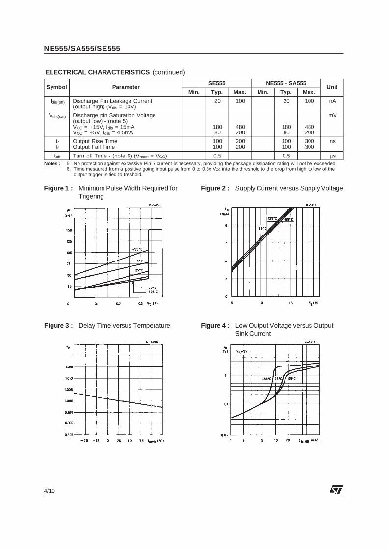
Figure 2 : Supply Current versus Supply Voltage
Figure 3 : Delay Time versus Temperature Figure 4 : Low Output Voltage versus OutputSink Current
NE555/SA555/SE555
4/10
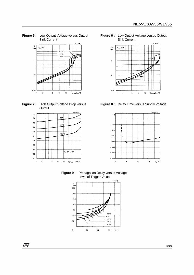
Figure 5 : Low Output Voltage versus OutputSink Current
Figure 6 : Low Output Voltage versus OutputSink Current
Figure 7 : High Output Voltage Drop versusOutput
Figure 8 : Delay Time versus Supply Voltage
Figure 9 : Propagation Delay versus VoltageLevel of Trigger Value
NE555/SA555/SE555
5/10

CAPACITOR VOLTAGE = 2.0V/div
t = 0.1 ms / div
INPUT = 2.0V/div
OUTPUT VOLTAGE = 5.0V/div
R1 = 9.1kΩ, C1 = 0.01µF, R = 1kΩL
Figure 11
Reset
Trigger
Output
R1
C1
Control Voltage
0.01µF
NE555
= 5 to 15VVCC
4
2
3
1
5
6
7
8
Figure 10
C(µF)10
1.0
0.1
0.01
0.00110 100 1.0 10 100 10 (t )dµs µs ms ms ms s
10M
Ω1MΩ10
0kΩ10
kΩR1= 1
kΩ
Figure 12
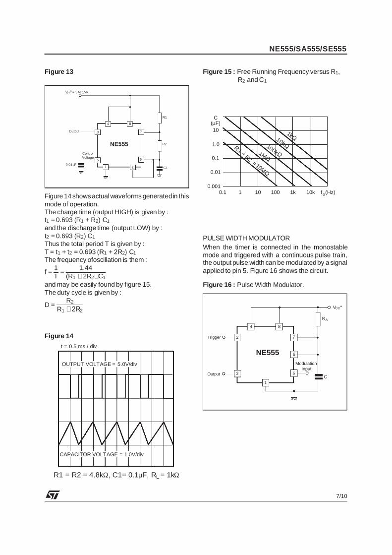
APPLICATION INFORMATION
MONOSTABLE OPERATIONIn the monostable mode, the timer functions as aone-shot. Referring to figure 10 the external capaci-tor is initially held discharged by a transistor insidethe timer.
The circuit triggers on a negative-going input signalwhen the level reaches 1/3 Vcc. Once triggered, thecircuit remains in this state until the set time haselapsed, even if it is triggered again during this in-terval. The duration of the output HIGH state is givenby t = 1.1 R1C1 and is easily determined by figure 12.Notice that since the charge rate and the thresholdlevel of the comparator are both directly proportionalto supply voltage, the timing interval is independentof supply. Applying a negative pulse simultaneouslyto the reset terminal (pin 4) and the trigger terminal(pin 2) during the timing cycle discharges the exter-nal capacitor and causes the cycle to start over. Thetiming cycle now starts on the positive edge of thereset pulse. During the time the reset pulse in ap-plied, the output is driven to its LOW state.When a negative trigger pulse is applied to pin 2, theflip-flop is set, releasing the short circuit across theexternal capacitor and driving the output HIGH. Thevoltage across the capacitor increases exponen-tially with the time constant τ = R1C1. When the volt-age across the capacitor equals 2/3 Vcc, the compa-rator resets the flip-flop which then discharge the ca-pacitor rapidly and drivers the output to its LOWstate.Figure 11 shows the actual waveforms generated inthis mode of operation.When Reset is not used, it should be tied high toavoid any possibly or false triggering.
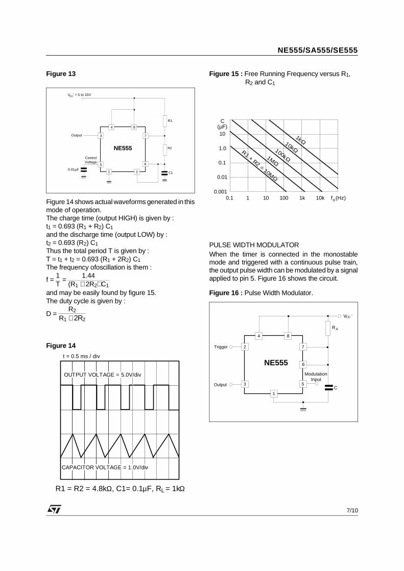
ASTABLE OPERATIONWhen the circuit is connected as shown in figure 13(pin 2 and 6 connected) it triggers itself and free runsas a multivibrator. The external capacitor chargesthrough R1 and R2 and discharges through R2 only.Thus the duty cycle may be precisely set by the ratioof these two resistors.In the astable mode of operation, C1 charges anddischarges between 1/3 Vcc and 2/3 Vcc. As in thetriggered mode, the charge and discharge times andtherefore frequency are independent of the supplyvoltage.
NE555/SA555/SE555
6/10
t = 0.5 ms / div
OUTPUT VOLTAGE = 5.0V/div
CAPACITOR VOLTAGE = 1.0V/div
R1 = R2 = 4.8kΩ, C1= 0.1µF, R = 1kΩL
Figure 14
C(µF)10
1.0
0.1
0.01
0.0010.1 1 10 100 1k 10k f (Hz)o
1MΩ
R1 + R2 = 10MΩ
100kΩ
10kΩ
1kΩ
Figure 15 : Free Running Frequency versus R1,R2 and C1
Figure 14 shows actual waveforms generated in thismode of operation.The charge time (output HIGH) is given by :t1 = 0.693 (R1 + R2) C1
and the discharge time (output LOW) by :t2 = 0.693 (R2) C1
Thus the total period T is given by :T = t1 + t2 = 0.693 (R1 + 2R2) C1
The frequency ofoscillation is them :
f = 1T
= 1.44
(R1 + 2R2) C1
and may be easily found by figure 15.The duty cycle is given by :
D = R2
R1 + 2R2
Output 3
4 8
7
5
1
R1
C12
6
R2
ControlVoltage
NE555
VCC = 5 to 15V
0.01µF
Figure 13
PULSE WIDTH MODULATORWhen the timer is connected in the monostablemode and triggered with a continuous pulse train,the output pulse width can be modulated by a signalapplied to pin 5. Figure 16 shows the circuit.
Trigger
Output
R
C
NE555
2
4
3
1
5
6
7
ModulationInput
8
A
VCC
Figure 16 : Pulse Width Modulator.
NE555/SA555/SE555
7/10
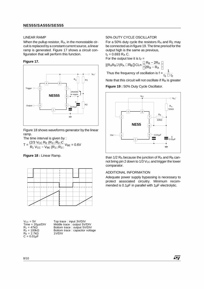
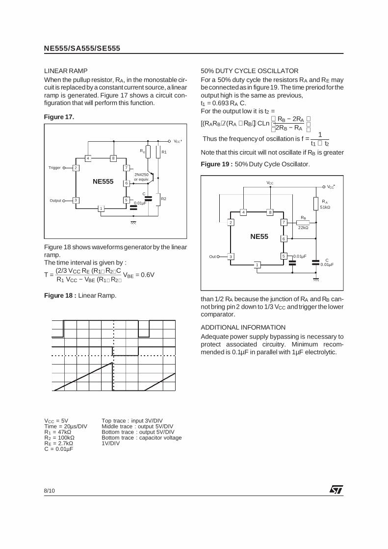
LINEAR RAMPWhen the pullup resistor, RA, in the monostable cir-cuit is replaced by a constant current source, a linearramp is generated. Figure 17 shows a circuit con-figuration that will perform this function.
Trigger
Output
C
NE555
2
4
3
1
5
6
7
8
E
VCC
0.01µFR2
R1R
2N4250or equiv.
Figure 17.
Out
RA
C
NE55
2
4
3
1
5
6
7
8
VCC
51kΩ
RB
22kΩ
0.01µF
VCC
0.01µF
Figure 19 : 50% Duty Cycle Oscillator.
Figure 18 shows waveforms generator by the linearramp.The time interval is given by :
T = (2/3 VCC RE (R1+ R2) CR1 VCC − VBE (R1+ R2)
VBE = 0.6V
Figure 18 : Linear Ramp.
VCC = 5V Top trace : input 3V/DIVTime = 20µs/DIV Middle trace : output 5V/DIVR1 = 47kΩ Bottom trace : output 5V/DIVR2 = 100kΩ Bottom trace : capacitor voltageRE = 2.7kΩ 1V/DIVC = 0.01µF
50% DUTY CYCLE OSCILLATORFor a 50% duty cycle the resistors RA and RE maybe connected as in figure 19. The time preriod for theoutput high is the same as previous,t1 = 0.693 RA C.For the output low it is t2 =
[(RARB) ⁄ (RA + RB)] CLn RB − 2RA
2RB − RA
Thus the frequency of oscillation is f = 1t1 + t2
Note that this circuit will not oscillate if RB is greater
than 1/2 RA because the junction of RA and RB can-not bring pin 2 down to 1/3 VCC and trigger the lowercomparator.
ADDITIONAL INFORMATIONAdequate power supply bypassing is necessary toprotect associated circuitry. Minimum recom-mended is 0.1µF in parallel with 1µF electrolytic.
NE555/SA555/SE555
8/10

PM
-DIP
8.E
PS
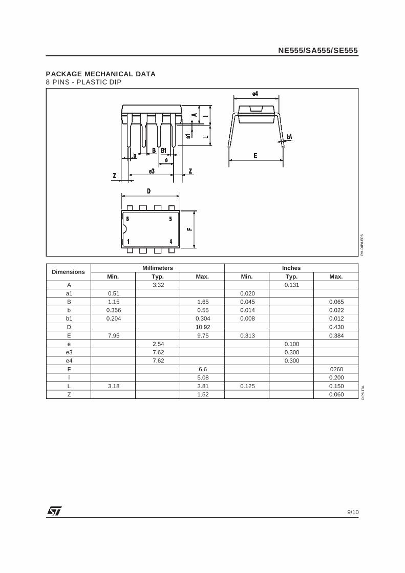
PACKAGE MECHANICAL DATA8 PINS - PLASTIC DIP
DimensionsMillimeters Inches
Min. Typ. Max. Min. Typ. Max.A 3.32 0.131a1 0.51 0.020B 1.15 1.65 0.045 0.065b 0.356 0.55 0.014 0.022
b1 0.204 0.304 0.008 0.012D 10.92 0.430E 7.95 9.75 0.313 0.384e 2.54 0.100
e3 7.62 0.300e4 7.62 0.300F 6.6 0260i 5.08 0.200L 3.18 3.81 0.125 0.150Z 1.52 0.060
DIP
8.T
BL
NE555/SA555/SE555
9/10
PM
-SO
8.E
PS
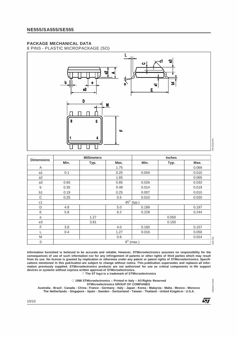
PACKAGE MECHANICAL DATA8 PINS - PLASTIC MICROPACKAGE (SO)
DimensionsMillimeters Inches
Min. Typ. Max. Min. Typ. Max.A 1.75 0.069a1 0.1 0.25 0.004 0.010a2 1.65 0.065a3 0.65 0.85 0.026 0.033b 0.35 0.48 0.014 0.019
b1 0.19 0.25 0.007 0.010C 0.25 0.5 0.010 0.020c1 45o (typ.)D 4.8 5.0 0.189 0.197E 5.8 6.2 0.228 0.244e 1.27 0.050
e3 3.81 0.150F 3.8 4.0 0.150 0.157L 0.4 1.27 0.016 0.050M 0.6 0.024S 8o (max.)
SO
8.TB
L
Information furnished is believed to be accurate and reliable. However, STMicroelectronics assumes no responsibility for theconsequences of use of such information nor for any infringement of patents or other rights of third parties which may resultfrom its use. No license is granted by implication or otherwise under any patent or patent rights of STMicroelectronics. Specif i-cations mentioned in this publication are subject to change without notice. This publication supersedes and replaces all infor-mation previously supplied. STMicroelectronics products are not authorized for use as critical components in life supportdevices or systems without express written approval of STMicroelectronics.
© The ST logo is a trademark of STMicroelectronics
© 1998 STMicroelectronics – Printed in Italy – All Rights ReservedSTMicroelectronics GROUP OF COMPANIES
Australia - Brazil - Canada - China - France - Germany - Italy - Japan - Korea - Malaysia - Malta - Mexico - MoroccoThe Netherlands - Singapore - Spain - Sweden - Switzerland - Taiwan - Thailand - United Kingdom - U.S.A. O
RD
ER
CO
DE
:
NE555/SA555/SE555
10/10

This datasheet has been download from:
www.datasheetcatalog.com
Datasheets for electronics components.
July 1998
NDIP8
(Plastic Package)
DSO8
(Plastic Micropackage)
1
2
3
4 5
6
7
8 1 - GND2 - Trigger3 - Output4 - Reset5 - Control voltage6 - Threshold7 - Discharge8 - VCC
PIN CONNECTIONS (top view)
. LOW TURN OFF TIME.MAXIMUM OPERATING FREQUENCYGREATER THAN 500kHz. TIMING FROM MICROSECONDS TO HOURS.OPERATES IN BOTH ASTABLE ANDMONOSTABLE MODES.HIGH OUTPUT CURRENT CAN SOURCE ORSINK 200mA.ADJUSTABLE DUTY CYCLE. TTL COMPATIBLE. TEMPERATURE STABILITY OF 0.005%PERoC
ORDER CODES
PartNumber
TemperatureRange
Package
N D
NE555 0oC, 70oC • •SA555 –40oC, 105oC • •SE555 –55oC, 125oC • •
DESCRIPTION
The NE555monolithic timing circuit isa highlystablecontrollercapableofproducingaccuratetime delaysor oscillation. In the time delay mode of operation,the time is precisely controlled by one external re-sistorandcapacitor.For astableoperationasanos-cillator, the free running frequency and the duty cy-cle are both accurately controlled with two externalresistors and one capacitor. The circuit may be trig-gered and reset on falling waveforms, and the out-put structure can source or sink up to 200mA. TheNE555 is available in plastic and ceramic minidippackageand in a 8-lead micropackage and in metalcan package version.
NE555SA555 - SE555
GENERAL PURPOSE SINGLE BIPOLAR TIMERS
1/10

THRESHOLD
COMP
5kΩ
5kΩ
5kΩ
TRIGGER
R
FLIP-FLOP
S
Q
DISCHARGE
OUT
INHIBIT/
RESET
RESET
COMP
S - 8086
S
+
CONTROL VOLTAGE
VCC
BLOCK DIAGRAM
OUTPUT
CONTROLVOLTAGE
THRESHOLDCOMPARATOR
VCC
R14.7kΩ
R2830Ω
Q5 Q6 Q7 Q8 Q9
R34.7kΩ
R41kΩ
R85kΩ
Q1
Q2 Q3
Q4
Q10
Q11 Q12
Q13
THRESHOLD
TRIGGER
RES ET
DISCHARGE
G N D
2
4
7
1
Q14
Q15
R510kΩ
R6100kΩ
R7100kΩ
R105kΩ
Q17
Q16 Q18
R95kΩ D2
R16100Ω
R154.7kΩ
R14220Ω
Q24
Q23
R174.7kΩ
3
Q22
Ρ13
D1
Q19Q20
Q21
R126.8kΩ
5
TRIGGER COMPARATOR FLIP FLOP
R115kΩ
3.9kΩ
SCHEMATIC DIAGRAM
ABSOLUTE MAXIMUM RATINGS
Symbol Parameter Value Unit
Vcc Supply Voltage 18 V
Toper Operating Free Air Temperature Range for NE555for SA555for SE555
0 to 70–40 to 105–55 to 125
oC
Tj Junction Temperature 150 oC
Tstg Storage Temperature Range –65 to 150 oC
NE555/SA555/SE555
2/10
ELECTRICAL CHARACTERISTICSTamb = +25oC, VCC = +5V to +15V (unless otherwise specified)
Symbol ParameterSE555 NE555 - SA555
UnitMin. Typ. Max. Min. Typ. Max.
ICC Supply Current (RL ∞) (- note 1)Low State VCC = +5V
VCC = +15VHigh State VCC = 5V
3102
512
3102
615
mA
Timing Error (monostable)(RA = 2k to 100kΩ, C = 0.1µF)Initial Accuracy - (note 2)Drift with TemperatureDrift with Supply Voltage
0.530
0.05
21000.2
1500.1
3
0.5
%ppm/°C
%/V
Timing Error (astable)(RA, RB = 1kΩ to 100kΩ, C = 0.1µF,VCC = +15V)Initial Accuracy - (note 2)Drift with TemperatureDrift with Supply Voltage
1.590
0.15
2.251500.3
%ppm/°C
%/V
VCL Control Voltage levelVCC = +15VVCC = +5V
9.62.9
103.33
10.43.8
92.6
103.33
114
V
Vth Threshold VoltageVCC = +15VVCC = +5V
9.42.7
103.33
10.64
8.82.4
103.33
11.24.2
V
Ith Threshold Current - (note 3) 0.1 0.25 0.1 0.25 µA
Vtrig Trigger VoltageVCC = +15VVCC = +5V
4.81.45
51.67
5.21.9
4.51.1
51.67
5.62.2
V
Itrig Trigger Current (Vtrig = 0V) 0.5 0.9 0.5 2.0 µA
Vreset Reset Voltage - (note 4) 0.4 0.7 1 0.4 0.7 1 V
Ireset Reset CurrentVreset = +0.4VVreset = 0V
0.10.4
0.41
0.10.4
0.41.5
mA
VOL Low Level Output VoltageVCC = +15V, IO(sink) = 10mA
IO(sink) = 50mAIO(sink) = 100mAIO(sink) = 200mA
VCC = +5V, IO(sink) = 8mAIO(sink) = 5mA
0.10.42
2.50.1
0.05
0.150.52.2
0.250.2
0.10.42
2.50.3
0.25
0.250.752.5
0.40.35
V
VOH High Level Output VoltageVCC = +15V, IO(source) = 200mA
IO(source) = 100mAVCC = +5V, IO(source) = 100mA
133
12.513.33.3
12.752.75
12.513.33.3
V
Notes : 1. Supply current when output is high is typically 1mA less.2. Tested at VCC = +5V and VCC = +15V.3. This will determine the maximum value of RA + RB for +15V operation the max total is R = 20MΩ and for 5V operation
the max total R = 3.5MΩ.
OPERATING CONDITIONS
Symbol Parameter SE555 NE555 - SA555 Unit
VCC Supply Voltage 4.5 to 18 4.5 to 18 V
Vth, Vtrig, Vcl, Vreset Maximum Input Voltage VCC VCC V
NE555/SA555/SE555
3/10
ELECTRICAL CHARACTERISTICS (continued)
Symbol ParameterSE555 NE555 - SA555
UnitMin. Typ. Max. Min. Typ. Max.
Idis (off) Discharge Pin Leakage Current(output high) (Vdis = 10V)
20 100 20 100 nA
Vdis(sat) Discharge pin Saturation Voltage(output low) - (note 5)VCC = +15V, Idis = 15mAVCC = +5V, Idis = 4.5mA
18080
480200
18080
480200
mV
trtf
Output Rise TimeOutput Fall Time
100100
200200
100100
300300
ns
toff Turn off Time - (note 6) (Vreset = VCC) 0.5 0.5 µsNotes : 5. No protection against excessive Pin 7 current is necessary, providing the package dissipation rating will not be exceeded.
6. Time mesaured from a positive going input pulse from 0 to 0.8x VCC into the threshold to the drop from high to low of theoutput trigger is tied to treshold.
Figure 1 : Minimum Pulse Width Required forTrigering
Figure 2 : Supply Current versus SupplyVoltage
Figure 3 : Delay Time versus Temperature Figure 4 : Low Output Voltage versus OutputSink Current
NE555/SA555/SE555
4/10
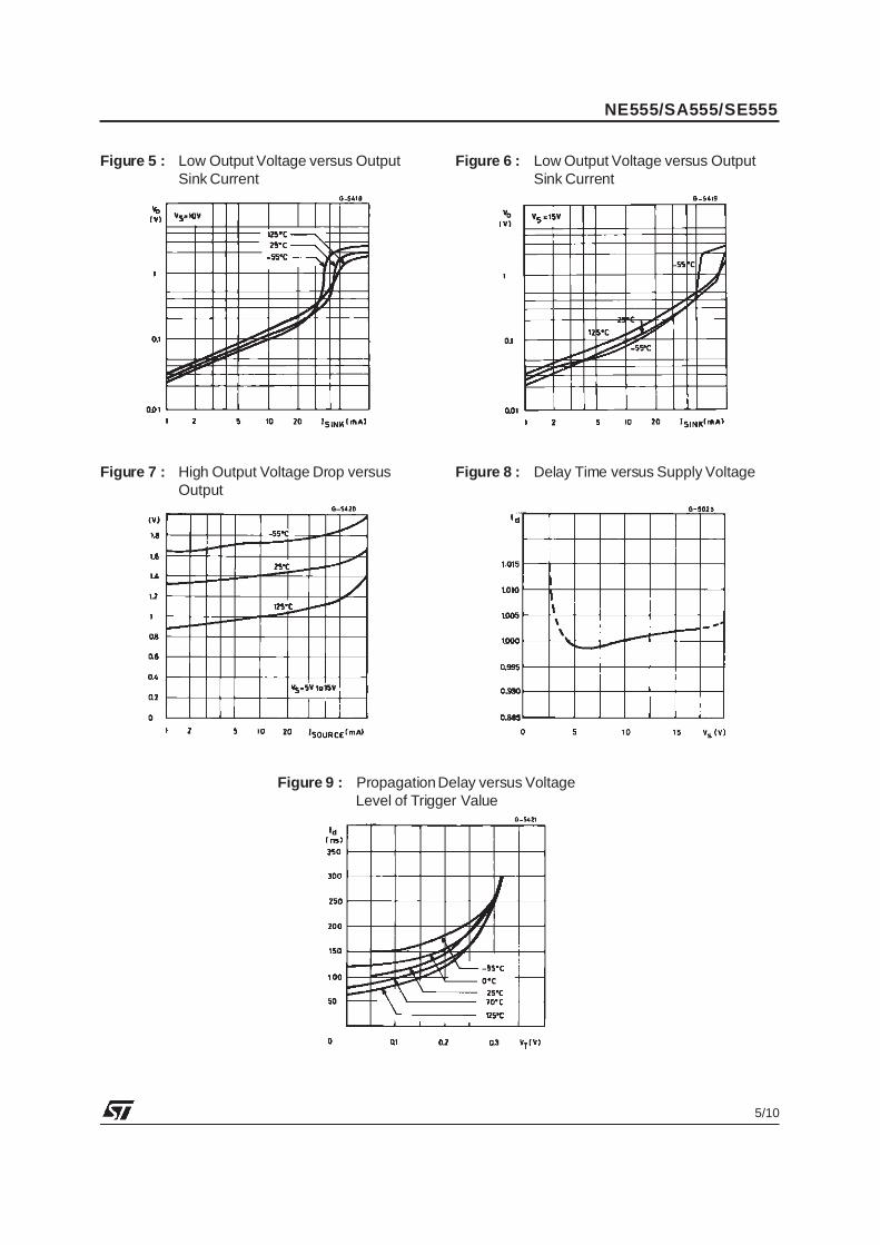
Figure 5 : Low Output Voltage versus OutputSink Current
Figure 6 : Low Output Voltage versus OutputSink Current
Figure 7 : High Output Voltage Drop versusOutput
Figure 8 : Delay Time versus Supply Voltage
Figure 9 : PropagationDelay versus VoltageLevel of Trigger Value
NE555/SA555/SE555
5/10
CAPACITOR VOLTAGE = 2.0V/div
t = 0.1 ms / div
INPUT = 2.0V/div
OUTPUT VOLTAGE = 5.0V/div
R1 = 9.1kΩ, C1 = 0.01µF, R = 1kΩL
Figure 11
Reset
Trigger
Output
R1
C1
Control Voltage
0.01µF
NE555
= 5 to 15VVCC
4
2
3
1
5
6
7
8
Figure 10
C(µF)10
1.0
0.1
0.01
0.00110 100 1.0 10 100 10 (t )dµs µs ms ms ms s
10M
Ω1MΩ10
0kΩ10
kΩR1=1k
Ω
Figure 12
APPLICATION INFORMATION
MONOSTABLE OPERATIONIn the monostable mode, the timer functions as aone-shot.Referring to figure 10 the external capaci-tor is initially held discharged by a transistor insidethe timer.
The circuit triggers on a negative-going input signalwhen the level reaches1/3 Vcc. Once triggered, thecircuit remains in this state until the set time haselapsed, even if it is triggered again during this in-terval.The durationof theoutput HIGHstateisgivenby t = 1.1 R1C1 and is easily determined byfigure 12.Notice that since the charge rate and the thresholdlevelof the comparatorarebothdirectly proportionalto supply voltage, the timing interval is independentof supply. Applying a negativepulse simultaneouslyto the reset terminal (pin 4) and the trigger terminal(pin 2) during the timing cycle discharges the exter-nalcapacitorand causes the cycle to start over.Thetiming cycle now starts on the positive edge of thereset pulse. During the time the reset pulse in ap-plied, the output is driven to its LOW state.When a negativetriggerpulse is applied topin 2, theflip-flop is set, releasing the short circuit across theexternalcapacitor anddriving the output HIGH. Thevoltage across the capacitor increases exponen-tially with the time constantτ =R1C1. When the volt-age across the capacitor equals2/3 Vcc, the compa-ratorresets the flip-flop which thendischarge the ca-pacitor rapidly and drivers the output to its LOWstate.Figure 11shows the actual waveforms generatedinthis mode of operation.When Reset is not used, it should be tied high toavoid any possibly or false triggering.
ASTABLE OPERATIONWhen the circuit is connected as shown in figure 13(pin 2and 6 connected)it triggers itself and freerunsas a multivibrator. The external capacitor chargesthrough R1 and R2 and discharges through R2 only.Thus the duty cycle may beprecisely set by the ratioof these two resistors.In the astable mode of operation, C1 charges anddischarges between 1/3 Vcc and 2/3 Vcc. As in thetriggeredmode, thechargeanddischarge timesandtherefore frequency are independentof the supplyvoltage.
NE555/SA555/SE555
6/10
t = 0.5 ms / div
OUTPUT VOLTAGE = 5.0V/div
CAPACITOR VOLTAGE = 1.0V/div
R1 = R2 = 4.8kΩ, C1= 0.1µF, R = 1kΩL
Figure 14
C(µF)10
1.0
0.1
0.01
0.0010.1 1 10 100 1k 10k f (Hz)o
1MΩ
R1 + R2= 10MΩ
100kΩ
10kΩ
1kΩ
Figure 15 : Free Running Frequency versus R1,R2 and C1
Figure 14showsactualwaveforms generatedin thismode of operation.The charge time (output HIGH) is given by :t1 = 0.693 (R1 + R2) C1
and the discharge time (output LOW) by :t2 = 0.693 (R2) C1
Thus the total period T is given by :T = t1 + t2 = 0.693 (R1 + 2R2) C1
The frequency ofoscillation is them :
f = 1T
= 1.44(R1 + 2R2) C1
and may be easily found by figure 15.The duty cycle is given by :
D = R2
R1 + 2R2
Output 3
4 8
7
5
1
R1
C12
6
R2
ControlVoltage
NE555
VCC = 5 to 15V
0.01µF
Figure 13
PULSE WIDTH MODULATORWhen the timer is connected in the monostablemode and triggered with a continuous pulse train,the output pulse width can be modulatedby a signalapplied to pin 5. Figure 16 shows the circuit.
Trigger
Output
R
C
NE555
2
4
3
1
5
6
7
ModulationInput
8
A
VCC
Figure 16 : Pulse Width Modulator.
NE555/SA555/SE555
7/10
LINEAR RAMPWhen the pullup resistor, RA, in the monostable cir-cuit is replacedby a constantcurrent source,a linearramp is generated. Figure 17 shows a circuit con-figuration that will perform this function.
Trigger
Output
C
NE555
2
4
3
1
5
6
7
8
E
VCC
0.01µFR2
R1R
2N4250or equiv.
Figure 17.
Out
R A
C
NE55
2
4
3
1
5
6
7
8
VCC
51kΩ
RB
22kΩ
0.01µF
VCC
0.01µF
Figure 19 : 50%Duty Cycle Oscillator.
Figure 18 shows waveformsgeneratorby the linearramp.The time interval is given by :
T = (2/3 VCC RE (R1+ R2) CR1 VCC − VBE (R1+ R2)
VBE = 0.6V
Figure 18 : Linear Ramp.
VCC = 5V Top trace : input 3V/DIVTime = 20µs/DIV Middle trace : output 5V/DIVR1 = 47kΩ Bottom trace : output 5V/DIVR2 = 100kΩ Bottom trace : capacitor voltageRE = 2.7kΩ 1V/DIVC = 0.01µF
50% DUTY CYCLE OSCILLATORFor a 50% duty cycle the resistors RA and RE maybeconnectedas in figure19. The time preriod for theoutput high is the same as previous,t1 = 0.693 RA C.For the output low it is t2 =
[(RARB) ⁄ (RA + RB)] CLn
RB − 2RA
2RB − RA
Thus the frequencyof oscillation is f = 1t1 + t2
Note that this circuit will not oscillate if RB is greater
than 1/2 RA because the junction of RA and RB can-not bring pin2 down to 1/3 VCC andtrigger the lowercomparator.
ADDITIONAL INFORMATIONAdequate power supply bypassing is necessary toprotect associated circuitry. Minimum recom-mended is 0.1µF in parallel with 1µF electrolytic.
NE555/SA555/SE555
8/10
PM
-DIP
8.E
PS
PACKAGE MECHANICAL DATA8 PINS - PLASTIC DIP
DimensionsMillimeters Inches
Min. Typ. Max. Min. Typ. Max.A 3.32 0.131
a1 0.51 0.020B 1.15 1.65 0.045 0.065b 0.356 0.55 0.014 0.022b1 0.204 0.304 0.008 0.012
D 10.92 0.430
E 7.95 9.75 0.313 0.384e 2.54 0.100e3 7.62 0.300e4 7.62 0.300
F 6.6 0260i 5.08 0.200
L 3.18 3.81 0.125 0.150Z 1.52 0.060
DIP
8.T
BL
NE555/SA555/SE555
9/10
PM
-SO
8.E
PS
PACKAGE MECHANICAL DATA8 PINS - PLASTIC MICROPACKAGE (SO)
DimensionsMillimeters Inches
Min. Typ. Max. Min. Typ. Max.A 1.75 0.069
a1 0.1 0.25 0.004 0.010a2 1.65 0.065a3 0.65 0.85 0.026 0.033b 0.35 0.48 0.014 0.019
b1 0.19 0.25 0.007 0.010
C 0.25 0.5 0.010 0.020c1 45o (typ.)D 4.8 5.0 0.189 0.197E 5.8 6.2 0.228 0.244
e 1.27 0.050e3 3.81 0.150
F 3.8 4.0 0.150 0.157L 0.4 1.27 0.016 0.050M 0.6 0.024
S 8o (max.)
SO
8.T
BL
Information furnished is believed to be accurate and reliable. However, STMicroelectronics assumes no responsibility for theconsequences of use of such information nor for any infringement of patents or other rights of third parties which may resultfrom its use. No license is granted by implication or otherwise under any patent or patent rights of STMicroelectronics. Specifi-cations mentioned in this publication are subject to change without notice. This publication supersedes and replaces all infor-mation previously supplied. STMicroelectronics products are not authorized for use as critical components in life supportdevices or systems without express written approval of STMicroelectronics.
The ST logo is a trademark of STMicroelectronics
1998 STMicroelectronics – Printed in Italy – All Rights ReservedSTMicroelectronics GROUP OF COMPANIES
Australia - Brazil - Canada - China - France - Germany - Italy - Japan - Korea - Malaysia - Malta - Mexico - MoroccoThe Netherlands - Singapore - Spain - Sweden - Switzerland - Taiwan - Thailand - United Kingdo m- U.S.A. O
RD
ER
CO
DE
:
NE555/SA555/SE555
10/10

This datasheet has been download from:
www.datasheetcatalog.com
Datasheets for electronics components.