Field Effect Transistors with Organic Semiconductor Layers Assembled from Aqueous Colloidal...
7
Field Effect Transistors with Organic Semiconductor Layers Assembled from Aqueous Colloidal Nanocomposites Chiara Dionigi,* ,² Pablo Stoliar,* ,² William Porzio, ‡ Silvia Destri, ‡ Massimiliano Cavallini, ² Ivano Bilotti, § Aldo Brillante, § and Fabio Biscarini ² Istituto per lo Studio dei Materiali Nanostrutturati, Consiglio Nazionale delle Ricerche, Via P. Gobetti 101, I-40129 Bologna, Istituto per lo Studio delle Macromolecole, Consiglio Nazionale delle Ricerche, Via Bassini 15, I-20133 Milano, and Dipartimento di Chimica Fisica e Inorganica and INSTM-UdR Bologna, UniVersity of Bologna, Viale Risorgimento 4, I-40136, Bologna, Italy ReceiVed August 10, 2006. In Final Form: October 16, 2006 We demonstrate field effect transistors based on organic semiconductor molecules dispersed in a self-organized polystyrene (PS) latex bead matrix. An aqueous colloidal composite made of PS and tetrahexylsexithiophene (H4T6) is deposited with a micropipet into the channel of a bottom-contact field effect transistor. The beads self-organize into a network whose characteristic distances are governed by their packing. The semiconductor molecules crystallize in the interstitial voids, leading to the growth of large interconnected domains. Depending on the bead size and the ratio between H4T6 and PS, the fraction of the different phases in the polymorph can be controlled. In the transistors where the H4T6 metastable “red phase” is the largest, the device response and the charge mobility are comparable to those of sexithienyl thin films grown by high-vacuum sublimation. Introduction Organic semiconductors are materials of great interest for the development of novel electronics devices, such as field effect transistors (FETs), diodes, and photovoltaic junctions. The charge transport layer in such devices consists of a thin film of conjugated polymers or molecules. Polymer semiconductor thin films are deposited from solution by spin coating or patterned by ink-jet printing. 1 Conjugated molecules are mostly processed by high- vacuum sublimation. 2-4 Molecular materials exhibit larger charge mobility values, because of the enhanced molecular order in the transport channel; hence, they are more attractive for FETs. 5,6 Charge transport is correlated to the morphology of the active layer at length scales larger than the molecular ones. This was shown clearly in the case of high-vacuum sublimed oligomers. 3 Controlling the molecular order at length scales comparable to the channel length of the device is extremely difficult for any established thin film technology. 7-9 An attractive possibility consists of exploiting self-organization at all length scales. This can be pursued with materials, for instance semiconductor discotic liquid crystals, where cooperativity is built into the design of the material. 10 Recently, it was demonstrated by means of a combined fluidics/printing deposition of bilayer stripes that the charge mobility of self-organized nanostructures is two orders of magnitude larger with respect to that of the corresponding spin-cast material. 11 This is the result of the better control in time and in space of supersaturation and precipitation in confined environments, which leads to the self- organization of the molecular semiconductor into very large molecularly ordered and oriented domains. In this paper, we present a “chimie douce” approach to form organic semiconductor layers with enhanced charge transport properties in organic FETs. Our process relies on the self- organization of the semiconductor molecules, viz., tetrahexyl- * To whom correspondence should be addressed. E-mail: c.dionigi@ bo.ismn.cnr.it (C.D.); [email protected] (P.S.). ² Istituto per lo Studio dei Materiali Nanostrutturati, Consiglio Nazionale delle Ricerche. ‡ Istituto per lo Studio delle Macromolecole, Consiglio Nazionale delle Ricerche. § University of Bologna. (1) Horowitz, G. J. Mater. Res. 2004, 19, 1946. (2) Dimitrakopoulos, C. D.; Malenfant, P. R. L. AdV. Mater. 2002, 14, 99. (3) Dinelli, F.; Murgia, M.; Levy, P.; Cavallini, M.; Biscarini, F.; de Leeuw, D. M. Phys. ReV. Lett. 2004, 92, 116802. (4) Stallinga, P.; Gomes, H. L.; Biscarini, F.; Murgia, M.; de Leeuw, D. M. J. Appl. Phys. 2004, 96, 5277. (5) Videlot, C.; Ackermann, J.; Blanchard, P.; Raimundo, J.-M.; Fre `re, P.; Allain, M.; de Bettignies, R.; Levillain, E.; Roncali, J. AdV. Mater. 2003, 15, 306. (6) Alik, M.; Klauk, H.; Zschieschang, U.; Schmid, G.; Ponomarenko, S.; Kirchmeyer, S.; Weber, W. AdV. Mater. 2003, 15, 917. (7) De Boer, R. W. I.; Gershenson, M. E.; Morpurgo, A. F.; Podzorov, V. Phys. Status Solidi A 2004, 201, 1302. (8) Leufgen, M.; Bass, U.; Muck, T.; Borzenko, T.; Schmidt, G.; Geurts, J.; Wagner, V.; Molenkamp, L. W. Synth. Met. 2004 146, 341. (9) Saya, D.; Coleman, A. W.; Lazar, A. N.; Bergaud, C.; Nicu, L. Appl. Phys. Lett. 2005, 87, 103901. (10) Roussel, O.; Kestemont, G.; Tant, J.; De Halleux, V.; Aspe, R. G.; Levin, J.; Remacle, A.; Geerts, Y. Mol. Cryst. Liq. Cryst. 2003, 396, 35. (11) Cavallini, M.; Stoliar, P.; Moulin, J. F.; Surin, M.; Leclere, P.; Lazzaroni, R.; Breiby, D. W.; Andreasen, J. W.; Nielsen, M. M.; Sonar, P.; Grimsdale, A. C.; Mullen, K.; Biscarini, F. Nano Lett. 2005, 5, 2422. Figure 1. Scheme of the H4T6 molecular structure. 2030 Langmuir 2007, 23, 2030-2036 10.1021/la062371k CCC: $37.00 © 2007 American Chemical Society Published on Web 12/14/2006
Transcript of Field Effect Transistors with Organic Semiconductor Layers Assembled from Aqueous Colloidal...
Field Effect Transistors with Organic Semiconductor LayersAssembled from Aqueous Colloidal Nanocomposites
Chiara Dionigi,*,† Pablo Stoliar,*,† William Porzio,‡ Silvia Destri,‡ Massimiliano Cavallini,†Ivano Bilotti,§ Aldo Brillante,§ and Fabio Biscarini†
Istituto per lo Studio dei Materiali Nanostrutturati, Consiglio Nazionale delle Ricerche, Via P. Gobetti101, I-40129 Bologna, Istituto per lo Studio delle Macromolecole, Consiglio Nazionale delle Ricerche, ViaBassini 15, I-20133 Milano, and Dipartimento di Chimica Fisica e Inorganica and INSTM-UdR Bologna,
UniVersity of Bologna, Viale Risorgimento 4, I-40136, Bologna, Italy
ReceiVed August 10, 2006. In Final Form: October 16, 2006
We demonstrate field effect transistors based on organic semiconductor molecules dispersed in a self-organizedpolystyrene (PS) latex bead matrix. An aqueous colloidal composite made of PS and tetrahexylsexithiophene (H4T6)is deposited with a micropipet into the channel of a bottom-contact field effect transistor. The beads self-organizeinto a network whose characteristic distances are governed by their packing. The semiconductor molecules crystallizein the interstitial voids, leading to the growth of large interconnected domains. Depending on the bead size and theratio between H4T6 and PS, the fraction of the different phases in the polymorph can be controlled. In the transistorswhere the H4T6 metastable “red phase” is the largest, the device response and the charge mobility are comparableto those of sexithienyl thin films grown by high-vacuum sublimation.
Introduction
Organic semiconductors are materials of great interest for thedevelopment of novel electronics devices, such as field effecttransistors (FETs), diodes, and photovoltaic junctions. The chargetransport layer in such devices consists of a thin film of conjugatedpolymers or molecules. Polymer semiconductor thin films aredeposited from solution by spin coating or patterned by ink-jetprinting.1 Conjugated molecules are mostly processed by high-vacuum sublimation.2-4Molecular materials exhibit larger chargemobility values, because of the enhanced molecular order in thetransport channel; hence, they are more attractive for FETs.5,6
Charge transport is correlated to the morphology of the activelayer at length scales larger than the molecular ones. This wasshown clearly in the case of high-vacuum sublimed oligomers.3
Controlling the molecular order at length scales comparable tothe channel length of the device is extremely difficult for anyestablished thin film technology.7-9
An attractive possibility consists of exploiting self-organizationat all length scales. This can be pursued with materials, for instancesemiconductor discotic liquid crystals, where cooperativity is
built into the design of the material.10 Recently, it wasdemonstrated by means of a combined fluidics/printing depositionof bilayer stripes that the charge mobility of self-organizednanostructures is two orders of magnitude larger with respect tothat of the corresponding spin-cast material.11 This is the resultof the better control in time and in space of supersaturation andprecipitation in confined environments, which leads to the self-organization of the molecular semiconductor into very largemolecularly ordered and oriented domains.
In this paper, we present a “chimie douce” approach to formorganic semiconductor layers with enhanced charge transportproperties in organic FETs. Our process relies on the self-organization of the semiconductor molecules, viz., tetrahexyl-
* To whom correspondence should be addressed. E-mail: [email protected] (C.D.); [email protected] (P.S.).
† Istituto per lo Studio dei Materiali Nanostrutturati, Consiglio Nazionaledelle Ricerche.
‡ Istituto per lo Studio delle Macromolecole, Consiglio Nazionale delleRicerche.
§ University of Bologna.(1) Horowitz, G.J. Mater. Res.2004, 19, 1946.(2) Dimitrakopoulos, C. D.; Malenfant, P. R. L.AdV. Mater. 2002, 14, 99.(3) Dinelli, F.; Murgia, M.; Levy, P.; Cavallini, M.; Biscarini, F.; de Leeuw,
D. M. Phys. ReV. Lett. 2004, 92, 116802.(4) Stallinga, P.; Gomes, H. L.; Biscarini, F.; Murgia, M.; de Leeuw, D. M.
J. Appl. Phys.2004, 96, 5277.(5) Videlot, C.; Ackermann, J.; Blanchard, P.; Raimundo, J.-M.; Fre`re, P.;
Allain, M.; de Bettignies, R.; Levillain, E.; Roncali, J.AdV. Mater.2003, 15, 306.(6) Alik, M.; Klauk, H.; Zschieschang, U.; Schmid, G.; Ponomarenko, S.;
Kirchmeyer, S.; Weber, W.AdV. Mater. 2003, 15, 917.(7) De Boer, R. W. I.; Gershenson, M. E.; Morpurgo, A. F.; Podzorov, V.
Phys. Status Solidi A2004, 201, 1302.(8) Leufgen, M.; Bass, U.; Muck, T.; Borzenko, T.; Schmidt, G.; Geurts, J.;
Wagner, V.; Molenkamp, L. W.Synth. Met.2004146, 341.(9) Saya, D.; Coleman, A. W.; Lazar, A. N.; Bergaud, C.; Nicu, L.Appl. Phys.
Lett. 2005, 87, 103901.
(10) Roussel, O.; Kestemont, G.; Tant, J.; De Halleux, V.; Aspe, R. G.; Levin,J.; Remacle, A.; Geerts, Y.Mol. Cryst. Liq. Cryst.2003, 396, 35.
(11) Cavallini, M.; Stoliar, P.; Moulin, J. F.; Surin, M.; Leclere, P.; Lazzaroni,R.; Breiby, D. W.; Andreasen, J. W.; Nielsen, M. M.; Sonar, P.; Grimsdale,A. C.; Mullen, K.; Biscarini, F.Nano Lett.2005, 5, 2422.
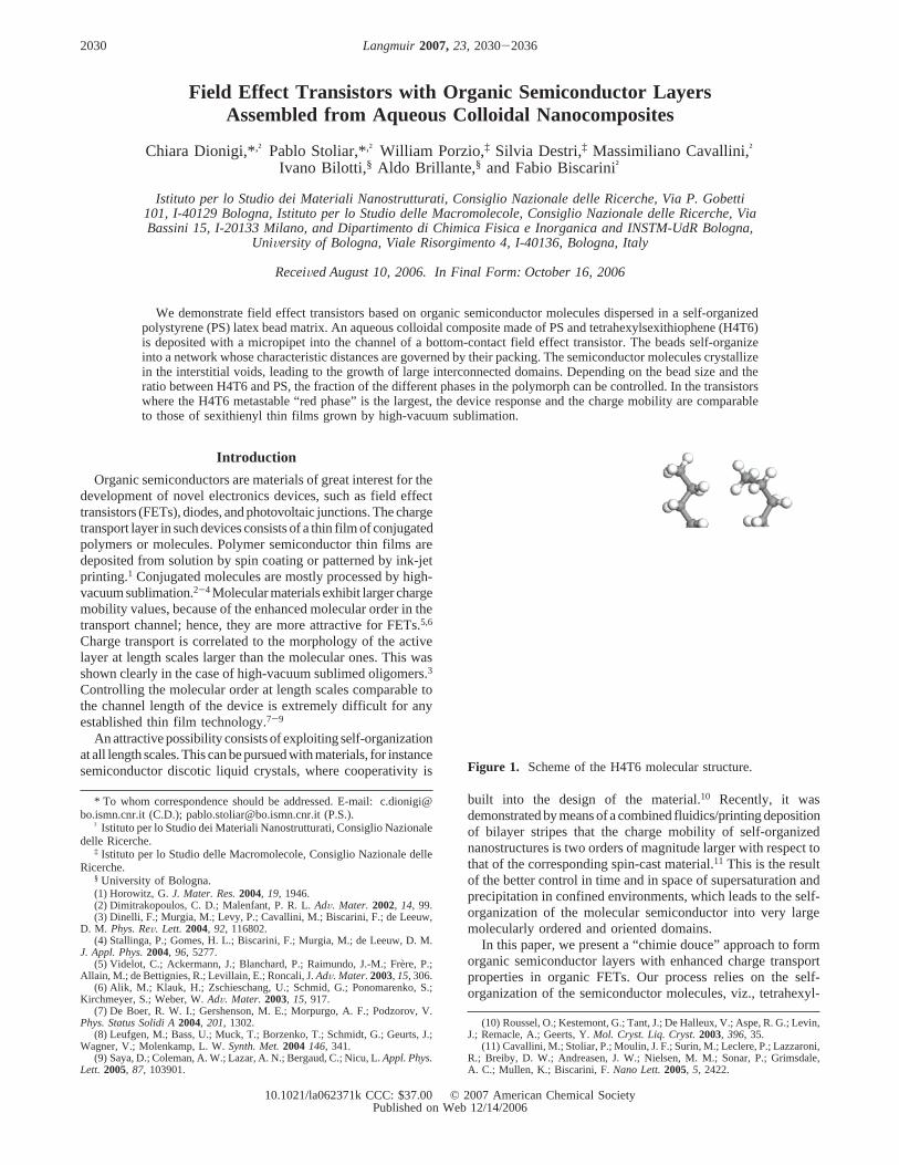
Figure 1. Scheme of the H4T6 molecular structure.
2030 Langmuir2007,23, 2030-2036
10.1021/la062371k CCC: $37.00 © 2007 American Chemical SocietyPublished on Web 12/14/2006
sexithiophene (H4T6),12-16 in a confined environment definedby the assembly of mesoscopic polystyrene beads, hereafter calledPS, decorated with H4T6. The decorated beads are cast in thechannel of field effect transistors at ambient conditions. H4T6molecules are slowly released on the dielectric surface of thetransistor channel, and crystalline domains grow in the interstitialcavities. The mesoscopic and nanoscale channels in the templatedictate the length and time scales for the deposition and nucleation.These devices exhibit a charge mobility of 10-3 cm2/(V s), viz.,1 order of magnitude lower than that of high-vacuum grownsexithienyl thin films,3,4 a threshold voltage close to 0 V, a sub-threshold slope of 0.2 V/decade, and on/off ratios in excess of102. The enhanced device response is correlated to the dominanceof two polymorphs (red (R) and meso (M) phases) by means ofX-ray diffraction (XRD) and confocal Raman spectroscopy.
Experimental Section
Decoration of PS with H4T6. Syntheses of both monodispersePS and H4T6 are reported elsewhere.13,17
H4T6 is a semiconductive oligomer stable in the solid phaseunder ambient conditions (see Figure 1); it is insoluble in water,
(12) Botta, C.; Destri, S.; Porzio, W.; Bongiovanni, G.; Loi, M. A.; Mura, A.;Tubino, R.Synth. Met.2001, 122, 395.
(13) Destri, S.; Ferro, D. R.; Khotina, I. A.; Porzio, W.; Farina, A.Macromol.Chem. Phys.1998, 199, 1973.
(14) Borghesi, A.; Sassella, A.; Tubino, R.; Destri, S.; Porzio, W.AdV. Mater.1998, 10, 931.
(15) Porzio, W.; Giovanella, U.; Botta, C.; Pasini, M.; Destri, S.; Provasi, C.;Rossi, V.Org. Electron.2004, 5, 59.
(16) Botta, C.; Destri, S.; Porzio, W.; Sassella, A.; Borghesi, A.; Tubino, R.Opt. Mater.1999, 12, 301.
(17) Dionigi, C.; Nozar, P.; Di Domenico, D.; Calestani, G.J. Colloid InterfaceSci.2004, 275, 445.
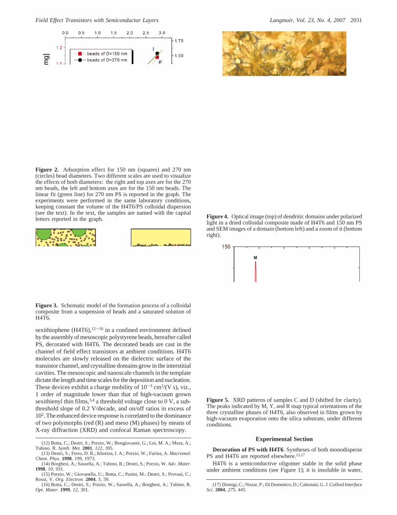
Figure 2. Adsorption effect for 150 nm (squares) and 270 nm(circles) bead diameters. Two different scales are used to visualizethe effects of both diameters: the right and top axes are for the 270nm beads, the left and bottom axes are for the 150 nm beads. Thelinear fit (green line) for 270 nm PS is reported in the graph. Theexperiments were performed in the same laboratory conditions,keeping constant the volume of the H4T6/PS colloidal dispersion(see the text). In the text, the samples are named with the capitalletters reported in the graph.
Figure 3. Schematic model of the formation process of a colloidalcomposite from a suspension of beads and a saturated solution ofH4T6.
Figure 4. Optical image (top) of dendritic domains under polarizedlight in a dried colloidal composite made of H4T6 and 150 nm PSand SEM images of a domain (bottom left) and a zoom of it (bottomright).
Figure 5. XRD patterns of samples C and D (shifted for clarity).The peaks indicated by M, Y, and R map typical orientations of thethree crystalline phases of H4T6, also observed in films grown byhigh-vacuum evaporation onto the silica substrate, under differentconditions.
Field Effect Transistors with Semiconductor Layers Langmuir, Vol. 23, No. 4, 20072031
partially soluble in ethanol (∼0.5 mg/mL), and totally soluble inorganic solvents such as acetone.
In our work, the bead decoration is driven by highly hydrophobicinteractions between H4T6 and polymeric nanobeads in a hydrophilicmedium.
When an acetone/ethanol solution of H4T6 is mixed with water,H4T6 starts to nucleate. We found that a precise water/organic ratiois able to induce the nucleation of H4T6 into clusters that make theliquid phase opaque.
PS decoration was performed by mixing 10 mg of H4T6(previously dissolved in 4 mL of acetone/ethanol (1:3) by volume)with 20 mL of an aqueous PS dispersion containing 20 mg of PS(D ) 150 ( 4 nm,D ) 270 ( 7 nm). The final solvent mixtureresulted in a 5:1 (v/v) water:organic solvent ratio. H4T6 clusterswere collected by polymeric nanobeads, and a homogeneous colloidalsuspension of decorated beads was formed.
Photon correlation spectroscopy (PCS) analysis andZ-potentialmeasurements confirmed the adsorption of H4T6 on the nanobeads,as a decrease in both the external nanobead charge and hydrodynamicdiameter was observed.
Decorated beads were separated from the liquid phase bycentrifugation at 700-3000g acceleration. The dry supernatant wasdissolved in acetone and analyzed by spectrophotometry atλ ) 411nm, to estimate the amount of adsorbed H4T6.
The wet deposit spontaneously dispersed as a highly viscouscolloidal suspension of the H4T6-decorated beads. A total of 58%
of the starting H4T6 was contained in the surnatant liquid phase,while 42% remained in the viscous phase, whose volume is 10%of the total volume. These proportions are highly reproducible.
Preparation of Transistors. The FET test patterns were givenby Philips Research Laboratories (courtesy of Dr. D. de Leeuw).These are prepared on top of a heavily n-type-doped silicon substrate,acting as a gate, with a 200 nm thick thermally grown SiO2 insulatinglayer which is primed with hexamethyldisilazane (HMDS). Theinsulating layer has a capacitance per area unit of 17 nF/cm2. Twointerdigitated 150 nm thick evaporated gold pads on a Ti adhesionlayer form the drain and source contacts and define a transistorchannel 10µm long and 10 mm wide. Before the deposition, the testpattern was cleaned by using boiling acetone and then acetone vaporand immediately dried by using filtered dry nitrogen.
A drop of approximately 1µL was deposited on top of each testpattern with a tapered glass micropipet. After drying, a semisphericaldeposit a few hundred micrometers thick was formed, completelycovering the test pattern. In the case of incomplete coverage, thechannel width value has to be properly corrected.
XRD Measurements. Room-temperature XRD measurementswere performed in Bragg-Brentano geometry using a Siemens D-500apparatus equipped with Soller slits and narrow windows (0.3°/0.15°). Cu KR radiation at 40 kV× 40 mA power was used.
Raman Measurements. Raman spectra were recorded with theJobin Yvon spectrometers T64000 (excitation from a Kr laser, 647.1nm) and LABRAM (excitation from a He/Ne laser, 632.8 nm). The
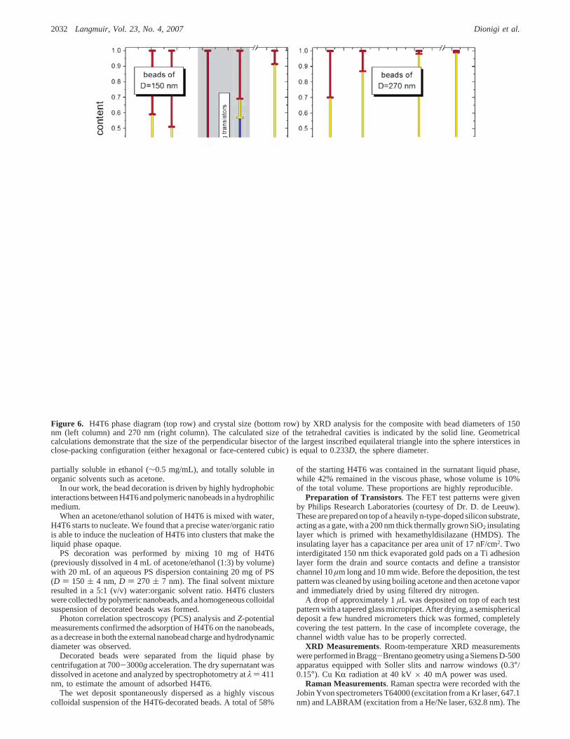
Figure 6. H4T6 phase diagram (top row) and crystal size (bottom row) by XRD analysis for the composite with bead diameters of 150nm (left column) and 270 nm (right column). The calculated size of the tetrahedral cavities is indicated by the solid line. Geometricalcalculations demonstrate that the size of the perpendicular bisector of the largest inscribed equilateral triangle into the sphere interstices inclose-packing configuration (either hexagonal or face-centered cubic) is equal to 0.233D, the sphere diameter.
2032 Langmuir, Vol. 23, No. 4, 2007 Dionigi et al.
laser output power focused on the sample was reduced with a neutralfilter, whose optical density was selected in each experiment toavoid phase transformation (yellow (Y) to R) produced by heating.A confocal optical microscope (Olympus BX40) was interfaced tothe spectrometers, and 50× or 100× objectives were used. Thespatial resolution, given by the laser spot area, ranged from 0.88 to1.05 µm, depending on the numerical aperture of the microscopeobjective and on the wavelength of the laser line. The point to pointvariation of the Raman spectra was obtained by scanning the surface,typically a few tenths of micrometers, with steps as close as 2µm,with an xy motorized stage. Confocal Raman mapping was thenautomatically achieved after selection of the area to be sampled andthe number of points to be measured, their density being chosenaccording to the size of the specimen and the microscope objectiveused.
Theoretical Basis: Measurement of the Transistor Responseand Extraction of the Parameters.The mobility is extracted fromthe transfer characteristicId ) f(Vgs) in the saturation regime (|Vds|> |Vgs - Vt|): µsat ) 2(L/WCi)(dId/dVgs)2, where Id is the draincurrent,WandL are the channel width and length,µsatis the saturatedcharge carrier mobility,Ci is the dielectric layer capacitance per areaunit, Vt is the threshold voltage, andVgs andVds are the gate-sourceand the drain-source potentials. The subthreshold slope, on/off ratio,and threshold voltage shift were extracted from the transfercharacteristic forVds ) -21 V.
The transfer characteristics were measured at ambient conditionsin darkness. The values of the drain current were measured by usinga Keithley 6430 subfemtoammeter, which also was used to polarizethe channel. During the acquisition, a Keithley 3930A multifunctionsynthesizer connected to a homemade voltage amplifier, varyingwith a rate of 100 V/s, supplied the gate voltage.
Results and Discussion
The building blocks are formed upon the effect of highlyhydrophobic interactions18 between H4T6 and PS in an aqueousmedium formed by an acetone/ethanol solution of H4T6 mixedwith water. This process is different from most of the chemicalmethods for core-shell bead synthesis which exploit ionic orpolar interactions.19-24 In these conditions, H4T6 nuclei form inthe solution and then adsorb on PS,25 forming a stable colloidalsuspension.
The relative amount of H4T6 adsorbed on PS depends criticallyon the bead size and the initial H4T6/PS ratio, as shown inFigure 2 for two different bead diameters. The 150 nm beadsexhibit a constant adsorption yield in the range from 20% to 44%by weight of initial H4T6/PS. This evidence is consistent withthe process depicted in Figure 3 where first PS collects H4T6nuclei after mixing of the aqueous PS suspension with the H4T6
(18) Kohut-Svelko, N.; Reynaud, S.; Dedryevre, R.; Martinez, H.; Gonbeau,D.; Francois, J.Langmuir2005, 21, 1575.
(19) Caruso, F.; Lichtenfeld, H.; Giersig, M.; Mo¨hwald, H.J. Am. Chem. Soc.1998, 120, 8523.
(20) Radtchenko, I. L.; Sulkhorukov, G. B.; Gaponik, N.; Kornowski, A.;Rogach, A. L.; Mohwald, H.AdV. Mater. 2001, 13, 1684.
(21) Donath, E.; Sulkhorukov, G. B.; Caruso, F.; Devis, S. A.; Mo¨hwald, H.Angew. Chem., Int. Ed.1998, 37, 2202.
(22) Caruso, F.AdV. Mater. 2001, 13, 11.(23) Jang, J.; Oh, J. H.AdV. Funct. Mater.2005, 15, 494.(24) Khan, M. A.; Armes, S. P.AdV. Mater. 2000, 12, 671.(25) Rigaud, J. L.; Levy, D.; Mosser, G.; Lambert, O.Eur. Biophys. J.1998,
27, 305.
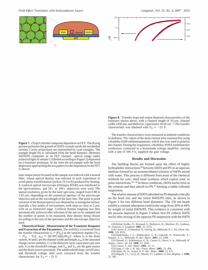
Figure 7. (Top) Colloidal composite deposition on FET. The dryingprocess promotes the growth of H4T6 crystals inside the tetrahedralcavities. Cavity projections are represented by cyan triangles. Thetriangle height (h) is calculated from the bead diameter. (Bottom)H4T6/PS composite as an FET channel: optical image underpolarized light of sample C (labeled according to Figure 2) depositedon a transistor prototype. In the inset the micropipet with the beaddispersion approaching the test pattern for the deposition on the FETis shown.
Figure 8. Transfer (top) and output (bottom) characteristics of thetransistor shown above, with a channel length of 10µm, channelwidth 1450µm, and dielectric capacitance 18 nF cm-2. The transfercharacteristic was obtained withVds ) -21 V.
Field Effect Transistors with Semiconductor Layers Langmuir, Vol. 23, No. 4, 20072033
ethanol/acetone solution and then forms a close-packed structureupon centrifugation. The H4T6 nuclei carried by the beads fillthe cavities, as 26% of the volume in a close-packed structureis empty. This explains the plateau at about 20% in weight (thedensities of the two materials are comparable). Above a criticalinitial H4T6/PS ratio, the available PS surface is insufficient tocollect the excess nuclei, and these coalesce independently ofthe beads. This parasitic flocculation of H4T6 is a competingparallel process that manifests itself in the linear rise of theadsorption curve. For 270 nm beads, the same conditions as for150 nm beads were used, but the linear dependence throughoutthe range suggests that H4T6 infilling of the close-packed beadsis not achieved. In this case, the H4T6 flocculation hinders theinfilling process because of the decreased surface area.
After centrifugation, a wet H4T6/PS deposit is collected. Thisdeposit spontaneously disperses in the residual moisture in theform of a “slurry”, hereafter termed acolloidal composite, whichcontains H4T6 adsorbed on and between the beads.
The colloidal composites of 270 and 150 nm beads were caston silicon oxide substrates with a pipet. Depending on the amountof adsorbed H4T6, the dry deposited film of the colloidalcomposite of 150 nm beads forms large dendritic domains. Thesedomains exhibit birefringence under a polarizing microscope.Domains of the H4T6/PS composite larger than 50µm are visiblein the optical image in Figure 4 (top).
The morphology of the 150 nm deposit is shown in the scanningelectron micrographs (Figure 4 (bottom)). The scanning electronmicroscopy (SEM) images show dendritic domains made of
densely packed beads embedded in an H4T6 matrix. Thebirefringent domains are not observed when films are drop castfrom H4T6 solution without beads or from colloidal compositesmade of larger beads (270, 340, and 415 nm diameter).
XRD patterns on PS/H4T6 composites deposited on glass slides(Figure 5) demonstrate the presence of crystals of H4T6. Thethree phases reported earlier, viz., Y, R, and M phases,12-16 arepresent. The known phases, already present in the dry colloidalcomposite, appear in different proportions depending on boththe size and the amount of PS in the composite, as shown inFigure 6. This is a consequence of the different thermodynamicstabilities of the known phases. The Y phase is the mostthermodynamically stable at room temperature, while the R andM phases are kinetically favored.12-16 The crystallization rate iscontrolled by the evaporation of the liquid phase, whichdetermines the transition from thermodynamic to kinetic control.In the colloidal composite made of 150 nm beads, the volumeof liquid phase infilling the cavities is small and is quicklyevaporated. The deposition is under kinetic control; thus, R andM phases are preferentially formed. In the colloidal compositewith 270 nm beads and a high H4T6/PS ratio, the amount ofliquid in the interstitial space or surrounding the flocculateddeposit is larger and the solvent evaporation process takes placein a longer time. The system is under thermodynamic control,and the Y phase is preferentially formed.
The coherence length of the crystals, viz., the mean domainsize, extracted from analysis of the XRD data, is controlled bythe crystallization inside the interstitial sites as shown in Figure6. There is a clear correlation between the size of the tetrahedralsites in the close-packed structures of the beads26 and thecoherence length of the H4T6 crystals infilled in PS structures,independently of the phase.
Our experimental evidence demonstrates that the compositecomposition, semiconductor crystal phases, crystal size, anddistribution arise from a spontaneous process.
The H4T6/PS composite has been then used to form thetransport layer of an FET device. Colloidal composites made ofH4T6 and PS of diameter sizes of both 150 and 270 nm weredeposited on top of a bottom contact FET transistor test patternas shown in Figure 7.
In the case of H4T6/PS composites made with 150 nm beads,we explored systematically the effect of the amount of H4T6infilled. A clear FET behavior was observed in the condition of“full infilling” of the cavities of the PS close-packed array(samples C and D). Similar electrical characteristics were observedthroughout the range where the adsorbed H4T6/PS concentrationis constant at about 20% by weight. The electrical data demonstrateclearly an excellent reproducibility of the method.
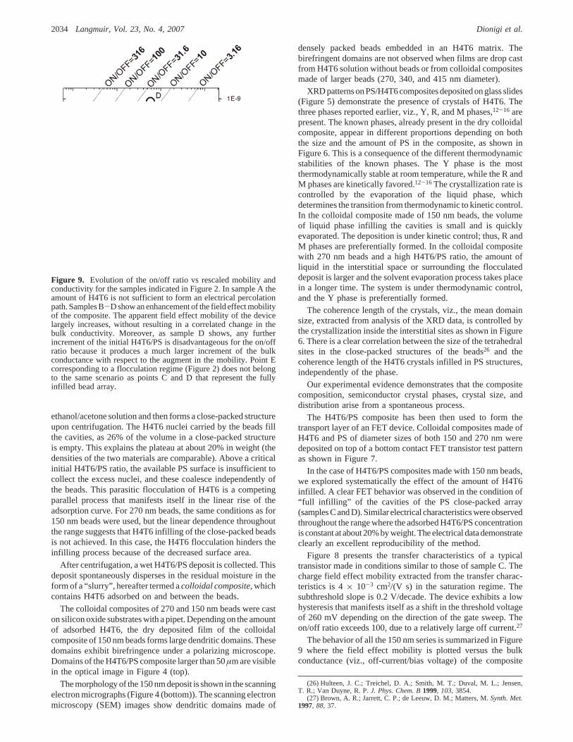
Figure 8 presents the transfer characteristics of a typicaltransistor made in conditions similar to those of sample C. Thecharge field effect mobility extracted from the transfer charac-teristics is 4× 10⁻³ cm2/(V s) in the saturation regime. Thesubthreshold slope is 0.2 V/decade. The device exhibits a lowhysteresis that manifests itself as a shift in the threshold voltageof 260 mV depending on the direction of the gate sweep. Theon/off ratio exceeds 100, due to a relatively large off current.27
The behavior of all the 150 nm series is summarized in Figure9 where the field effect mobility is plotted versus the bulkconductance (viz., off-current/bias voltage) of the composite
(26) Hulteen, J. C.; Treichel, D. A.; Smith, M. T.; Duval, M. L.; Jensen,T. R.; Van Duyne, R. P.J. Phys. Chem. B1999, 103, 3854.
(27) Brown, A. R.; Jarrett, C. P.; de Leeuw, D. M.; Matters, M.Synth. Met.1997, 88, 37.
Figure 9. Evolution of the on/off ratio vs rescaled mobility andconductivity for the samples indicated in Figure 2. In sample A theamount of H4T6 is not sufficient to form an electrical percolationpath. Samples B-D show an enhancement of the field effect mobilityof the composite. The apparent field effect mobility of the devicelargely increases, without resulting in a correlated change in thebulk conductivity. Moreover, as sample D shows, any furtherincrement of the initial H4T6/PS is disadvantageous for the on/offratio because it produces a much larger increment of the bulkconductance with respect to the augment in the mobility. Point Ecorresponding to a flocculation regime (Figure 2) does not belongto the same scenario as points C and D that represent the fullyinfilled bead array.
2034 Langmuir, Vol. 23, No. 4, 2007 Dionigi et al.
material for different H4T6/PS ratios. The transport propertiesare rescaled by the device geometrical parameters.
The transport layer in the FET is formed by the very first fewmonolayers in contact with the dielectric.3,4,28When the amountof H4T6 is below the percolation threshold, no current flows.Consequently, the increment of the initial H4T6/PS (from sampleA to sample C) enhances the on/off ratio by increasing theµ/σratio.27
In Figures 2 and 6 we label as “working transistors” the deviceswhose on/off ratio is in excess of 10. In the case of compositesprepared with 270 nm beads, no FET behavior over the detectionlimit was observed upon an equally systematic analysis.
In this case an incomplete coverage of the device channels ispossibly responsible for the lack of an FET response; viz., theH4T6 crystal domains inside the tetrahedral cavities between thebeads are not connected.
From a morphological point of view (Figure 7), we found thatthe working transistors typically appear largely covered bydendritic domains, whose branches stretch across the channel.From the optical images, a 60-70% coverage of the channel wasestimated. This dendritic morphology does not always determinethe transistors’ operations. FET behavior was found also intransistor channels where no connected dendritic domains were“optically” detected.
We have applied confocal Raman microscopy to FETtransistors to establish a relationship between the crystal structureinside the FET channel and device behavior. Confocal Ramanspectromicroscopy allows us to identify the known crystal phasesof H4T6 and map the spatial distribution of the phase inhomo-
geneity of each sample29 in the transistor channel. The phaseidentification by Raman spectra relies on the different spectralprofiles in the region of the totally symmetric ring vibration.12
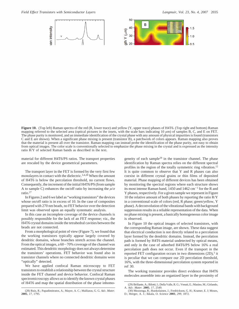
It is quite common to observe that Y and R phases can alsocoexist in different crystal grains or thin films of depositedmaterial. Phase mapping of different devices has been obtainedby monitoring the spectral regions where each structure showsits most intense Raman band, 1450 and 1462 cm-1 for the R andY phases, respectively. For a given sample we represent in Figure10 the relative amount of both phases by reporting the ratio R/Yin a conventional scale of colors (red, R phase; green/yellow, Yphase). A deconvolution of the vibrational bands with backgroundsuppression results in a reliable representation of the data. Whenno phase mixing is present, a basically homogeneous color imageis observed.
In Figure 10 the optical images of selected transistors, withthe corresponding Raman image, are shown. These data suggestthat electrical conduction is not directly related to a percolationlayer formed by the dendritic domains. Instead, the percolationpath is formed by H4T6 material undetected by optical means,and only in the case of adsorbed H4T6/PS below 16% a realpercolation path does not occur. Even if the transport in thereported FET configuration occurs in two dimensions (2D),3 itis peculiar that we can compare our 2D percolation threshold,16%, with the three-dimensional percolation system reported inref 30.
The working transistor provides direct evidence that H4T6molecules assemble into an organized layer in the proximity of
(28) Ruiz, R.; Papadimitratos, A.; Mayer, A. C.; Malliaras, G. G.AdV. Mater.2005, 17, 1795.
(29) Brillante, A.; Bilotti, I.; Della Valle, R. G.; Venuti, E.; Masino, M.; Girlando,A. AdV. Mater. 2005, 17, 2549.
(30) Mezzenga, R.; Ruokolainen, J.; Fredrickson, G. H.; Kramer, E. J; Moses,D.; Heeger, A. J.; Ikkala, O.Science2003, 299, 1872.
Figure 10. (Top left) Raman spectra of the red (R, lower trace) and yellow (Y, upper trace) phases of H4T6. (Top right and bottom) Ramanmapping referred to the selected area (optical pictures in the insets, with the scale bars indicating 10µm) of samples B, C, and E on FET.The phase purity is monitored, and an immediate identification of the crystal phase with any amount of physical impurities is found (transistorsC and E are shown). When a significant phase mixing is present (transistor B), a patchwork of colors appears. Raman mapping also provesthat the material is present all over the transistor. Raman mapping can instead probe the identification of the phase purity, not easy to obtainfrom optical images. The color scale is conventionally selected to emphasize the phase mixing in the crystal and is expressed as the intensityratio R/Y of selected Raman bands as described in the text.
Field Effect Transistors with Semiconductor Layers Langmuir, Vol. 23, No. 4, 20072035
the dielectric surface. This strongly supports a scenario wherethe H4T6 aggregates carried by the beads crystallize insidetemplate channels owing to the slower solvent evaporation. Thevariability of domain formation with respect to the bead diametercan be ascribed to the two scales of the process: (a) asubmicrometer scale which is imposed by the templating beads;(b) a nanometer scale characteristic of diffusion/aggregation/crystallization of H4T6 molecules and clusters. The latter processshould not be critically influenced by the mesoscopic self-assembly of the templating beads as long as their characteristicsize does not restrict flow or diffusion of H4T6. However, thesize of the empty space among the beads (tetrahedral cavities)critically influences the time of the solvent evaporation dis-criminating both phase content and crystal size.
Raman spectroscopy shows that the morphological andcompositional characteristic of the dry PS/H4T6 composite inthe FET channel is in agreement with a dominant concentrationof R and M phases as detected by XRD of composites on a glasssubstrate. The strength ofπ-stacking decreases in the order R> M > Y as confirmed by the trend of the intermoleculardistances.12-16 The orientation of the active molecules in theFET channel5,6,31is the factor affecting the charge mobility. Evenif we do not have direct evidence of the molecular orientationin proximity of the substrate in the FET channel, the orientationsof both R and M phases in the bulk PS/H4T6 are the same asthose observed in thin films of H4T6 obtained by high-vacuumevaporation onto dielectric substrates using different depositionrates and substrate temperatures.16,32
In all the bulk phases the assumed orientations are the mostsuitable for large charge mobility (Figure 5) with the molecules
standing up onto the substrate and facing each other to maximizeπ-stacking.12-16,32
As a comparison, thin film transistors by spin-casting of H4T6solutions exhibit mobilities of 10-5 cm2/(V s). It has to be saidthat, in the case of these solutions, the wetting of the substrateis a problem, since H4T6 wets preferentially the gold pads andit is very difficult to cast a continuous film between the drainand source. As a result spin casting on the test pattern yields apercolation path not sufficiently connected.
Conclusions
We have demonstrated the possibility to induce H4T6molecular ordering on an FET by controlling the crystallizationof an organic semiconductor within a template made of self-assembled dielectric beads. The crystals of all the phases formedwithin the tetrahedral interbead cavities are oriented with respectto the S/D electrodes along directions allowing charge transport.It is important to underline that the conjugated homologuesexithienyl grown as a highly ordered26,33thin film on a devicestructure3 by ultra-high-vacuum sublimation in an OMBDapparatus exhibits on the same test patterns a charge mobilityon the order of 0.01-0.05 cm2/(V s). Our dispersion-casttransistors with 150 nm beads exhibit a charge mobility that is2-10 times smaller. The method we have proposed for depositingthe active layer from bead carriers is completely general forsoluble semiconductors. The complete use of water-basedsolutions offers the interesting opportunity of fabricating organicelectronic devices by a “chimie douce” approach.
Acknowledgment. This work was supported by the EUIntegrated Project NAIMO (Grant NMP4-CT-2004-500355). Wethank Dr. Maria Antonietta Loi for help with the confocal laserscanning microscopy. P.S. acknowledges support of the ICTPProgramme for Training and Research in Italian Laboratories,Trieste, Italy.
LA062371K
(31) DeLongchamp, D. M.; Jung, Y.; Fischer, D. A.; Lin, E. K.; Chang, P.;Subramanian, V.; Murphy, A. R.; Fre´chet, J. M. J.J. Phys. Chem. B2006, 110,10645.
(32) Porzio, W.; Giovanella, U.; Pasini, M.; Botta, C.; Destri, S.; Provasi, C.Thin Solid Films2004, 466, 231.
(33) Dinelli, F.; Moulin, J. F.; Loi, M. A.; Da Como, E.; Massi, M.; Murgia,M.; Muccini, M.; Biscarini, F.; Wie, J.; Kingshott, P.J. Phys. Chem. B2006, 110,258.
2036 Langmuir, Vol. 23, No. 4, 2007 Dionigi et al.