
Diapositive del corso: Circuiti Elettronici di Potenza L · Sviluppo dell’elettronica di potenza...
160
Corso di Laurea in Ingegneria Elettrica A.A. 2007/2008 Diapositive del corso: Circuiti Elettronici di Potenza L Docente: prof. Gabriele Grandi
Transcript of Diapositive del corso: Circuiti Elettronici di Potenza L · Sviluppo dell’elettronica di potenza...
Corso di Laurea in Ingegneria Elettrica
A.A. 2007/2008
Diapositive del corso: Circuiti Elettronici di Potenza L
Docente: prof. Gabriele Grandi

Circuiti Elettronici di Potenza
Docente: prof. Gabriele GRANDIDipartimento di Ingegneria Elettrica
http://www.die.ing.unibo.it/cep.htm
E-mail: [email protected]. 051-20-93571Fax. 051-20-93588
PromemoriaLista e-mail studenti CEP-2009 , pw: 2009Propedeuticità (http://www.dsa.unibo.it)Corsi a valle III anno e LM (novità!)Modalità d’esameDate degli appelli d’esameRicognizione problematiche StudentiPresentazione del Corso
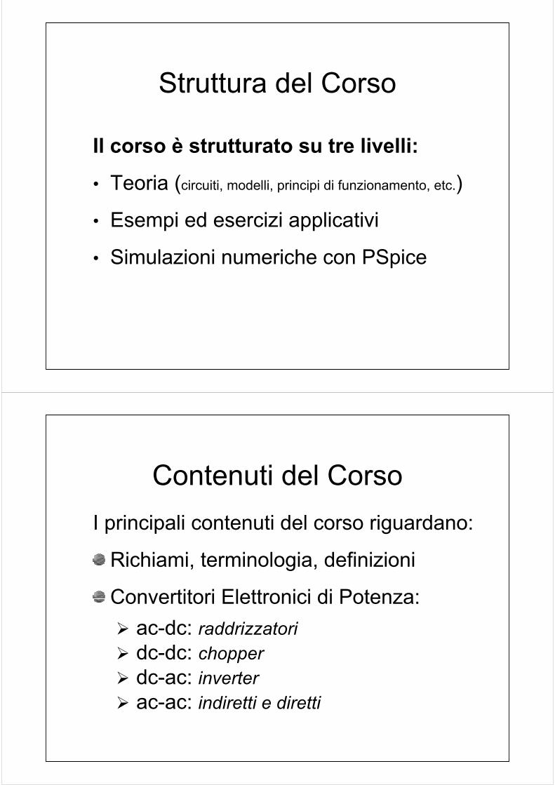
Struttura del Corso
Il corso è strutturato su tre livelli:
• Teoria (circuiti, modelli, principi di funzionamento, etc.)
• Esempi ed esercizi applicativi
• Simulazioni numeriche con PSpice
Contenuti del CorsoI principali contenuti del corso riguardano:
Richiami, terminologia, definizioni
Convertitori Elettronici di Potenza:ac-dc: raddrizzatoridc-dc: chopperdc-ac: inverterac-ac: indiretti e diretti
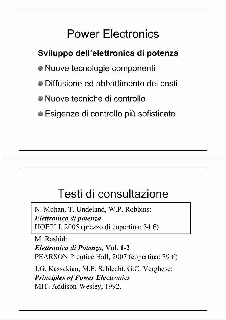
Power ElectronicsSviluppo dell’elettronica di potenza
Nuove tecnologie componenti
Diffusione ed abbattimento dei costi
Nuove tecniche di controllo
Esigenze di controllo più sofisticate
Testi di consultazioneN. Mohan, T. Undeland, W.P. Robbins:Elettronica di potenzaHOEPLI, 2005 (prezzo di copertina: 34 €)M. Rashid:Elettronica di Potenza, Vol. 1-2PEARSON Prentice Hall, 2007 (copertina: 39 €)J.G. Kassakian, M.F. Schlecht, G.C. Verghese:Principles of Power ElectronicsMIT, Addison-Wesley, 1992.
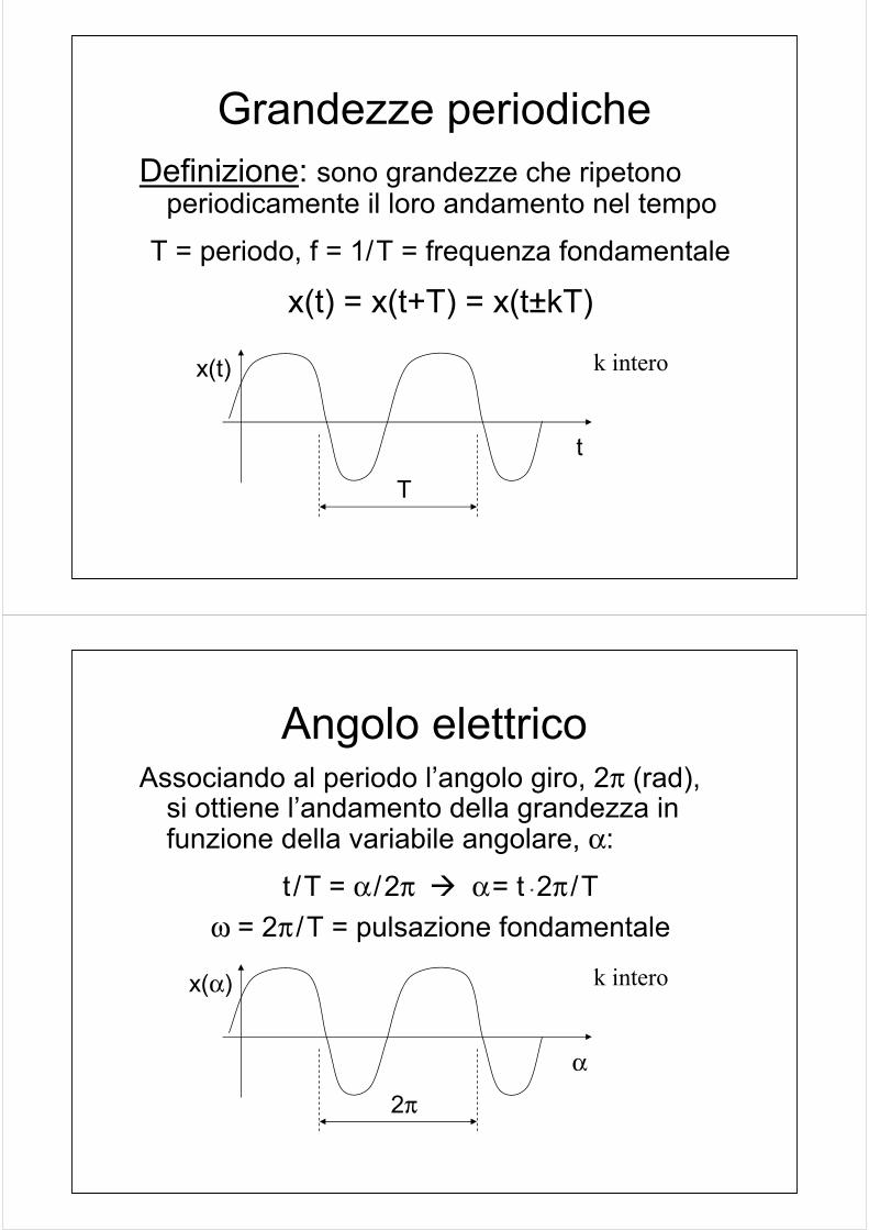
Grandezze periodicheDefinizione: sono grandezze che ripetono
periodicamente il loro andamento nel tempo
T = periodo, f = 1/T = frequenza fondamentale
x(t) = x(t+T) = x(t±kT)
T
t
x(t) k intero
Angolo elettricoAssociando al periodo l’angolo giro, 2π (rad),
si ottiene l’andamento della grandezza in funzione della variabile angolare, α:
t /T = α /2π α= t * 2π /Tω = 2π /T = pulsazione fondamentale
2π
α
x(α) k intero

Valore medio - Definizione
T
t
x(t) Xm
∫+
==Tt
t
m
o
o
dt)t(xT
)T(xX 1to arbitrario
Valore medio - GraficaGraficamente è rappresentato dalla ordinata di
bilanciamento delle aree
area (+) = area (-)
T
t
x(t) Xm
0])([1 =−∫+Tt
t
m
o
o
dtXtxT
Valore medio - Proprietà (1)
Per grandezze isofrequenziali (periodo T) si ha:
(T)y(T)x(T)yx +=+
(T)xk(T)xk =
(T)yk(T)xk(T)ykxk 2121 +=+
Valore medio combinazione lineare = comb. lineare dei valori medi
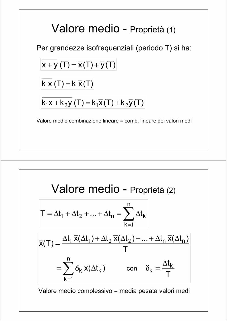
Valore medio - Proprietà (2)
Valore medio complessivo = media pesata valori medi
∑=
∆=∆++∆+∆=n
kkn tt...ttT
121
Tt )t(x
T)t(xt...)t(xt)t(xt)T(x
kk
n
kkk
nn
con∆=δ∆δ=
∆∆++∆∆+∆∆=
∑=1
2211

Valore efficace - Definizione
∫+
===Tt
t
eff
o
o
dt)t(xT
)T(x~XX 21to arbitrario
Radice quadrata della media dei quadrati nel periodo
Definizione analoga utilizzando la variabile angolare α(t)
Valore efficace - Grafica
T
t
x(t)
X2eff
x2(t)
0])([1 22 =−∫+Tt
t
o
o
eff dtXtxT

Valore efficace - Proprietà
Radice della media pesata dei quadrati
∑=
∆=∆++∆+∆=n
kkn tt...ttT
121
Tt )t(x~)T(x~
T)t(x~t...)t(x~t)t(x~t)T(x~
kk
n
kkk
nn
con∆=δ∆δ=
∆∆++∆∆+∆∆=
∑=1
2
22
221
212
Sviluppo in serie di Fourier (1)
Una qualsiasi grandezza periodica può essere scomposta in una somma di sinusoidi con frequenza multipla della fondamentale
∑∑∞
=
∞
=
ω+ω+=11 k
kk
ko )tk(senb)tkcos(aa)t(x
ao = Xm = Xo = valor medio
ω = 2π /T = 2π f = pulsazione fondamentale
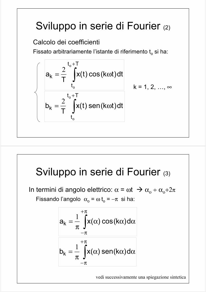
Sviluppo in serie di Fourier (2)
∫+
ω=Tt
tk
o
o
dt)tk(cos)t(xT
a 2
Calcolo dei coefficienti
∫+
ω=Tt
tk
o
o
dt)tk(sen)t(xT
b 2
Fissato arbitrariamente l’istante di riferimento to si ha:
k = 1, 2, …, ∞
Sviluppo in serie di Fourier (3)
∫π+
π−
αααπ
= d)k(cos)(xak1
In termini di angolo elettrico: α = ωt αο ÷ αο+2π
∫π+
π−
αααπ
= d)k(sen)(xbk1
Fissando l’angolo αo = ω to = −π si ha:
vedi successivamente una spiegazione sintetica

Sviluppo in serie di Fourier (4)
22kkk bac +=
Espressione compatta
=ϕ
k
kk a
btgarc
∑∞
=
ϕ−ω+=1k
kko )tkcos(cX)t(x
ak
bk
ck
( ) ( ) ( ) ( ) ( ) ( )[ ]( ) ( ) ... s cb , ca
stkstkctksbtka
kkkkkk
kkkkk
one...Dimostrazi
⇒ϕ=ϕ=ϕω+ϕω=ω+ω
incosinincoscosincos
ϕk
444 3444 21 )( kk tkcosc ϕ−ω
Sviluppo in serie di Fourier (5)
)tkcos(X)t(x kkk ϕ−ω= 2
∑∞
=
+=1k
ko )t(xX)t(x
xk(t) è l’armonica k- esima di x(t)
frequenza: k f , valore efficace:2k
kcX =
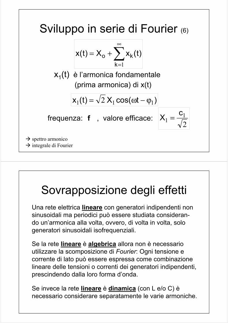
Sviluppo in serie di Fourier (6)
)tcos(X)t(x 111 2 ϕ−ω=
∑∞
=
+=1k
ko )t(xX)t(x
x1(t) è l’armonica fondamentale(prima armonica) di x(t)
frequenza: f , valore efficace:21
1cX =
spettro armonicointegrale di Fourier
Sovrapposizione degli effettiUna rete elettrica lineare con generatori indipendenti non sinusoidali ma periodici può essere studiata consideran-do un’armonica alla volta, ovvero, di volta in volta, solo generatori sinusoidali isofrequenziali.
Se la rete lineare è algebrica allora non è necessario utilizzare la scomposizione di Fourier: Ogni tensione e corrente di lato può essere espressa come combinazione lineare delle tensioni o correnti dei generatori indipendenti,prescindendo dalla loro forma d’onda.
Se invece la rete lineare è dinamica (con L e/o C) ènecessario considerare separatamente le varie armoniche.
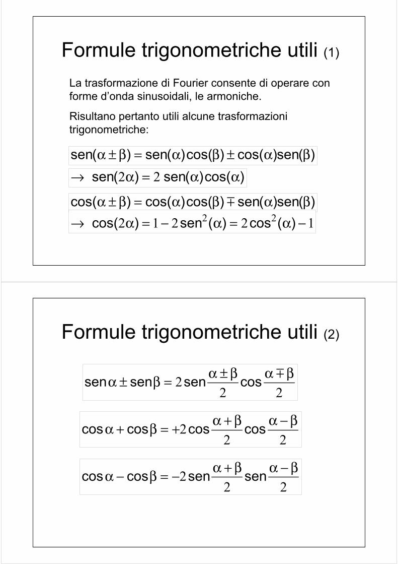
Formule trigonometriche utili (1)
)(sen)cos()cos()(sen)(sen βα±βα=β±α
Risultano pertanto utili alcune trasformazioni trigonometriche:
La trasformazione di Fourier consente di operare con forme d’onda sinusoidali, le armoniche.
)(sen)(sen)cos()cos()cos( βαβα=β±α m
)cos()(sen)(sen αα=α→ 22
12212 22 −α=α−=α→ )(cos)(sen)cos(
Formule trigonometriche utili (2)
222 βαβ±α=β±α mcossensensen
222 β−αβ+α+=β+α coscoscoscos
222 β−αβ+α−=β−α sensencoscos
Formule trigonometriche utili (3)
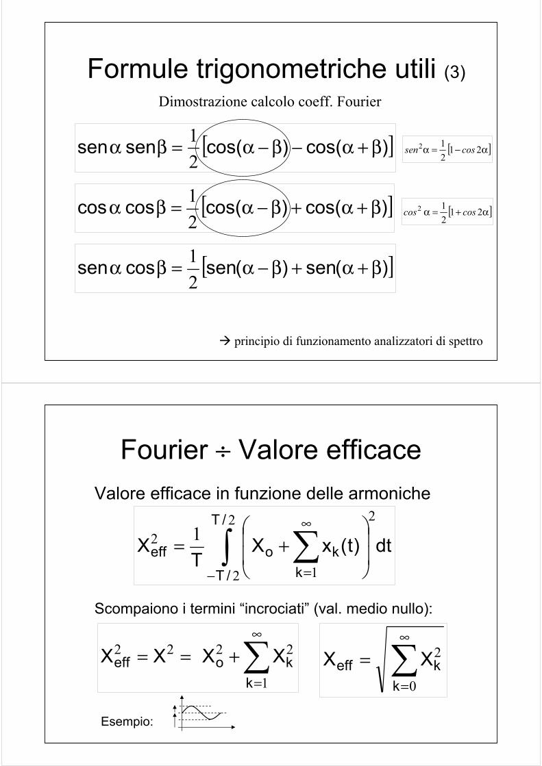
[ ])cos()cos(sensen β+α−β−α=βα21
[ ])cos()cos(coscos β+α+β−α=βα21
[ ])(sen)(sencossen β+α+β−α=βα21
Dimostrazione calcolo coeff. Fourier
principio di funzionamento analizzatori di spettro
[ ]α−=α 21212 cossen
[ ]α+=α 21212 coscos
Fourier ÷ Valore efficaceValore efficace in funzione delle armoniche
∑∞
=
=0
2
kkeff XX∑
∞
=
+==1
2222
kkoeff XXXX
dt)t(xXT
X/T
/T kkoeff ∫ ∑
−
∞
=
+=
2
2
2
1
2 1
Scompaiono i termini “incrociati” (val. medio nullo):
Esempio:

Alcuni casi particolari: pari
Il calcolo dei coeff. della serie di Fourier risulta sempli-ficato nel caso la forma d’onda presenti simmetrie:
funzione “pari”:
x(α) = x(-α)
Simmetria rispetto l’asse x = 0
∫π
αααπ
=
o
k d)k(cos)(xa 2
0=kb scompaiono i terminiin “seno”
pari
Esempio: funzione pari
α = ωt
2π
x(α) = x(-α)
( α ) (−α ) :
x(-α) cos(-kα) = x(α) cos(kα)
x(-α) sen(-kα) = − x(α) sen(kα)
Alcuni casi particolari: dispari
funzione “dispari”:
x(α) = − x(-α)
Anti-simmetria rispetto l’asse x = 0
0=ka scompaiono i terminiin “coseno”
∫π
αααπ
=
o
k d)k(sen)(xb 2
dispari
Esempio: funzione dispari
α = ωt
2π
x(α) = − x(-α)( α ) (−α ) :
x(-α) cos(-kα) = − x(α) cos(kα)
x(-α) sen(-kα) = x(α) sen(kα)

Alcuni casi particolari: semi-onda
x(α) = − x(α±π)Semionde (+) e (−) identiche e traslate:
∫π
αααπ
=0
2 d)k(sen)(xbk
∫π
αααπ
=0
2 d)k(cos)(xak
coeff. ≠≠≠≠ 0 solo per k dispari:coeff. = 0 per k pari:
0=ka
0=kb
Esempio: semi-onda
α = ωt
2π
x(α) = − x(α±π)( α ) (α+π ) :
x(α+ π) = − x(α)
x(α+π) cos[k(α+π)] = − x(α) cos(kα+kπ) k pari − x(α) cos(kα)k dispari x(α) cos(kα)
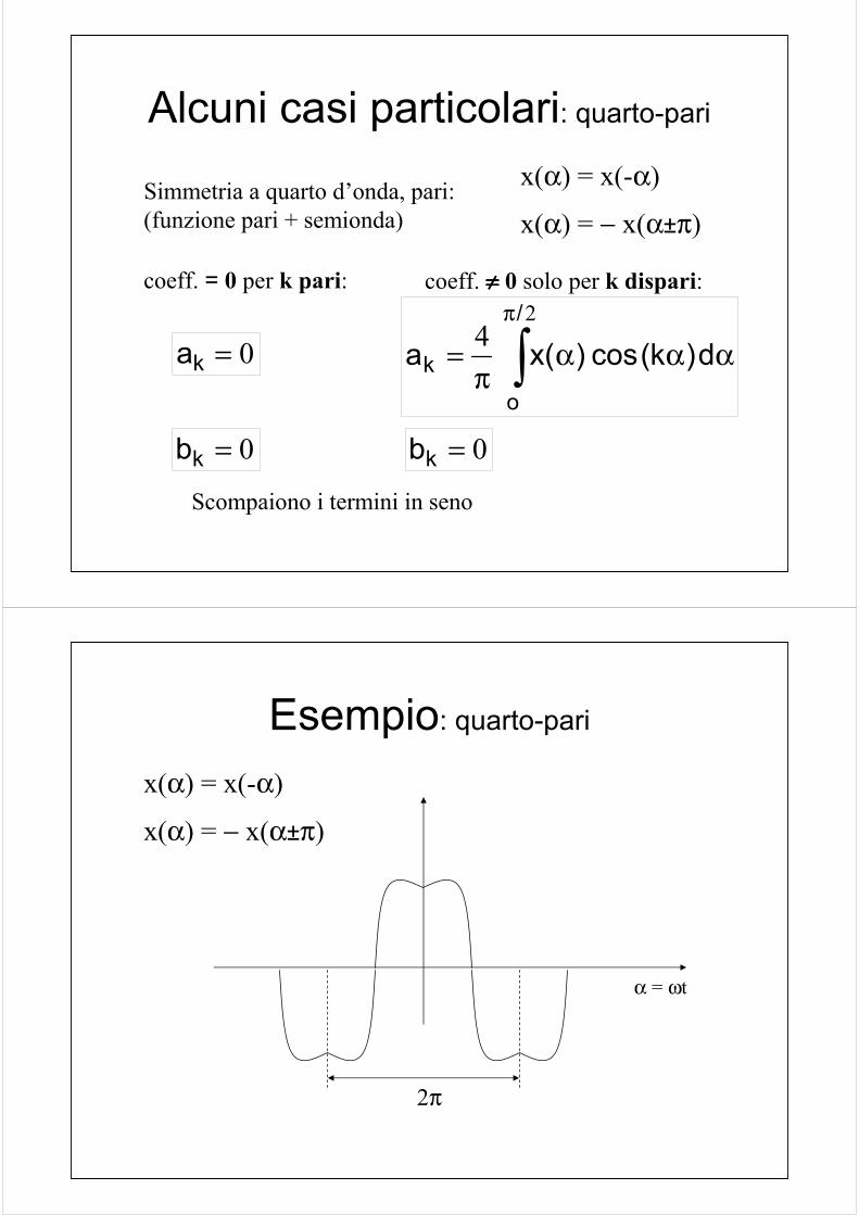
Alcuni casi particolari: quarto-pari
x(α) = − x(α±π)Simmetria a quarto d’onda, pari:(funzione pari + semionda)
0=kb
∫π
αααπ
=2
4/
o
k d)k(cos)(xa
coeff. ≠≠≠≠ 0 solo per k dispari:coeff. = 0 per k pari:
0=ka
0=kb
x(α) = x(-α)
Scompaiono i termini in seno
Esempio: quarto-pari
x(α) = − x(α±π)
x(α) = x(-α)
2π
α = ωt
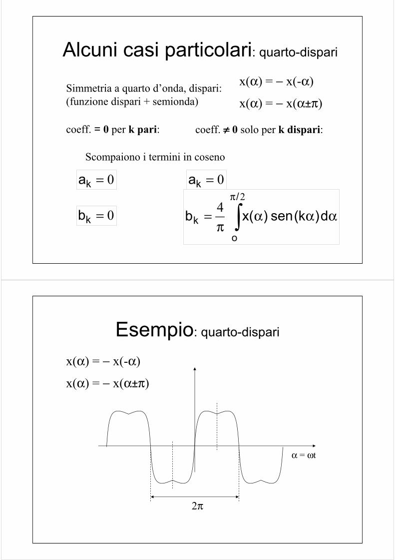
Alcuni casi particolari: quarto-dispari
x(α) = − x(α±π)Simmetria a quarto d’onda, dispari:(funzione dispari + semionda)
coeff. ≠≠≠≠ 0 solo per k dispari:coeff. = 0 per k pari:
0=ka
0=kb
x(α) = − x(-α)
∫π
αααπ
=2
4/
o
k d)k(sen)(xb
0=ka
Scompaiono i termini in coseno
Esempio: quarto-dispari
x(α) = − x(α±π)
x(α) = − x(-α)
2π
α = ωt

Distorsione armonicaConsideriamo ora grandezze alternate (X0= 0).Rispetto alla fondamentale (prima armonica) le armoniche di ordine superiore costituiscono un contributo di distorsione.
∑∞
=
+=2
1k
k )t(x)t(x)t(x
∑∞
=
=−=2
1k
kdist )t(x)t(x)t(x)t(x
Distorsione armonica÷ Val.eff.In termini di valore efficace, la distorsione armonica risulta:
∑∞
=
=−=2
221
22
kkeffdist XXXX
∑∞
=
=2
2
kkdist XXdttx
TX
/T
/T kkdist ∫ ∑
−
∞
=
=
2
2
2
2
2 )(1
dttxtxT
X/T
/T kkeff ∫ ∑
−
∞
=
+=
2
2
2
21
2 )()(1

Distorsione armonica÷ THD (1)
Si definisce il fattore di distorsione armonica totale:
THD = Total Harmonic Distortion
1001
⋅=X
X(%)THD dist
Rappresenta la distorsione armonica rapportata all’armonica fondamentale
Distorsione armonica÷ THD (2)
Il THD può essere espresso anche con le formulazioni:
1002
2
1⋅
= ∑
∞
=k
kXX(%)THD
10012
1⋅−
=
XX(%)THD eff
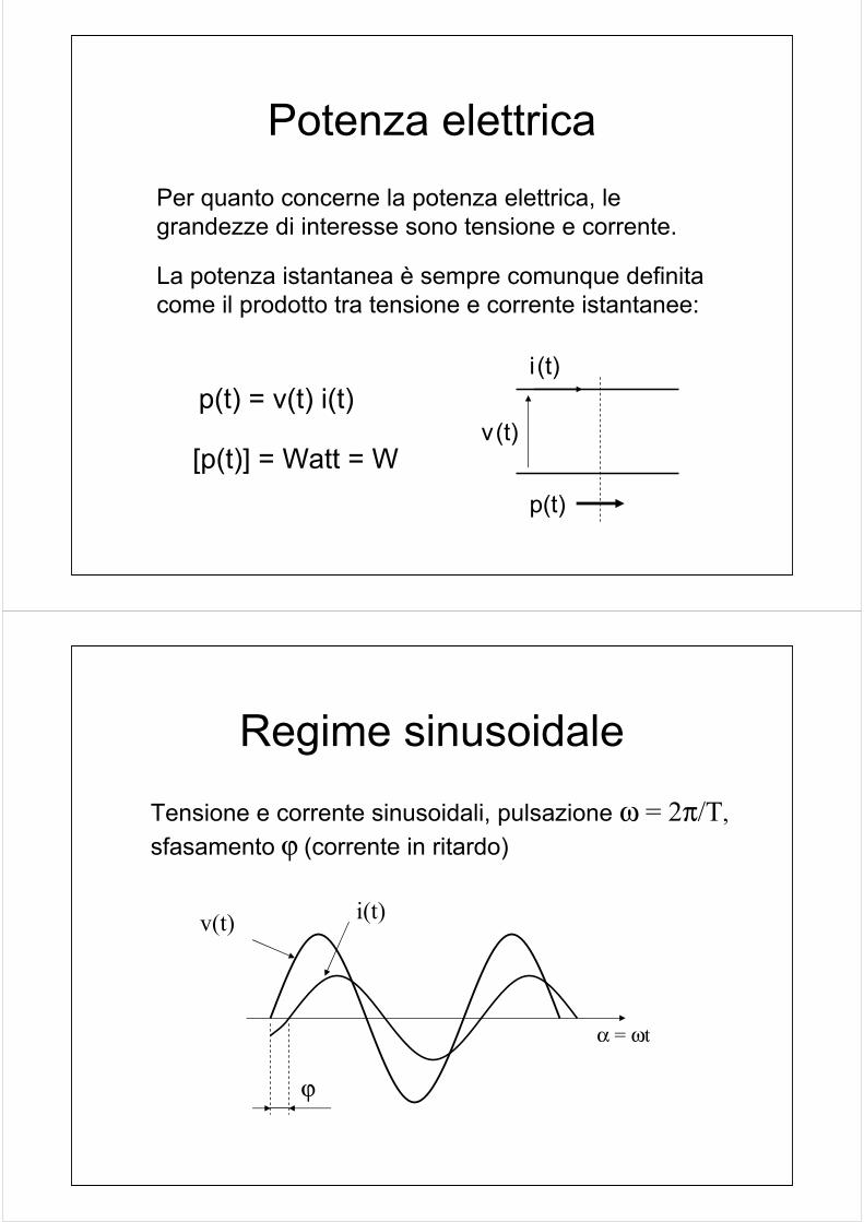
Potenza elettricaPer quanto concerne la potenza elettrica, le grandezze di interesse sono tensione e corrente.
La potenza istantanea è sempre comunque definitacome il prodotto tra tensione e corrente istantanee:
p(t) = v(t) i(t)
[p(t)] = Watt = Wv(t)
i(t)
p(t)
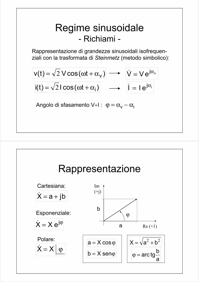
Regime sinusoidale
Tensione e corrente sinusoidali, pulsazione ω = 2π/T, sfasamento ϕ (corrente in ritardo)
α = ωt
ϕ
v(t) i(t)
Regime sinusoidale- Richiami -
Rappresentazione di grandezze sinusoidali isofrequen-ziali con la trasformata di Steinmetz (metodo simbolico):
)t(cosV)t(v vα+ω= 2
)t(cosI)t(i iα+ω= 2
vjeVV α=&
ijeII α=&
Angolo di sfasamento V÷I : ϕ = αv − αi
Rappresentazione
ϕ= jeXX& Re (+1)
Im(+j) X&bjaX +=&
Cartesiana:
Esponenziale: ϕ
Polare:
ϕ= XX&
b
a
ϕ= cosXa
ϕ= senXb
22 baX +=
abtgarc=ϕ
Potenza in regime sinusoidale
In regime sinusoidale, con riferimento al periodo T,si definisce la potenza media potenza attiva
∫∫++
===Tt
t
Tt
t
o
o
o
o
dt)t(i)t(vT
dt)t(pT
)T(pP 11
ϕ== cosIV)T(pP
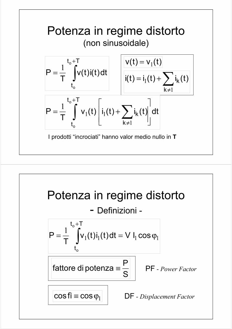
Regime non sinusoidale
α = ωt
ϕ1
v(t) = v1(t)
i(t)
i1(t)
Spesso accade che la tensione sia praticamente sinusoidalementre la corrente si presenta fortemente distorta:
Potenza in regime distorto(non sinusoidale)
∫+
=Tt
t
o
o
dt)t(i)t(vT
P 1
∫ ∑+
≠
+=
Tt
t kk
o
o
dt)t(i)t(i)t(vT
P1
111
)t(v)t(v 1=
∑≠
+=1
1k
k )t(i)t(i)t(i
I prodotti “incrociati” hanno valor medio nullo in T
Potenza in regime distorto- Definizioni -
11111 ϕ== ∫
+
cosIVdt)t(i)t(vT
PTt
t
o
o
SPpotenza di fattore ≡
1ϕ≡ cosfìcos
PF - Power Factor
DF - Displacement Factor
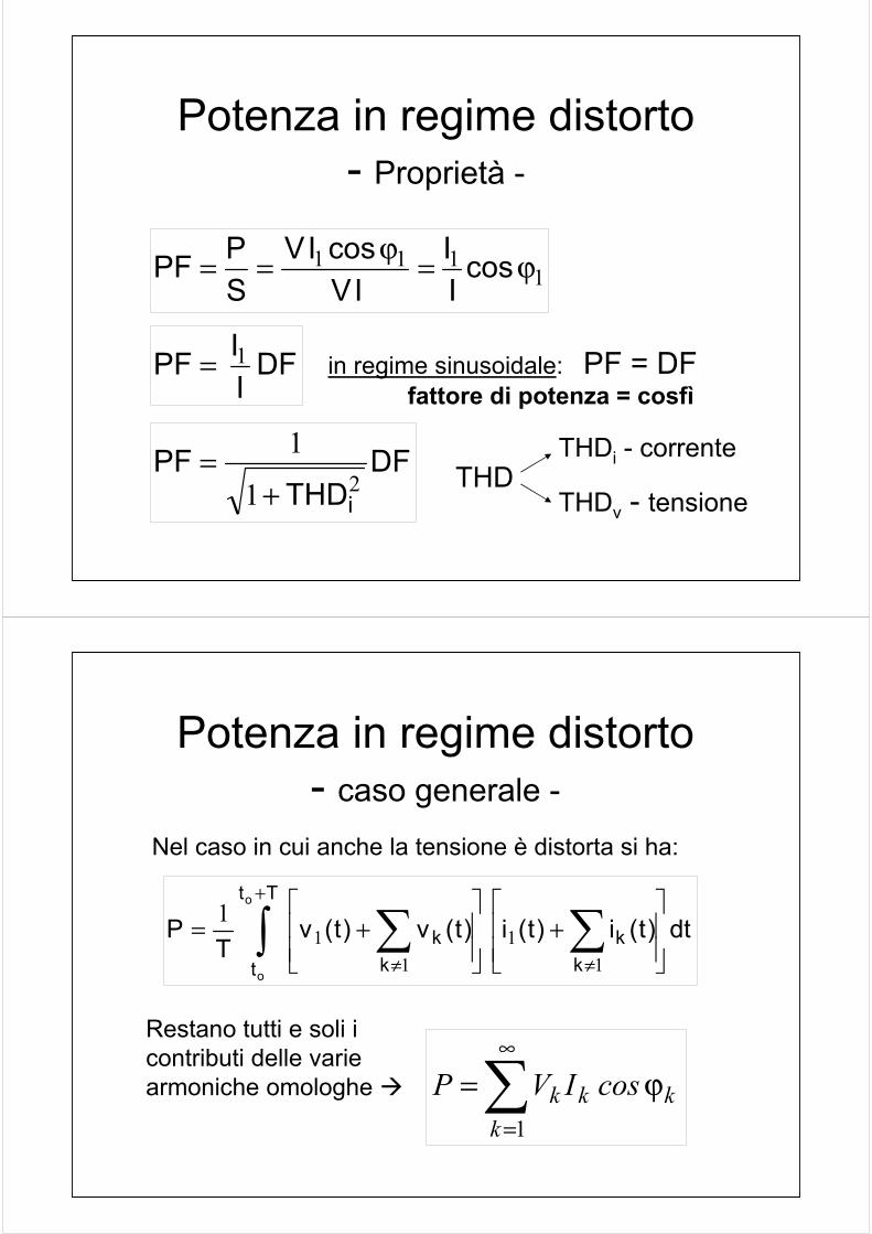
Potenza in regime distorto- Proprietà -
in regime sinusoidale: PF = DFfattore di potenza = cosfì
1111 ϕ=ϕ== cosII
IVcosIV
SPPF
DFIIPF 1=
DFTHD
PFi21
1
+= THD
THDi - corrente
THDv - tensione
Nel caso in cui anche la tensione è distorta si ha:
Potenza in regime distorto- caso generale -
∫ ∑∑+
≠≠
+
+=
Tt
t kk
kk
o
o
dt)t(i)t(i)t(v)t(vT
P1
11
11
∑∞
=
ϕ=1k
kkk cosIVP
Restano tutti e soli i contributi delle varie armoniche omologhe
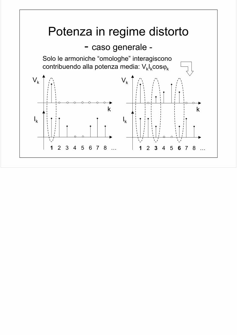
Solo le armoniche “omologhe” interagisconocontribuendo alla potenza media: VkIkcosϕk
Potenza in regime distorto- caso generale -
Vk
Ik
k
1 2 3 4 5 6 7 8 …
Vk
Ik
k
1 2 3 4 5 6 7 8 …
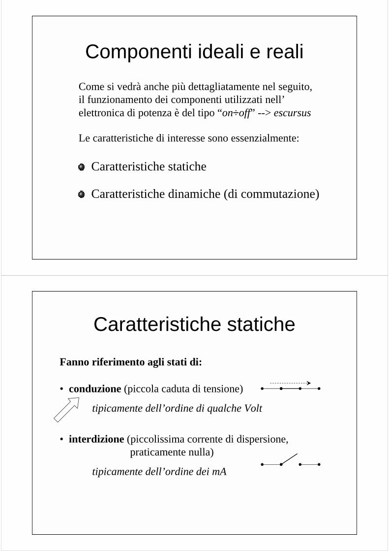
Componenti ideali e reali
Le caratteristiche di interesse sono essenzialmente:
Caratteristiche statiche
Caratteristiche dinamiche (di commutazione)
Come si vedrà anche più dettagliatamente nel seguito,il funzionamento dei componenti utilizzati nell’elettronica di potenza è del tipo “on÷off” --> escursus
Caratteristiche statiche
Fanno riferimento agli stati di:
• conduzione (piccola caduta di tensione)
tipicamente dell’ordine di qualche Volt
• interdizione (piccolissima corrente di dispersione, praticamente nulla)
tipicamente dell’ordine dei mA
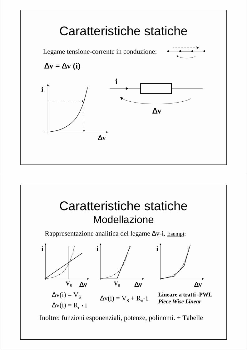
Caratteristiche statiche
∆∆∆∆v
i
Legame tensione-corrente in conduzione:
∆∆∆∆v = ∆∆∆∆v (i)
i
∆∆∆∆v
Caratteristiche staticheModellazione
Rappresentazione analitica del legame ∆v-i. Esempi:
Lineare a tratti -PWLPiece Wise Linear
∆∆∆∆v
ii
VS
∆v(i) = VS + Ro• i
∆∆∆∆v
Inoltre: funzioni esponenziali, potenze, polinomi. + Tabelle
i
VS ∆∆∆∆v∆v(i) = VS
∆v(i) = Rc • i

Caratteristiche dinamiche
Fanno riferimento alle commutazioni on÷÷÷÷off:(tipicamente dell’ordine dei µµµµs)
• accensione (turn-on)
tempo di accensione = ton = td-on + tr
= tempo di ritardo + tempo si salita
• spegnimento (turn-off)
tempo di spegnimento = toff = td-off + tf
= tempo di ritardo + tempo si discesa
Caratteristiche dinamiche Definizioni
x(t)
Xreg
10% Xreg
90% Xreg
vc(t)
td-on tr td-off tf
salita (rise)
discesa (fall)controllo
tritardo (delay)
ton toff
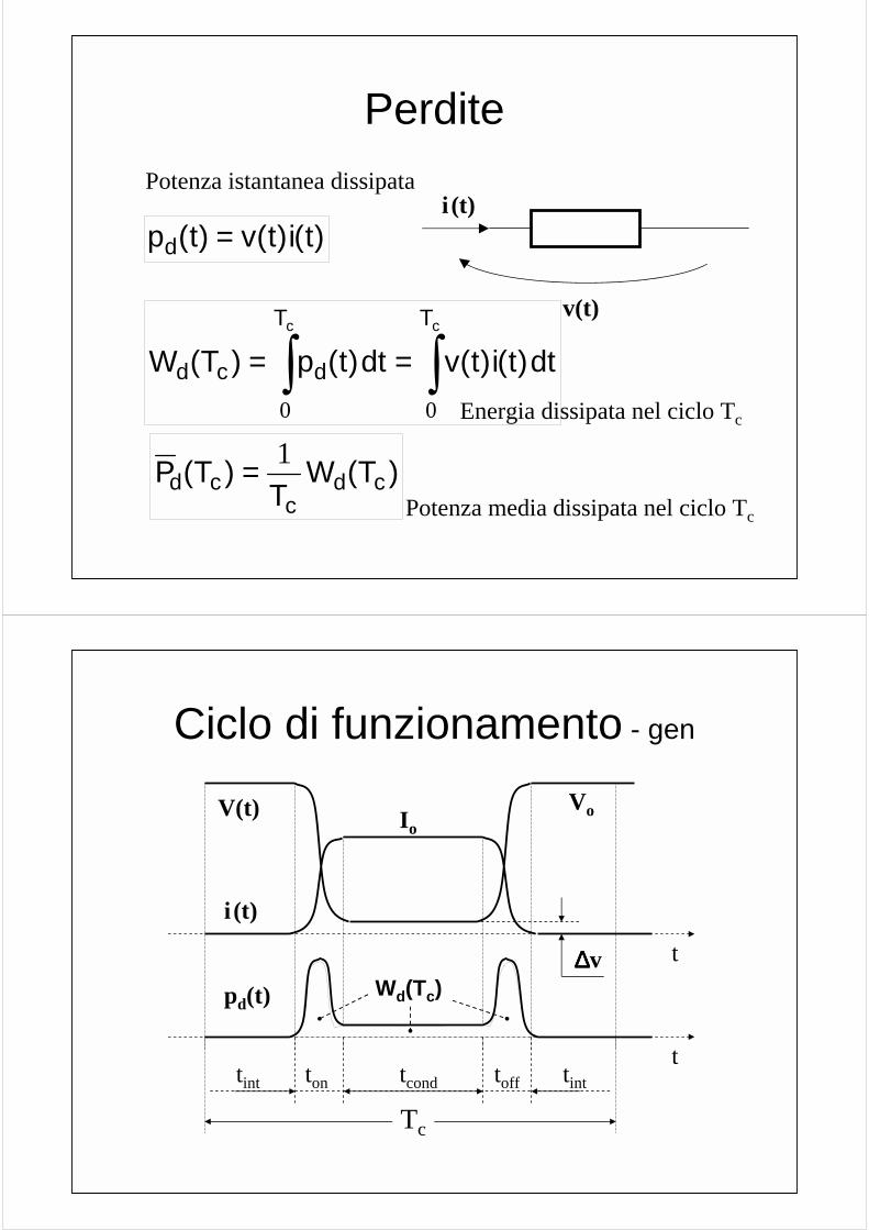
Perdite
v(t)
i (t)
∫∫ ==cc TT
dcd dt)t(i)t(vdt)t(p)T(W00
)t(i)t(v)t(pd =
Potenza istantanea dissipata
)T(WT
)T(P cdc
cd1=
Potenza media dissipata nel ciclo Tc
Energia dissipata nel ciclo Tc
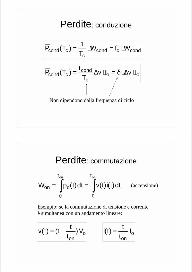
Ciclo di funzionamento - gen
V(t)
i (t)
tint tintton tofftcond
Tc
∆∆∆∆v
IoVo
Wd(Tc)pd(t)
t
t

Perdite: conduzione
∫∫ ==condcond tt
dcond dt)t(i)t(vdt)t(pW00
Le perdite in interdizione sono praticamente nulle (i ≅≅≅≅ 0)
Le perdite di conduzione sono:
tcond >> ton , toff tcond = δ Tc
duty-cycletcond + tint ≅ Tc
Perdite: conduzione
∆∆∆∆v
ipunto di lavoro
Area = perdite di conduzione
condo
t
o
t
dcond tIvdtIvdt)t(pWcondcond
⋅⋅∆=⋅∆== ∫∫00
Io
v
Io ≅ cost. in tcond
Perdite: conduzione
ooc
condccond IvIv
Tt)T(P ⋅∆⋅δ=⋅∆=
condccondc
ccond WfWT
)T(P ⋅=⋅= 1
Non dipendono dalla frequenza di ciclo
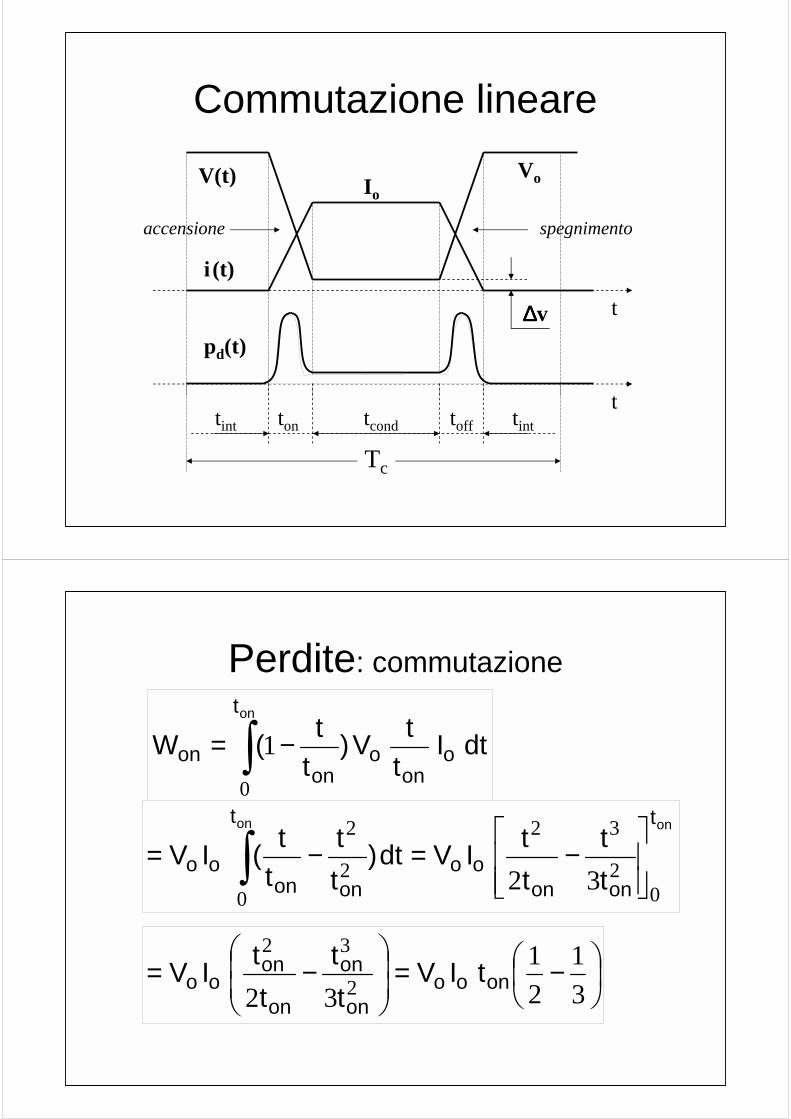
Perdite: commutazione
∫∫ ==onon tt
don dt)t(i)t(vdt)t(pW00
oon
V)tt()t(v −= 1 o
onI
tt)t(i =
Esempio: se la commutazione di tensione e corrente è simultanea con un andamento lineare:
(accensione)
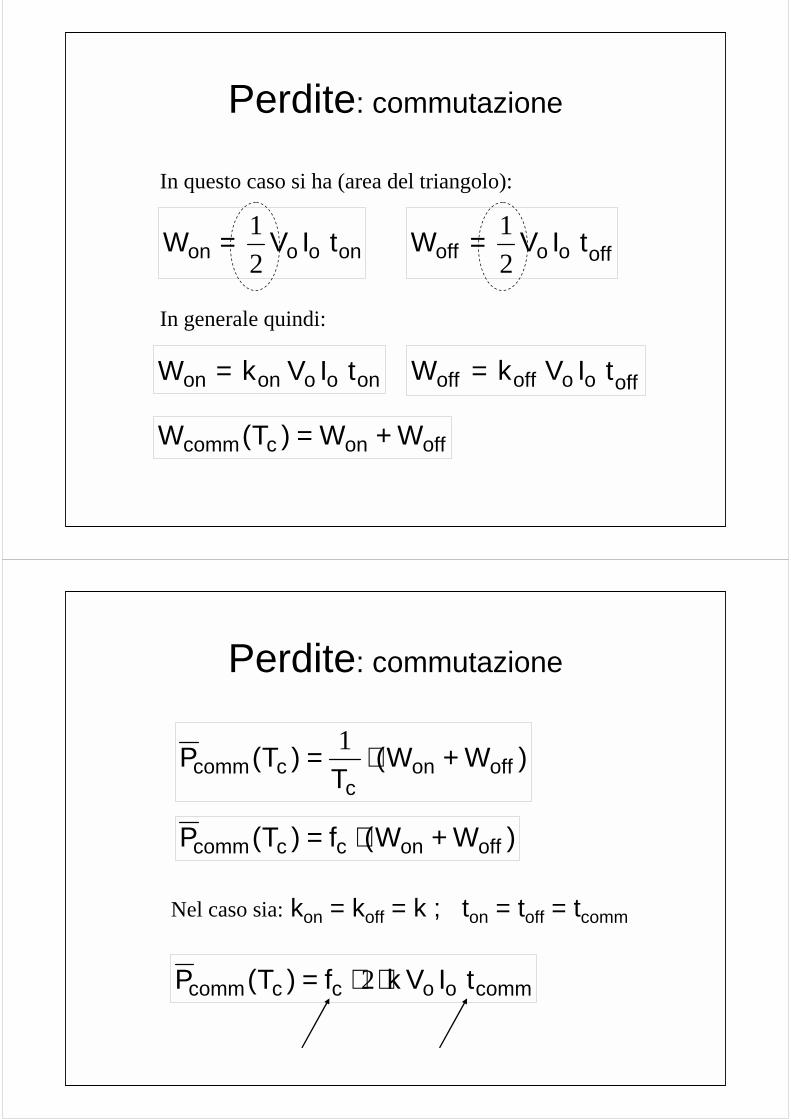
Commutazione lineare
V(t)
tint tintton tofftcond
Tc
∆∆∆∆v
i(t)
IoVo
pd(t)
t
t
accensione spegnimento
Perdite: commutazione
∫ −=ont
oon
oon
on dtIttV)
tt(W
0
1
onon t
ononoo
t
ononoo t
tttIVdt)
tt
tt(IV
02
32
02
2
32
−=−= ∫
−=
−=
31
21
32 2
32
onooon
on
on
onoo tIV
tt
ttIV

Perdite: commutazione
onooon tIVW ⋅⋅=61
21
61 ÷=k
L’andamento effettivo di v(t) ed i(t)porta a valori di k superiori:
offonoooffon tIVkW ÷÷ ⋅⋅=
Nella realtà spesso la commutazione di tensione e corrente non avviene simultaneamente, con una conseguente maggiore dissipazione.
Supponendo la commutazione sia lineare, ma non simultanea:
analogamente perlo spegnimento:
Ciclo di funzionamento - rit
V(t)
pd(t)
ton toff
∆∆∆∆v
i(t)
IoVo
t
ttri tfv trv tfi
Perdite: commutazione
onooon tIVW21=
onooonon tIVkW = offoooffoff tIVkW =
offonccomm WW)T(W +=
In questo caso si ha (area del triangolo):
offoooff tIVW21=
In generale quindi:
Perdite: commutazione
)WW(T
)T(P offonc
ccomm +⋅= 1
)WW(f)T(P offoncccomm +⋅=
commoocccomm tIVkf)T(P ⋅⋅= 2
Nel caso sia: kon = koff = k ; ton = toff = tcomm
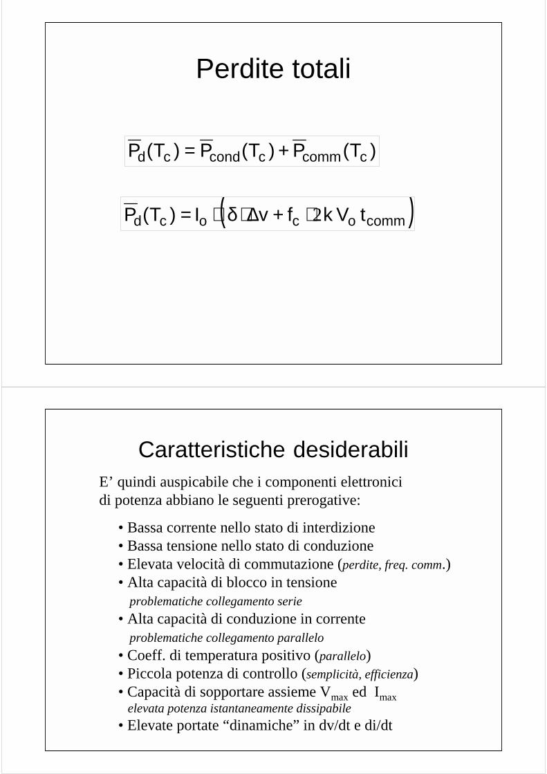
Perdite totali
)T(P)T(P)T(P ccommccondcd +=
( )commococd tVkfvI)T(P 2⋅+∆⋅δ⋅=
Caratteristiche desiderabiliE’ quindi auspicabile che i componenti elettronicidi potenza abbiano le seguenti prerogative:
• Bassa corrente nello stato di interdizione• Bassa tensione nello stato di conduzione• Elevata velocità di commutazione (perdite, freq. comm.)• Alta capacità di blocco in tensione
problematiche collegamento serie• Alta capacità di conduzione in corrente
problematiche collegamento parallelo• Coeff. di temperatura positivo (parallelo)• Piccola potenza di controllo (semplicità, efficienza)• Capacità di sopportare assieme Vmax ed Imax
elevata potenza istantaneamente dissipabile• Elevate portate “dinamiche” in dv/dt e di/dt

Caratteristiche componentiInterruttori statici di potenza
Vengono suddivisi in due lezioni:
parte (1)
Diodi
SCR
GTO
parte (2)
BJT
MOSFET
IGBT
Caratteristiche componenti (1)Diodi - SCR - GTO
Sono in assoluto quelli che presentano le piùelevate prestazioni in termini di portata in corrente e max. tensione sopportabile
Questi componenti fanno parte di una famiglia di dispositivi parzialmente controllabili in accensionee/o spegnimento
Le prime applicazioni di elettronica di potenza nascono alcune decine di anni fa proprio con questi dispositivi (SCR 1957)
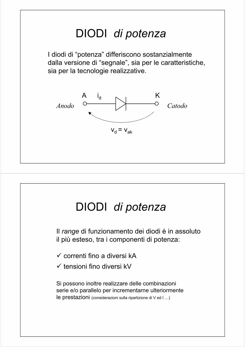
DIODI di potenza
I diodi di “potenza” differiscono sostanzialmentedalla versione di “segnale”, sia per le caratteristiche,sia per la tecnologie realizzative.
A KAnodo Catodo
id
vd = vak
DIODI di potenza
Il range di funzionamento dei diodi è in assolutoil più esteso, tra i componenti di potenza:
correnti fino a diversi kAtensioni fino diversi kV
Si possono inoltre realizzare delle combinazioniserie e/o parallelo per incrementarne ulteriormentele prestazioni (considerazioni sulla ripartizione di V ed I …)

DIODI di potenzaSi possono individuare tre tipologie di diodi:
Shottkybassissima Von (≅ 0.3 V)basse tensioni di lavoro (50÷100 V)
Fast-recovery (FRED)veloce reverse-recoverycentinaia di V ed A
Rectifiers (line frequency)raddrizzatori di retemigliaia di V ed A
DIODI di potenza
vak
id
VS
Ron
1
vak = Vs + Ron id
≅ 1V ≅ mΩ
-Vbr
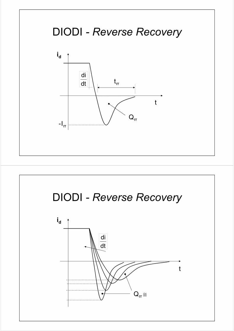
DIODI - Reverse Recovery
id
t
-Irr
trr
Qrr
dtdi
DIODI - Reverse Recovery
id
t
dtdi
Qrr ≅
TiristoriSCR - Silicon Controlled Rectifier
A K
G
Anodo Catodo
Gate
Sono dei diodi controllati in accensione
vd = vak
id
vGiG
SCR - Caratteristica on-off
vak
id
ILIH
IG = 0I’G > 0
VBOV’BO
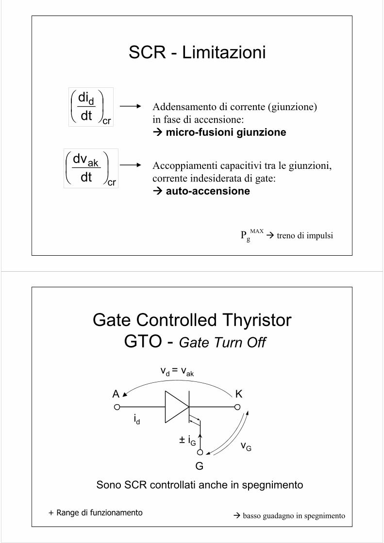
SCR - Limitazioni
cr
ddtdi
cr
akdt
dv
Addensamento di corrente (giunzione) in fase di accensione:
micro-fusioni giunzione
Accoppiamenti capacitivi tra le giunzioni,corrente indesiderata di gate:
auto-accensione
PgMAX treno di impulsi
Gate Controlled ThyristorGTO - Gate Turn Off
A K
G
Sono SCR controllati anche in spegnimento
vd = vak
id
± iG vG
basso guadagno in spegnimento+ Range di funzionamento
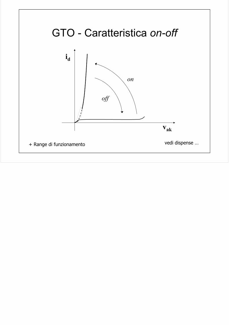
GTO - Caratteristica on-off
vak
id
off
on
vedi dispense …+ Range di funzionamento
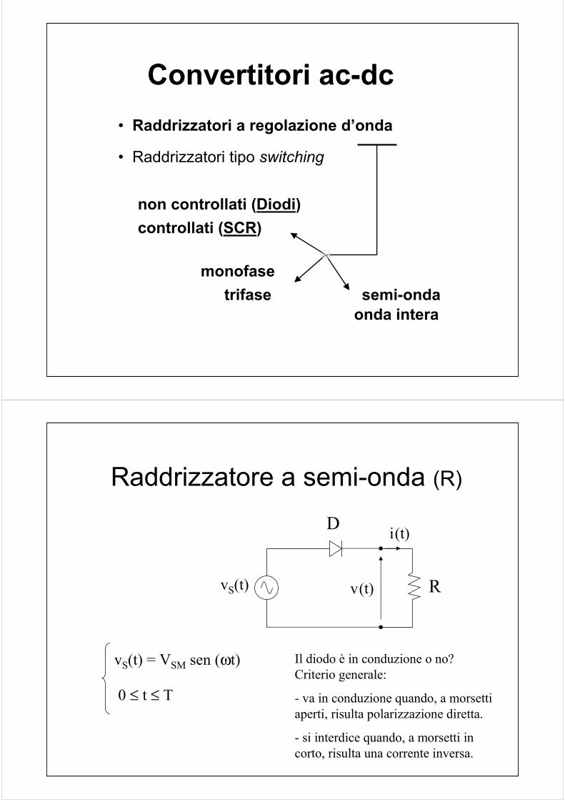
Convertitori ac-dc
non controllati (Diodi)controllati (SCR)
• Raddrizzatori a regolazione d’onda
• Raddrizzatori tipo switching
monofasetrifase semi-onda
onda intera
Raddrizzatore a semi-onda (R)
R
D
vS(t)
i(t)
v(t)
vS(t) = VSM sen (ωt)
0 ≤ t ≤ T
Il diodo è in conduzione o no?Criterio generale:
- va in conduzione quando, a morsetti aperti, risulta polarizzazione diretta.
- si interdice quando, a morsetti in corto, risulta una corrente inversa.
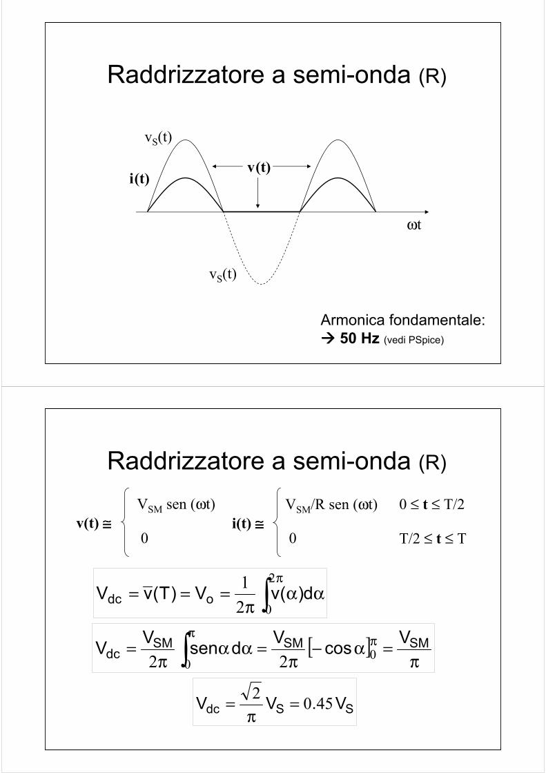
Raddrizzatore a semi-onda (R)
ωt
vS(t)
i(t)v(t)
vS(t)
Armonica fondamentale:50 Hz (vedi PSpice)
0 ≤ t ≤ T/2VSM sen (ωt)
0 T/2 ≤ t ≤ Tv(t) ≅≅≅≅ i(t) ≅≅≅≅
VSM/R sen (ωt)
0
∫π
ααπ
===2
021 d)(vV)T(vV odc
[ ]π
=α−π
=ααπ
= ππ
∫ SMSMSMdc
VcosVdsenVV 00 22
SSdc V.VV 4502 =π
=
Raddrizzatore a semi-onda (R)
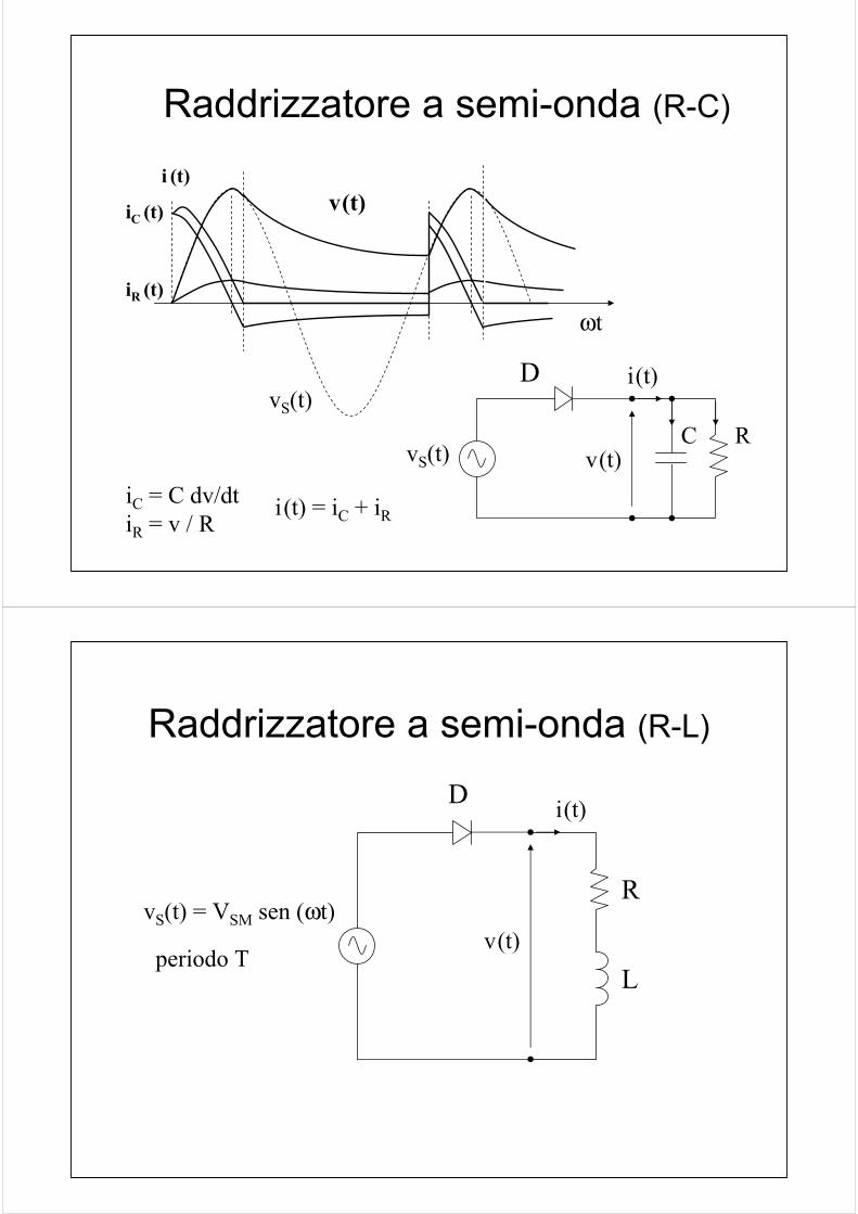
Raddrizzatore a semi-onda (R-C)
ωt
iC (t) v(t)
vS(t)R
D
vS(t)
i(t)
v(t)C
iR (t)
iC = C dv/dtiR = v / R
i(t) = iC + iR
i (t)
Raddrizzatore a semi-onda (R-L)
R
D i(t)
v(t)
L
vS(t) = VSM sen (ωt)
periodo T
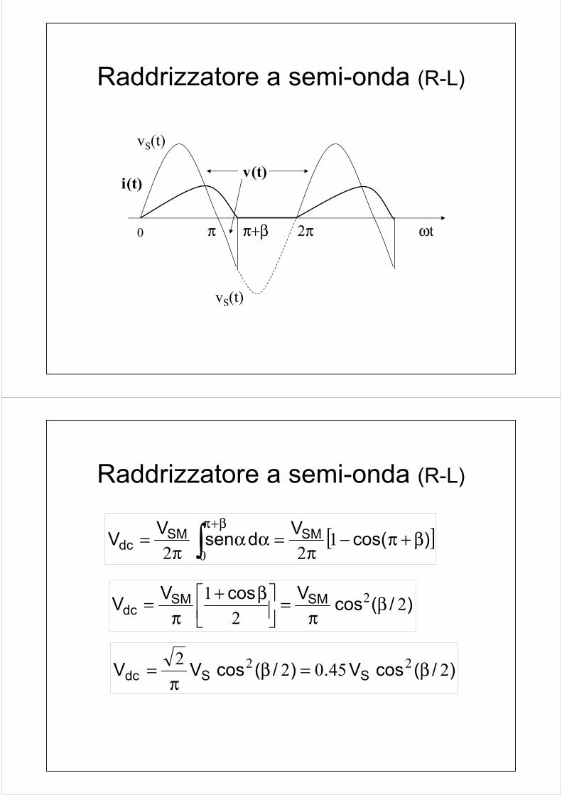
ωt
vS(t)
i(t)v(t)
vS(t)
Raddrizzatore a semi-onda (R-L)
0 π π+β 2π
Raddrizzatore a semi-onda (R-L)
[ ])cos(VdsenVV SMSMdc β+π−
π=αα
π= ∫
β+π1
22 0
)/(cosVcosVV SMSMdc 2
21 2 β
π=
β+
π=
)/(cosV.)/(cosVV SSdc 245022 22 β=βπ
=
Raddrizzatore a semi-onda (R-L)
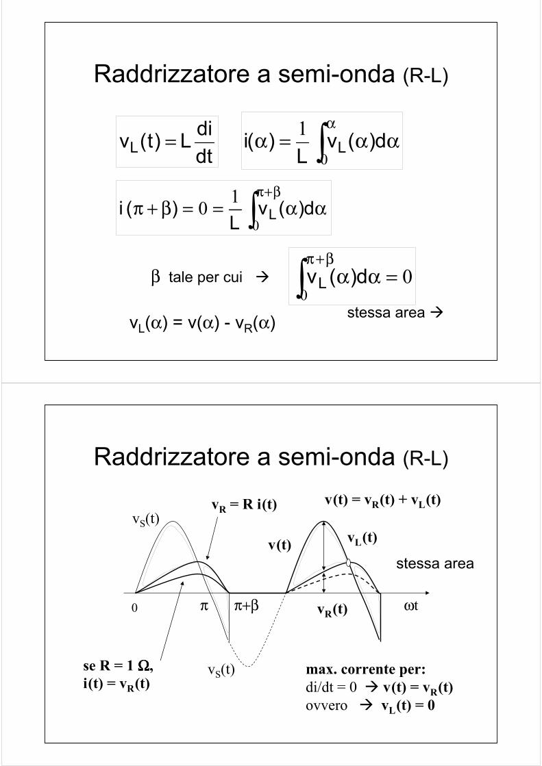
dtdiL)t(vL = ∫
ααα=α
0
1 d)(vL
)(i L
∫β+π
αα==β+π0
10 d)(vL
)( i L
00
=αα∫β+π
d)(vLβ tale per cui
stessa area vL(α) = v(α) - vR(α)
ωt
vS(t)vR = R i(t)
v(t)
vS(t)se R = 1 ΩΩΩΩ,i(t) = vR(t)
0 π π+β vR(t)
vL(t)
v(t) = vR(t) + vL(t)
Raddrizzatore a semi-onda (R-L)
stessa area
max. corrente per:di/dt = 0 v(t) = vR(t)ovvero vL(t) = 0
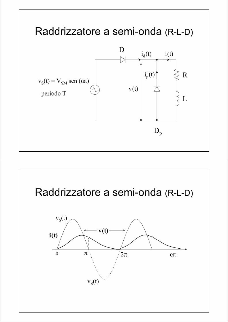
Raddrizzatore a semi-onda (R-L-D)
R
D i(t)
v(t)
L
vS(t) = VSM sen (ωt)
periodo T
Dp
id(t)
ip(t)
Raddrizzatore a semi-onda (R-L-D)
ωt
vS(t)
i(t)v(t)
vS(t)
0 π 2π
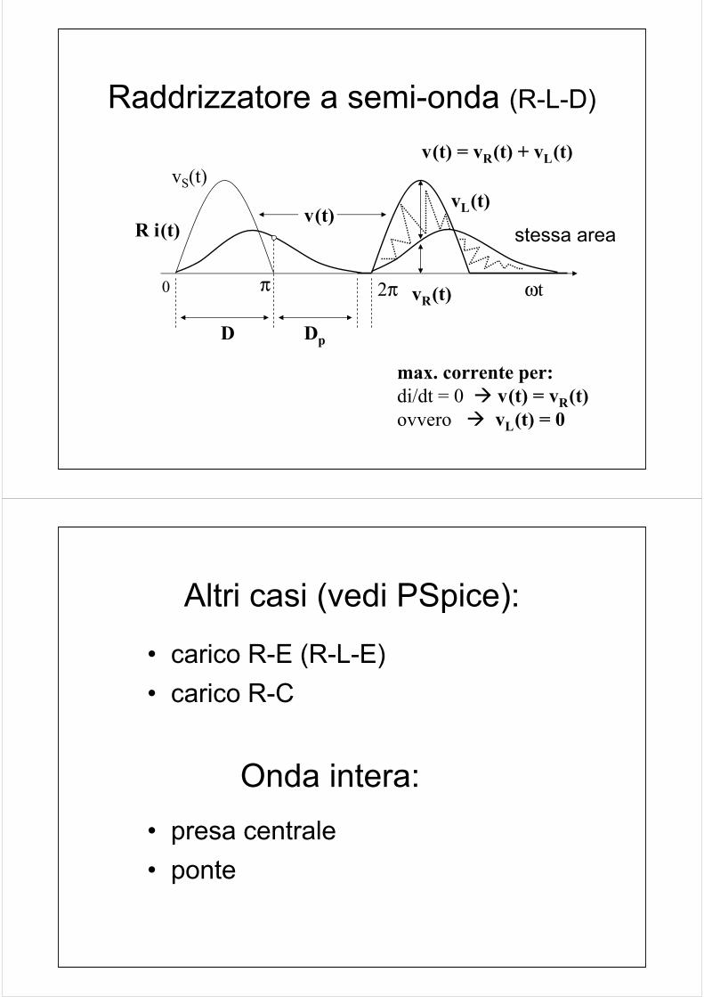
Raddrizzatore a semi-onda (R-L-D)
ωt
vS(t)
R i(t)v(t)
0 π 2π
D Dp
vR(t)
vL(t)
v(t) = vR(t) + vL(t)
stessa area
max. corrente per:di/dt = 0 v(t) = vR(t)ovvero vL(t) = 0
Altri casi (vedi PSpice):
• carico R-E (R-L-E)• carico R-C
• ponte• presa centrale
Onda intera:
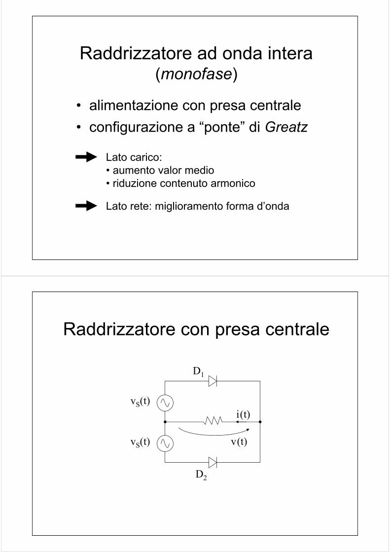
Raddrizzatore ad onda intera(monofase)
• configurazione a “ponte” di Greatz• alimentazione con presa centrale
Lato carico:• aumento valor medio• riduzione contenuto armonico
Lato rete: miglioramento forma d’onda
Raddrizzatore con presa centrale
D1
vS(t)i(t)
v(t)
D2
vS(t)

Raddrizzatore a ponte (R)
R
D1
vS(t)
i(t)
v(t)D2
D3
D4
Lavagna: altre disposizioni dei lati
Raddrizzatore ad onda intera (R)
ωt
vS(t)
i(t)
v(t)
vS(t)
iS(t)
Armonica principale:100 Hz

0 ≤ t ≤ T/2VSM sen (ωt)
T/2 ≤ t ≤ Tv(t) ≅≅≅≅ i(t) ≅≅≅≅
VSM/R sen (ωt)
∫π
ααπ
===2
021 d)(vV)T(vV odc
[ ] SMSMSM
dc VcosVdsenVVπ
=α−π
=ααπ
= ππ
∫ 222 0
0
SSdc V.VV 90022 =π
=
-VSM sen (ωt) -VSM/R sen (ωt)
Raddrizzatore ad onda intera (R)
Raddrizzatore ad onda intera
Considerazioni sullo spettro armonicoe sui filtri lato continua
Altri casi (vedi PSpice):
• carico RL, RE, RLE, RC• carico Idc = cost• correnti lato rete
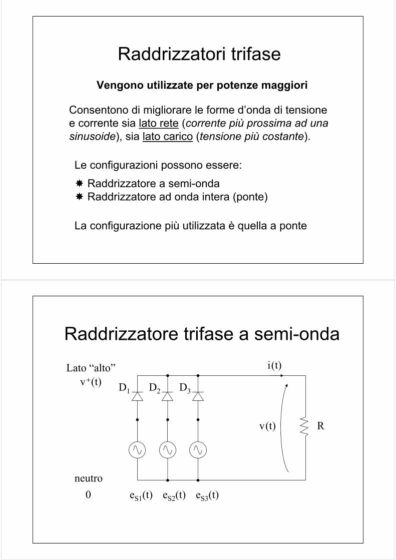
Raddrizzatori trifaseVengono utilizzate per potenze maggiori
Consentono di migliorare le forme d’onda di tensionee corrente sia lato rete (corrente più prossima ad unasinusoide), sia lato carico (tensione più costante).
La configurazione più utilizzata è quella a ponte
Le configurazioni possono essere:
Raddrizzatore a semi-ondaRaddrizzatore ad onda intera (ponte)
Raddrizzatore trifase a semi-onda
D1
i(t)
v(t)
D2 D3
R
eS1(t) eS2(t) eS3(t)
Lato “alto”v+(t)
neutro0

La conduzione avviene per il diodo con l’anodocollegato al morsetto di rete che presenta il maggior potenziale, ovvero, la maggior tensione stellata
v(t) = v+(t) = maxeSk (t)
conduce il diodo fase k
Raddrizzatore trifase a semi-onda
La tensione di uscita risulta l’inviluppo delle eSk (t)
ωt
eS1(t)
v+(t)
eS2(t) eS3(t)
2/3π
0
v(t)
Raddrizzatore trifase a semi-onda
Armonica fondamentale:150 Hz

Ne consegue che ogni diodo conduce per 1/3 di periodo:
°⇔π⇔ 12032
3Tconduzione
per diodo
Si ha in questo caso la conduzione di un solo diodoalla volta. Il funzionamento è assimilabile a quello del raddrizzatore monofase con presa centrale.
Raddrizzatore trifase a semi-onda
Un’eventuale L nel carico non influenza la conduzione dei diodi
Un’eventuale L lato rete influenza la conduzione dei diodi
Esaminare le varie casistiche:
• carico R-E
• carico R-L (calcolo correnti medie)
• carico Io
• carico R-L-E
Raddrizzatore trifase a semi-onda
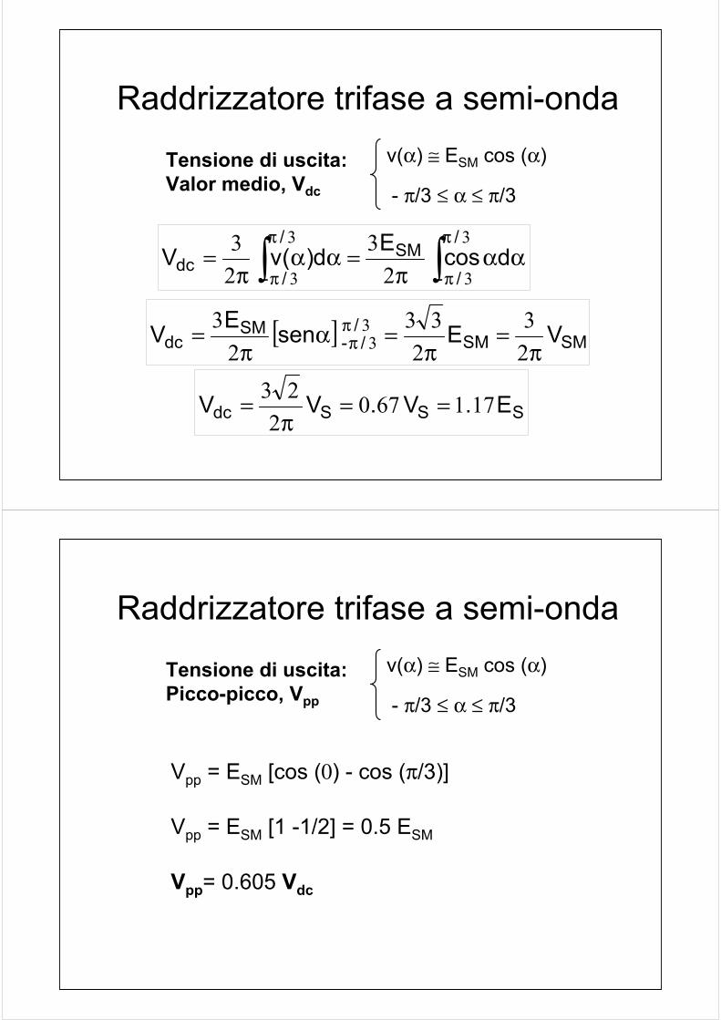
- π/3 ≤ α ≤ π/3
v(α) ≅ ESM cos (α)
∫∫π
π
π
παα
π=αα
π=
3
3
3
3 23
23 /
/-SM
/
/-dc dcosEd)(vV
[ ] SMSM/ /-
SMdc VEsenEV
π=
π=α
π= π
π 23
233
23 3
3
SSSdc E.V.VV 1716702
23 ==π
=
Tensione di uscita:Valor medio, Vdc
Raddrizzatore trifase a semi-onda
- π/3 ≤ α ≤ π/3
v(α) ≅ ESM cos (α)Tensione di uscita:Picco-picco, Vpp
Vpp = ESM [cos (0) - cos (π/3)]
Vpp = ESM [1 -1/2] = 0.5 ESM
Vpp= 0.605 Vdc
Raddrizzatore trifase a semi-onda
ωt
eS1(t)
2/3π
0
v(t)
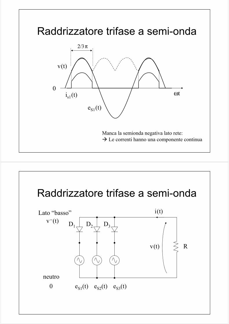
Raddrizzatore trifase a semi-onda
is1(t)
Manca la semionda negativa lato rete:Le correnti hanno una componente continua
Raddrizzatore trifase a semi-onda
D1
i(t)
v(t)
D2 D3
R
eS1(t) eS2(t) eS3(t)
Lato “basso”v−(t)
neutro0

La conduzione avviene per il diodo con il catodocollegato al morsetto di rete che presenta il minor potenziale, ovvero, la minor tensione stellata
v(t) = v−(t) = mineSk (t)
conduce il diodo fase k
Raddrizzatore trifase a semi-onda
La tensione di uscita risulta l’inviluppo delle −eSk (t)
ωt
eS1(t)
v−(t)
eS2(t) eS3(t)
2/3π
0
v(t)
Raddrizzatore trifase a semi-onda
Armonica fondamentale:150 Hz
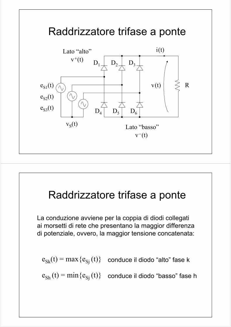
D1
vS(t)
i(t)
v(t)
D2 D3
D4 D5 D6
ReS1(t)
eS2(t)
eS3(t)
Lato “alto”
Lato “basso”
v+(t)
v−(t)
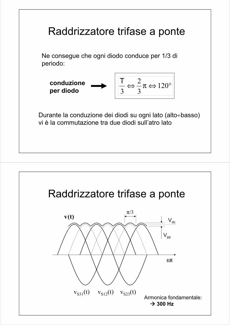
Raddrizzatore trifase a ponte
Raddrizzatore trifase a ponte
La conduzione avviene per la coppia di diodi collegati ai morsetti di rete che presentano la maggior differenza di potenziale, ovvero, la maggior tensione concatenata:
eSk(t) = maxeSj (t)
eSh (t) = mineSj (t)
conduce il diodo “alto” fase k
conduce il diodo “basso” fase h

Raddrizzatore trifase a ponte
ωt
eS1(t)
v+(t)
eS2(t)eS3(t)
2/3π
v−(t)
v(t)
Raddrizzatore trifase a ponte
D1
vS(t)
i(t)
v(t)
D2 D3
D4 D5 D6
ReS1(t)
eS2(t)
eS3(t)
v(t) = eS1(t) – eS3(t)= vS13(t)
eS1 = maxeSjeS3 = mineSj
Esempio:
Raddrizzatore trifase a ponte
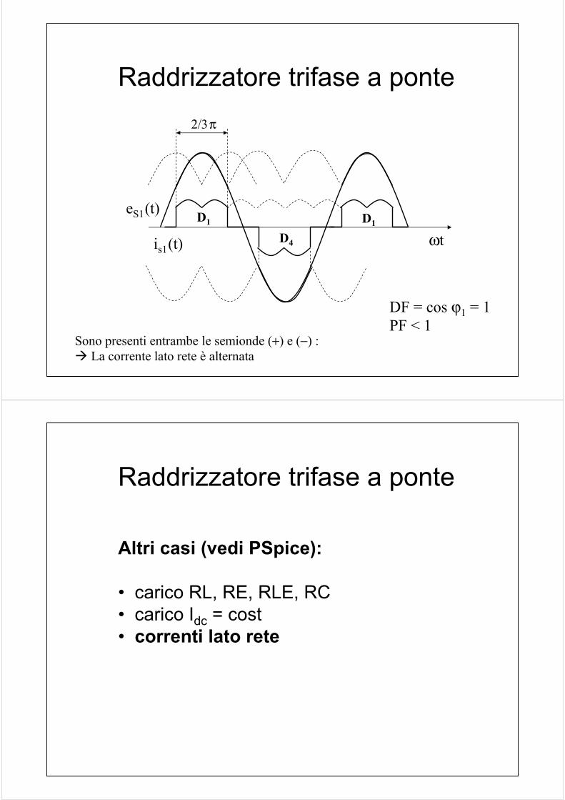
Ne consegue che ogni diodo conduce per 1/3 di periodo:
conduzioneper diodo
Durante la conduzione dei diodi su ogni lato (alto÷basso)vi è la commutazione tra due diodi sull’atro lato
°⇔π⇔ 12032
3T
ωt
vS12(t)
v(t)
vS23(t)Armonica fondamentale:
300 Hz
Vpp
π/3
vS31(t)
Raddrizzatore trifase a ponte
Vdc

- π/6 ≤ α ≤ π/6
v(α) ≅ VSM cos (α)
∫∫π
π
π
παα
π=αα
π=
6
6
6
6 331 /
/-SM
/
/-dc dcos
/Vd)(v
/V
Raddrizzatore trifase a ponte
[ ] SMSM/ /-
SMdc V.Vsen
/VV 95503
366 =
π=α
π= π
π
SSdc V.VV 35123 =π
=
Tensione di uscita:Valor medio, Vdc
Raddrizzatore trifase a ponte
- π/6 ≤ α ≤ π/6
v(α) ≅ VSM cos (α)Tensione di uscita:Picco-picco, Vpp
Vpp = VSM [cos (0) - cos (π/6)]
Vpp = VSM [1 -√3/2] = 0.134 VSM
Vpp= 0.141 Vdc
Raddrizzatore trifase a ponte
ωt
eS1(t)
2/3π
DF = cos ϕ1 = 1PF < 1
is1(t)
Sono presenti entrambe le semionde (+) e (−) :La corrente lato rete è alternata
D1D4
D1
Altri casi (vedi PSpice):
• carico RL, RE, RLE, RC• carico Idc = cost• correnti lato rete
Raddrizzatore trifase a ponte
Raddrizzatori controllati• I Diodi sono sostituiti da SCR
• viene controllato (ritardandolo) l’istante di innesco
• lo spegnimento avviene come per i Diodi (“naturale”)
il valor medio della tensione lato dc può esseresolo abbassato (rispetto al caso di raddrizzatorenon controllato a Diodi)
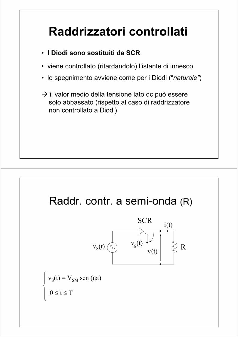
Raddr. contr. a semi-onda (R)
R
SCR
vS(t)
i(t)
v(t)
vS(t) = VSM sen (ωt)
0 ≤ t ≤ T
vg(t)

Raddr. contr. a semi-onda (R)
ωt
vS(t)
i(t)
v(t)
vS(t)
0 πα∗
vg(t)
2π
0 t∗ tTT/2 T+ t∗
t* ≤ t ≤ T/2VSM sen (ωt)
0 T/2 ≤ t ≤ T+ t*v(t) ≅≅≅≅ i(t) ≅≅≅≅
VSM/R sen (ωt)
0
∫π
ααπ
===2
021 d)(vV)T(vV odc
[ ]πα
π
αα−
π=αα
π= ∫ *
SM*
SMdc cosVdsenVV
22
221 2 *cos
V*cosVV SMSM
dcα
π=α+
π=
Raddr. contr. a semi-onda (R)
α* < π
non controllato

R
SCR i(t)
v(t)
L
vS(t) = VSM sen (ωt)
periodo T
vg(t)
Raddr. contr. a semi-onda (R-L)
ωt
vS(t)
i(t)
v(t)
vS(t)
Raddr. contr. a semi-onda (R-L)
0 π π+β 2π
stessa area(R=1ΩΩΩΩ)
α∗
vR(t)

α+β
π=αα
π= ∫
β+π
α 22*coscosVdsenVV SM
*SM
dc
Raddr. contr. a semi-onda (R-L)
22β−αβ+α
π= *cos*cosVV SM
dc
non controllato
Raddr. contr. a semi-onda (altri)
Considerazioni analoghe al caso di raddrizzatore non controllato per:
• carico R-E (R-L-E)
• carico R-C
• diodo di libera circolazione
Vedi esercitazioni PSpice

Raddr. contr. ad onda intera (R)
R
S1
vS(t)
i(t)
v(t)S2
S3
S4
Raddr. contr. ad onda intera (R)
RvS(t)
i(t)
v(t)
S1 S3
S2 S4
Rappresentazione a rami

Raddr. contr. ad onda intera (R)
ωt
vS(t)
i(t)
v(t)
0 πα∗
vg(t)
2π
0 t∗ tTT/2S1-S4 S2-S3
T+ t∗T/2+ t∗
S1-S4Se il controllo non è simmetrico
f1 = 50 Hz invece di 100 Hz
Raddr. contr. ad onda intera (R)
∫π
ααπ
===0
1 d)(vV)T(vV odc
[ ]πα
π
αα−
π=αα
π= ∫ *
SM*
SMdc cosVdsenVV
22
212 2 *cosV*cosVV SMSMdc
απ
=α+π
=
non controllato
Raddr. contr. ad onda intera (R-L)
ωt
vS(t)
i(t)
v(t)
0 πα∗ 2ππ+α∗
modo “continuo”
iS(t)
controllo completo Vdc
Raddr. contr. ad onda intera (R-L)
non controllato
[ ] **
SM*
*SM
dc cosVdsenVV α+πα
α+π
αα−
π=αα
π= ∫
[ ] *cosV*)cos(*cosVV SMSMdc απ
=α+π−απ
= 21
0 ≤ α* ≤ π
tensione lato dc (++++) o (−−−−)solo in transitorio se il carico non è attivo
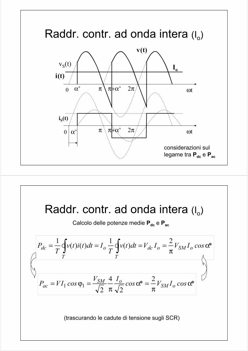
Raddr. contr. ad onda intera (Io)
ωt
vS(t)
i(t)
v(t)
0 πα∗ 2ππ+α∗
iS(t)
ωt0 πα∗ 2ππ+α∗
considerazioni sul legame tra Pdc e Pac
Io
Raddr. contr. ad onda intera (Io)Calcolo delle potenze medie Pdc e Pac
*cosIVIVdttvT
IdttitvT
P oSModc
T
o
T
dc απ
==== ∫∫ 2 )(1 )()(1
*cosIV*cosIVcosIVP oSMoSM
ac απ
=απ
=ϕ= 22
42
11
(trascurando le cadute di tensione sugli SCR)
Raddr. contr. ad onda intera (R-L)
Considerazioni analoghe al caso di raddrizzatore non controllato per:
• carico R-E (R-L-E)
• carico R-C attenzione ai dv/dt !
• diodo di libera circolazione
Vedi esercitazioni PSpice
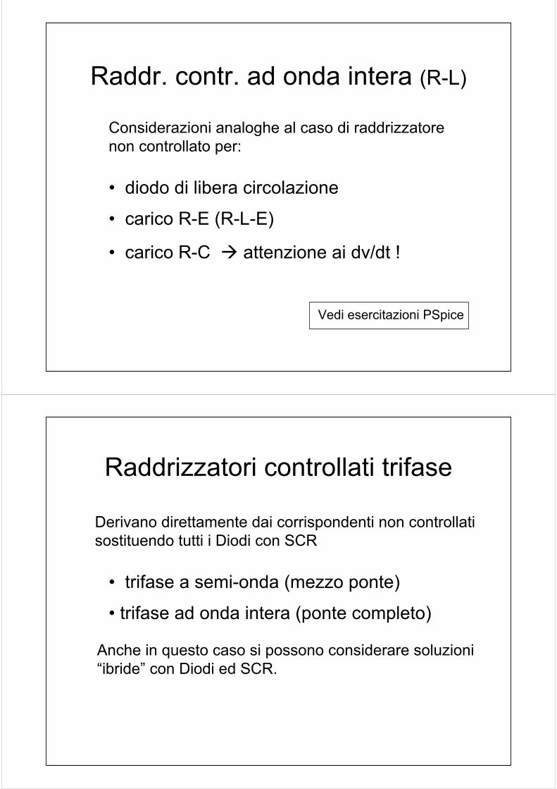
Raddrizzatori controllati trifase
Derivano direttamente dai corrispondenti non controllatisostituendo tutti i Diodi con SCR
• trifase ad onda intera (ponte completo)
• trifase a semi-onda (mezzo ponte)
Anche in questo caso si possono considerare soluzioni“ibride” con Diodi ed SCR.

Raddrizzatori controllati trifasesemi-onda
S1
i(t) = Idc
v(t)
S2 S3
Idc
eS1(t) eS2(t) eS3(t)
Lato “alto”v+(t)
neutro0
Raddrizzatori controllati trifasesemi-onda
ωt
eS1(t)
v+(t)
eS2(t) eS3(t)
2/3π
0
v(t)
π 2π
π/6+α∗ 5/6π+α∗
Vdc= 3√3 /2π ESM cos α∗

Raddrizzatori controllati trifaseonda intera
S1
v(t)
S2 S3
S4 S5 S6
eS1(t)
eS2(t)
eS3(t)
i(t) = Idc
Idc
Vdc= 3√3 /π ESM cos α∗ = 3 /π VSM cos α∗
Raddrizzatori controllati trifase
onda intera

Caratteristiche componentiInterruttori statici di potenza
Vengono suddivisi in due lezioni:
parte (1)
Diodi
SCR
GTO
parte (2)
BJT
MOSFET
IGBT
Caratteristiche componenti (2)BJT – MOSFET - IGBT
Le prestazioni in termini di portata in corrente e max. tensione sopportabile sono più modeste.
Questi componenti fanno parte di una famiglia di dispositivi totalmente controllabili, sia in accensioneche in spegnimento.
Per contro, facilità di controllo e velocità di commutazione costituiscono il punto di forza per questi dispositivi.
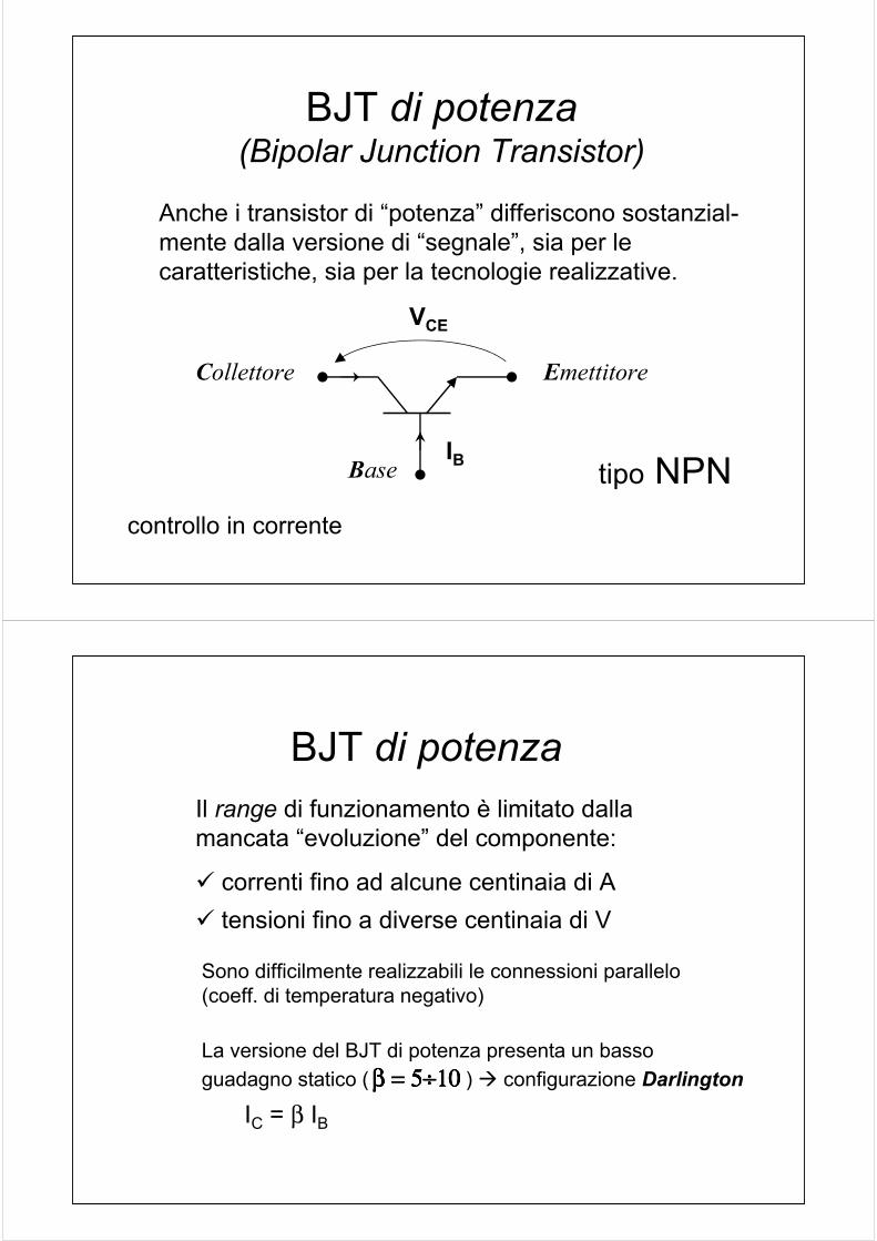
BJT di potenza(Bipolar Junction Transistor)
Anche i transistor di “potenza” differiscono sostanzial-mente dalla versione di “segnale”, sia per le caratteristiche, sia per la tecnologie realizzative.
Collettore Emettitore
Base tipo NPN
VCE
IB
controllo in corrente
Il range di funzionamento è limitato dallamancata “evoluzione” del componente:
correnti fino ad alcune centinaia di Atensioni fino a diverse centinaia di V
Sono difficilmente realizzabili le connessioni parallelo(coeff. di temperatura negativo)
BJT di potenza
La versione del BJT di potenza presenta un bassoguadagno statico ( β = 5β = 5β = 5β = 5÷÷÷÷10101010 ) configurazione Darlington
IC = β IB

BJT di potenzaConfigurazione Darlington C
B
E
β1
β2
IE = IE2 ≅ β2 IE1
≅ β2 β1 IB1
IE ≅ βtot IB
βtot = β1 β2
β1 ≅ 10÷20β2 ≅ 5÷10
βtot ≅ 50 ÷200
BJT di potenza (I-V)
VCE
IC
IB = 0
IB > 0
interdizione
saturazionespinta (hard)
quasi-saturazione(soft)
retta dicarico
zona attiva
(vedi: Baker’s clamp)
diodo extra per spegnimento veloce
BJT di potenza
C
B
Baker’s clamp:
E
D1 D2
D3
D4
VCEsat = VBE + VD1 + VD2 + …. - VD4
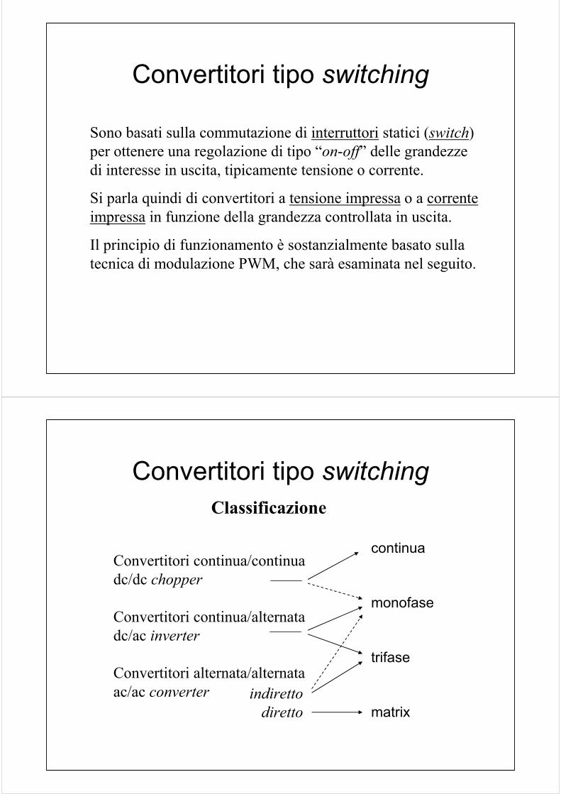
MOSFET(Metal-Oxide-Semiconductor
Field-effect Transistor)Si possono presentare nelle 4 configurazioni tipiche:
canale P÷N , arricchimento÷svuotamento
Drain Source
Gate canale N
VDS
VGS
arricchimentocontrollo in tensione
body diode

MOSFET
Promemoria argomenti:
• ingresso capacitivo (≈ nF) driver, Kelvin source
• uscita resistiva, Ron ≈ k VDS2.5 , parallelo
• caratteristiche body-diode
• caratteristica statica, range V-I
• caratteristiche dinamiche
IGBT(Insulated Gate Bipolar Transistor)
Costituiscono un ibrido tra il BJT, nello stadio di potenza,ed il MOSFET, nello parte di controllo:
Collettore Emettitore
Gate tipo NPN
VCE
VGE
controllo in tensione

IGBT
Promemoria argomenti:
• ingresso capacitivo, vedi MOSFET
• uscita tipo BJT
• assenza del body-diode
• caratteristiche statiche e dinamiche ibride
Cenni sui nuovi componenti emergenti: MCT
Convertitori tipo switching
Sono basati sulla commutazione di interruttori statici (switch) per ottenere una regolazione di tipo “on-off” delle grandezze di interesse in uscita, tipicamente tensione o corrente.
Si parla quindi di convertitori a tensione impressa o a corrente impressa in funzione della grandezza controllata in uscita.
Il principio di funzionamento è sostanzialmente basato sulla tecnica di modulazione PWM, che sarà esaminata nel seguito.
Convertitori tipo switching
Convertitori continua/continuadc/dc chopper
Convertitori continua/alternatadc/ac inverter
Convertitori alternata/alternataac/ac converter
monofase
trifase
continua
Classificazione
matrixindiretto
diretto
Convertitori dc/dc tipo switching
Step-down converter (chopper buck, abbassatore)
Step-up converter (chopper boost, innalzatore)
Step-down/step-up converter (chopper buck-boost)
Cùk converter (abbassatore/innalzatore)
Full bridge converter (ponte ad H, inverter monofase)
Sono chiamati chopper (spezzettatore) in quanto basati sulla regolazione ad intermittenza “on-off”.
Le tipologie di convertitori dc/dc più diffuse sono:

La modulazione a larghezza di impulso
Pulse Width Modulation (PWM)
Introduzione Con la modulazione PWM il convertitore può generare in uscita una prefissata forma d’onda del segnale di tensione (o corrente) La modulazione consiste sostanzialmente in due fasi:– discretizzazione temporale– riproduzione “on/off” del valor medio
La determinazione del ciclo on/off può essere per via numerica o analogica.
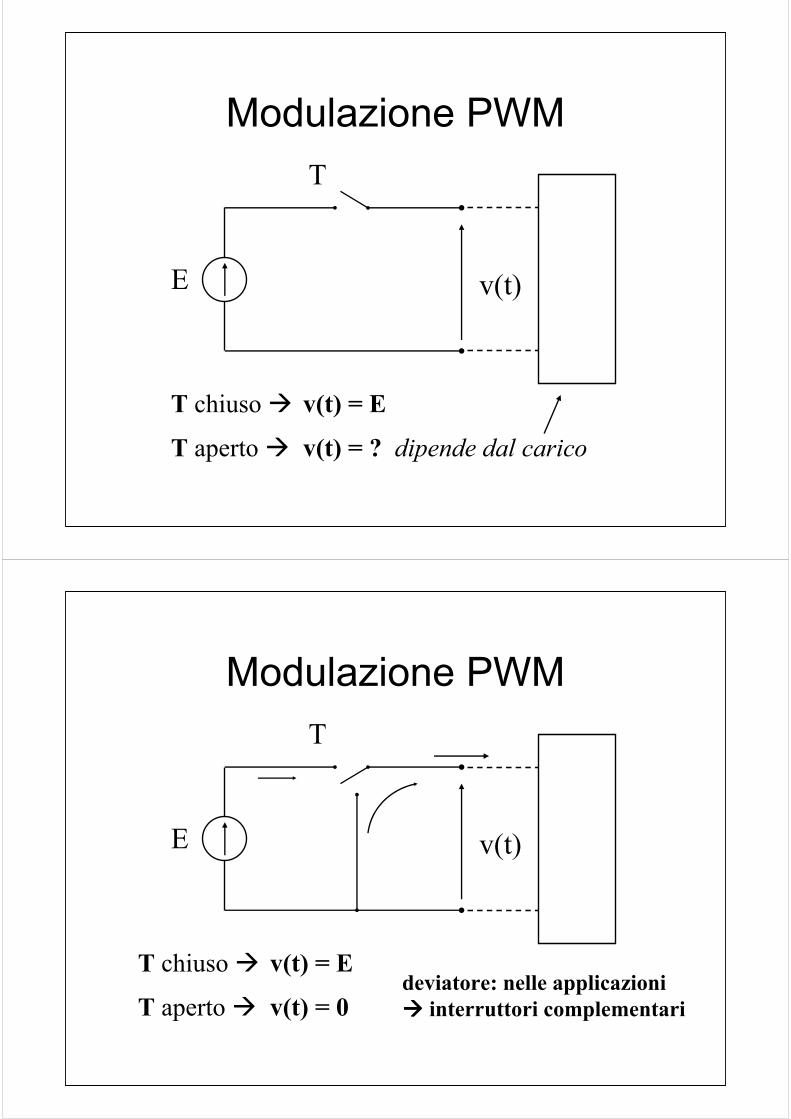
Modulazione PWM
E
T
v(t)
T chiuso v(t) = E
T aperto v(t) = ? dipende dal carico
Modulazione PWM
E
T
v(t)
T chiuso v(t) = E
T aperto v(t) = 0deviatore: nelle applicazioni
interruttori complementari
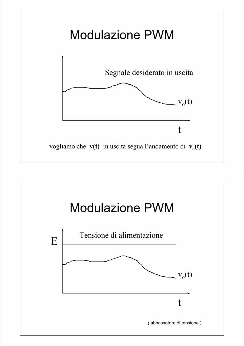
Modulazione PWM
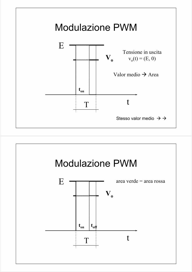
vo(t)
t
Segnale desiderato in uscita
vogliamo che v(t) in uscita segua l’andamento di vo(t)
Modulazione PWM
E
vo(t)
t
Tensione di alimentazione
( abbassatore di tensione )

Modulazione PWM
E
vo(t)
t
Suddivisione del tempo in intervalli
Possiamo considerare la tensione di uscita v(t)“soddisfacente” se segue il valor medio della
tensione desiderata vo(t) in ciascuno di questi intervalli
Modulazione PWM
E
vo(t)
tT“ciclo” o “periodo”

Modulazione PWM
EVo
tT
imponiamo in uscita lo stesso valor medio:
vo(T) = Vo = v(T)
Modulazione PWM
EVo
tT
Valor medio Area
Tensione desiderata, Vo
Modulazione PWM
EVo
tT
ton
Valor medio Area
Tensione in uscitavo(t) = (E, 0)
Stesso valor medio
Modulazione PWM
EVo
tT
ton toff
area verde = area rossa
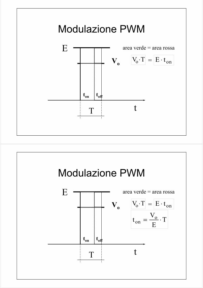
Modulazione PWM
EVo
tT
ton toff
area verde = area rossa
V To ⋅ E ton⋅=
Modulazione PWM
EVo
tT
ton toff
t VE
Tono= ⋅
area verde = area rossa
V To ⋅ E ton⋅=
Modulazione PWM
tTEon o= ⋅ V
Tali relazioni possono essere implementate digitalmente:
• mediante un microprocesssore (DSP) per il calcolo• con un timer per la temporizzazione
In questo modo è possibile controllare gli intervallidi accensione e spegnimento dell’interruttore.
t T toff on= −
Modulazione PWM
La relazione lineare tra il tempo di accensione (ton)ed il valore della tensione di uscita desiderata (Vo)suggerisce una modalità per una implementazioneanalogica della tecnica PWM.
tTEon o= ⋅ V t T toff on= −

Modulazione PWM
EVo
tT
Portante a dente di segaVp(t)
Modulazione PWM
EVo
tT
ton
Interruttore “on” se:
V V to p> ( )
Vp(t)
Modulazione PWM
EVo
tT
toffVp(t)Interruttore “off” se:
V V to p< ( )
Modulazione PWM
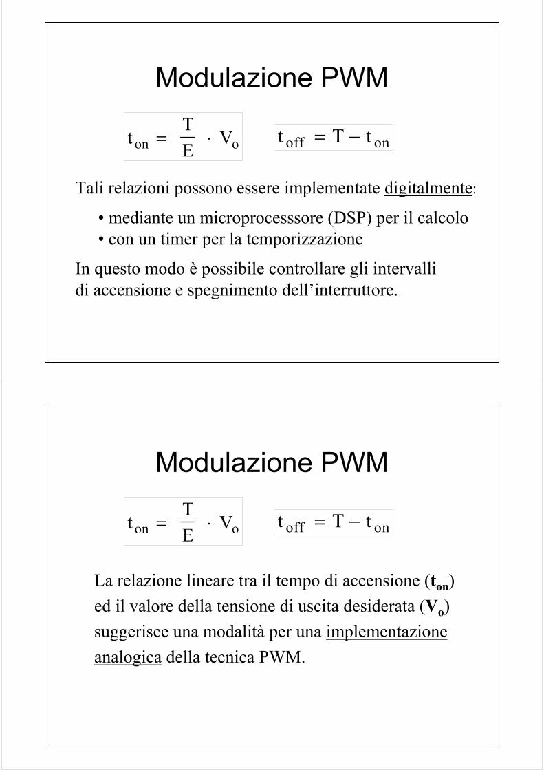
EVo
tT
ton
toffVp(t)
Interruttore “on” se:
V V to p> ( )
Interruttore “off” se:
V V to p< ( )
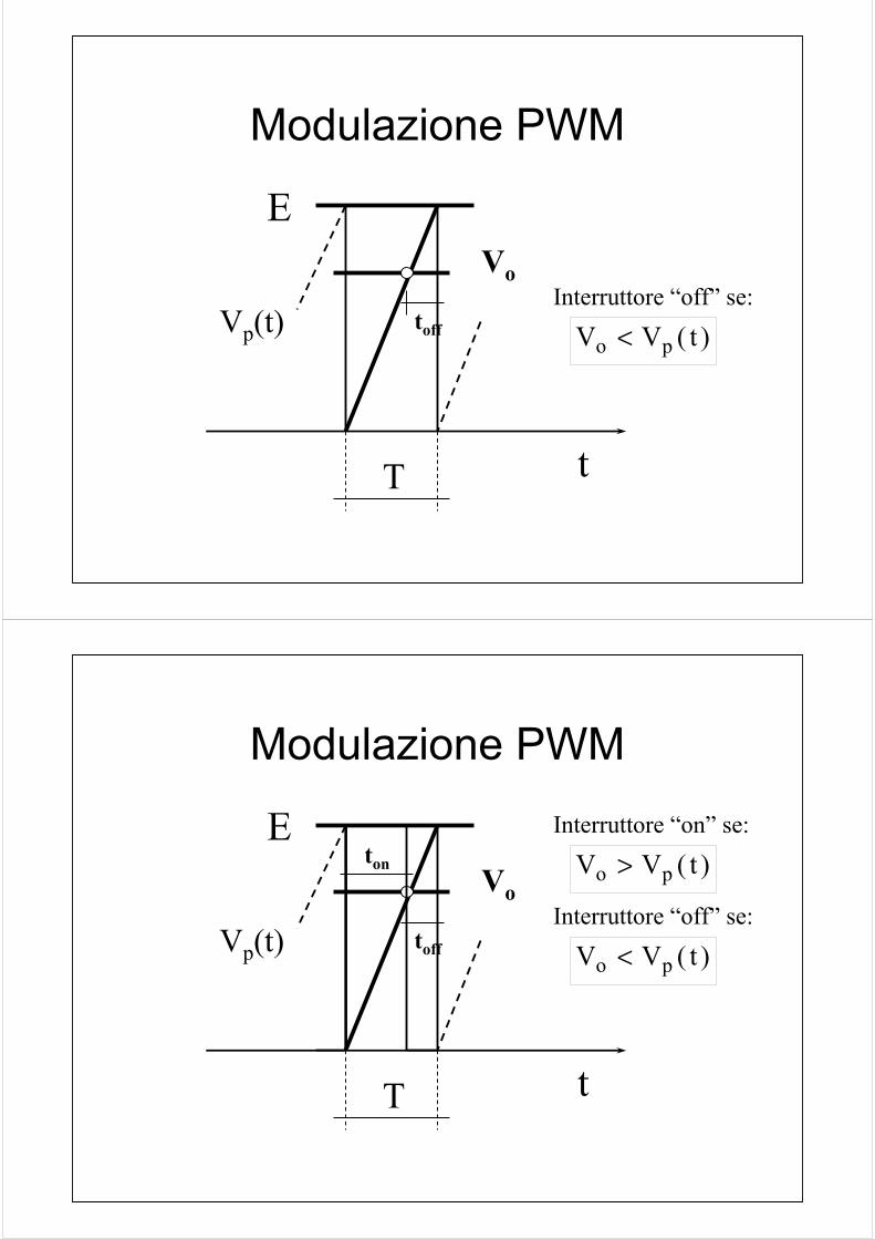
Modulazione PWM
t
ton
Vo
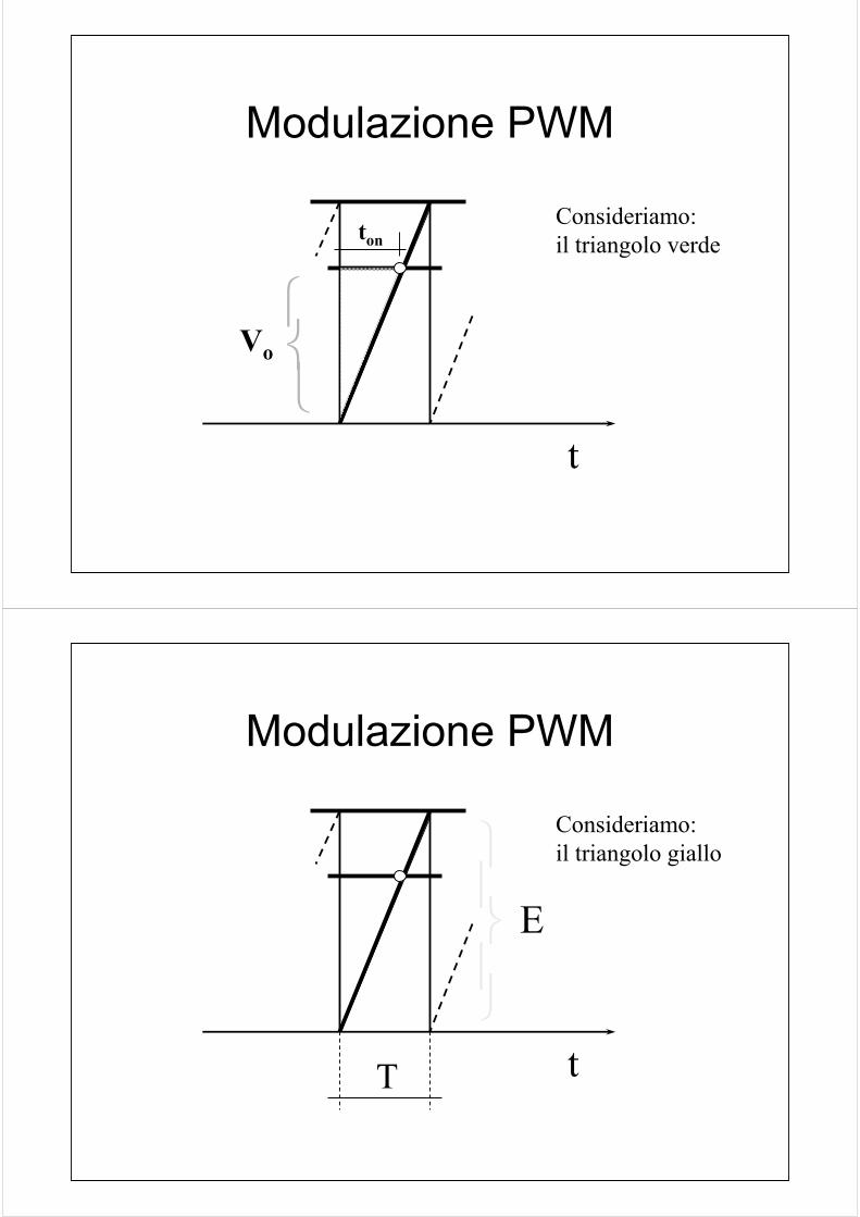
Consideriamo:il triangolo verde
Modulazione PWM
E
tT
Consideriamo:il triangolo giallo

Modulazione PWM
E
t
ton
Vo
Triangoli simili:
T
Modulazione PWM
E
t
ton
Vo
Triangoli simili:
tVon
o
TE
=
T

Modulazione PWM
E
t
ton
Vo
Triangoli simili:
t VE
Tono= ⋅
T
tVon
o
TE
=
Modulazione PWM
E
Vo(t)
tT
modulazione con portante a “dente di sega”
Modulazione PWM
E
vo(t)
t
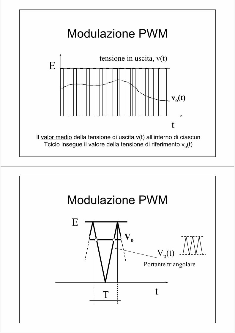
tensione in uscita, v(t)
Il valor medio della tensione di uscita v(t) all’interno di ciascun Tciclo insegue il valore della tensione di riferimento vo(t)
Modulazione PWM
EVo
tT
Portante triangolareVp(t)
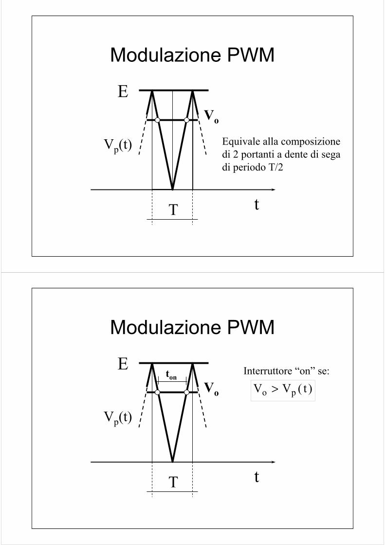
Modulazione PWM
EVo
tT
Equivale alla composizionedi 2 portanti a dente di segadi periodo T/2
Vp(t)
Modulazione PWM
EVo
tT
Interruttore “on” se:
V V to p> ( )ton
Vp(t)

Modulazione PWM
EVo
tT
Interruttore “off” se:
V V to p< ( )Vp(t) toff
Modulazione PWM
EVo
tT
Interruttore “on” se:
V V to p> ( )
Interruttore “off” se:
V V to p< ( )Vp(t) toff
ton
Modulazione PWM
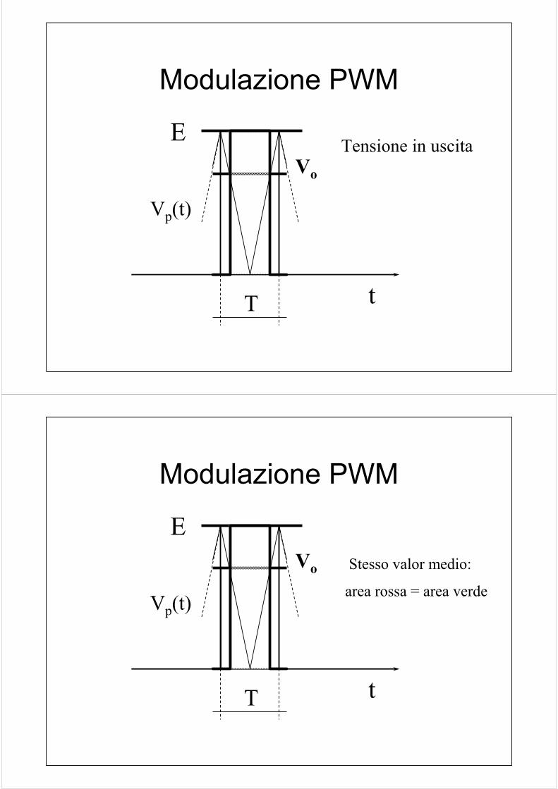
EVo
tT
Vp(t)
Tensione in uscita
Modulazione PWM
EVo
tT
Vp(t)area rossa = area verde
Stesso valor medio:
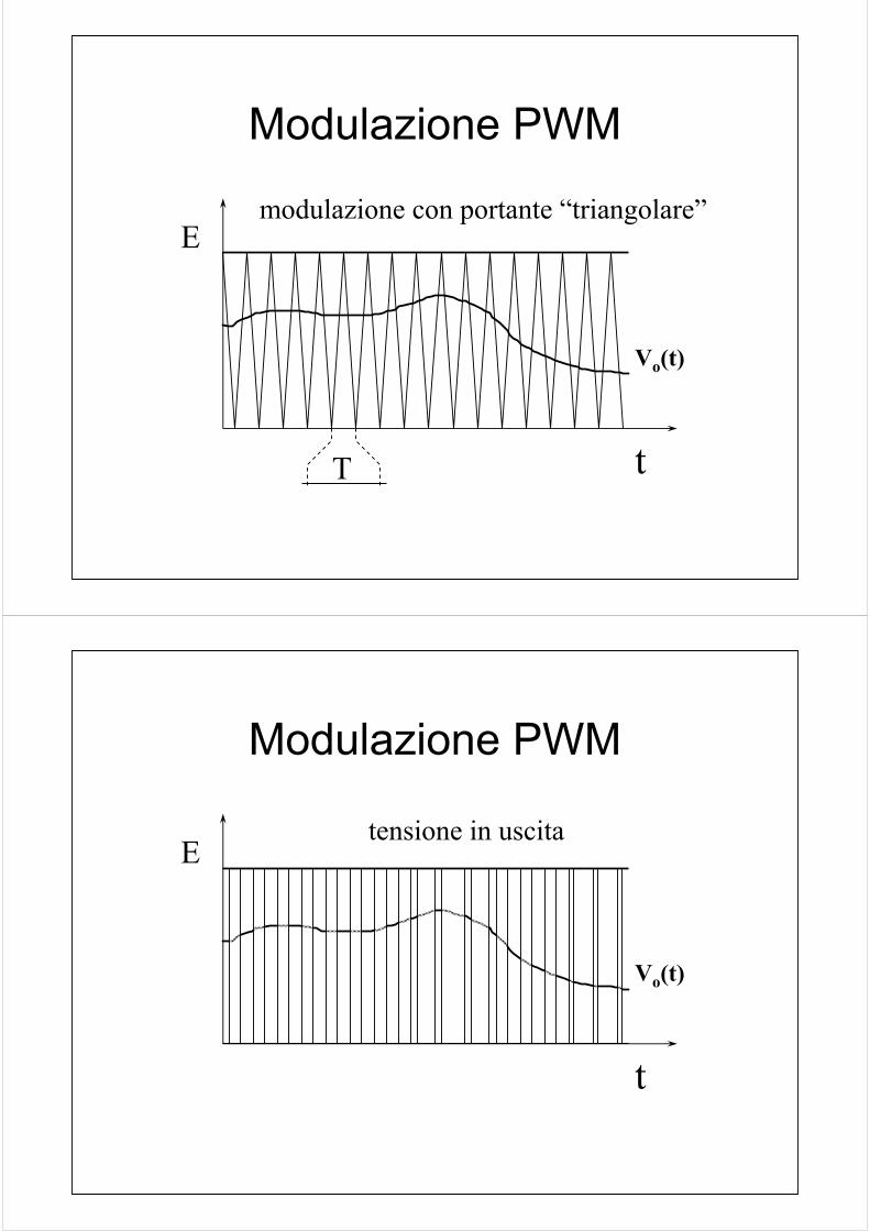
Modulazione PWM
E
Vo(t)
tT
modulazione con portante “triangolare”
Modulazione PWM
E
Vo(t)
t
tensione in uscita

Modulazione PWMContenuto armonico
Vk
fc = 1/T 2fc 3fc
disturbo
segnale utilef
- esempio con vo(t) = cost- filtro passa-basso
Modulazione PWM
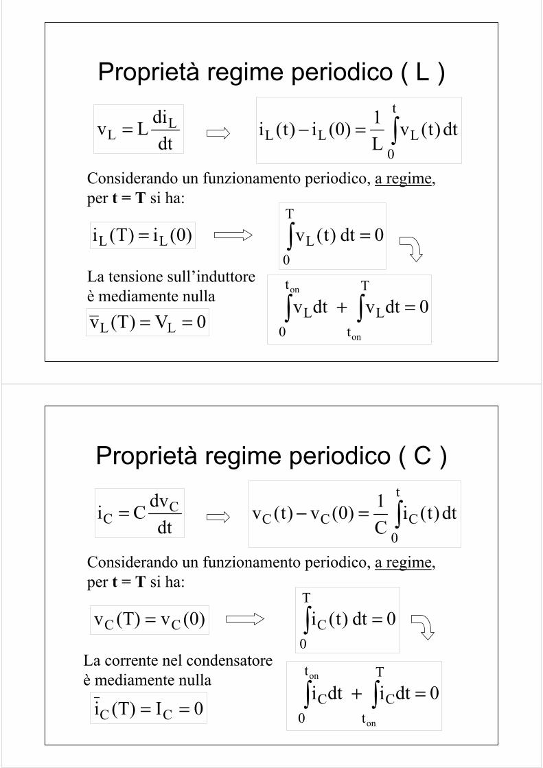
Proprietà regime periodico ( L )
dtdiLv L
L = ∫=−t
0LLL dt)t(v
L1)0(i)t(i
Considerando un funzionamento periodico, a regime,per t = T si ha:
)0(i)T(i LL = 0dt)t(vT
0L =∫
0dtv dtvT
tL
t
0L
on
on
=+ ∫∫La tensione sull’induttore è mediamente nulla
0V)T(v LL ==
Proprietà regime periodico ( C )
dtdvCi C
C = ∫=−t
0CCC dt)t(i
C1)0(v)t(v
Considerando un funzionamento periodico, a regime,per t = T si ha:
(0)v(T)v CC = 0dt)t(iT
0C =∫
0dti dtiT
tC
t
0C
on
on
=+ ∫∫La corrente nel condensatore è mediamente nulla
0I(T)i CC ==
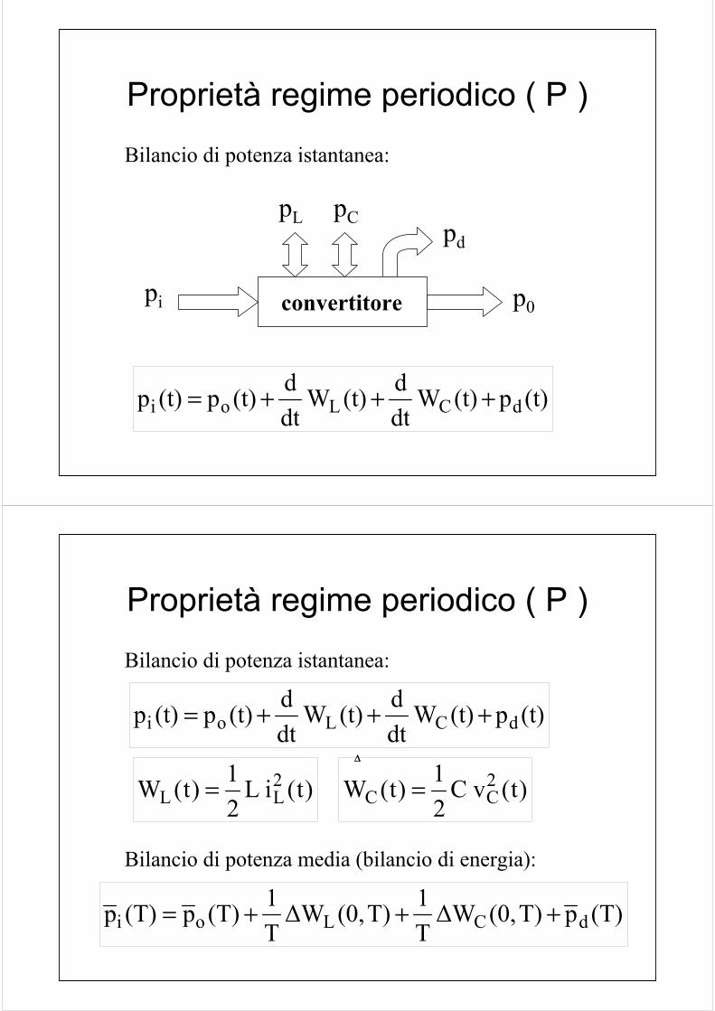
Proprietà regime periodico ( P )
(t)p(t)Wdtd(t)W
dtd(t)p(t)p dCLoi +++=
Bilancio di potenza istantanea:
p0pi
pLpd
pC
convertitore
Proprietà regime periodico ( P )
(t)p(t)Wdtd(t)W
dtd(t)p(t)p dCLoi +++=
Bilancio di potenza istantanea:
)t(iL21)t(W 2
LL = )t(vC21)t(W 2
CC =
Bilancio di potenza media (bilancio di energia):
(T)pT)(0,∆WT1T)(0,∆W
T1(T)p(T)p dCLoi +++=
∆∆
Proprietà regime periodico ( P )
In condizioni periodiche, a regime:
0)T,0(W )0(i)T(i LLL =∆⇒=
Bilancio di potenza media (bilancio di energia):
doi PPP +=
0)T,0(W )0(v)T(v CCC =∆⇒=
trascurando le perdite
Proprietà regime periodico ( P )
Calcolo delle potenze medie, attenzione!
)T(i)T(v dt)t(i)t(vT1 )T(p P
T
0
⋅≠⋅== ∫
Il valor medio del prodotto è in generale diverso dal prodotto dei valori medi, a meno che una o entrambe le grandezze siano costanti
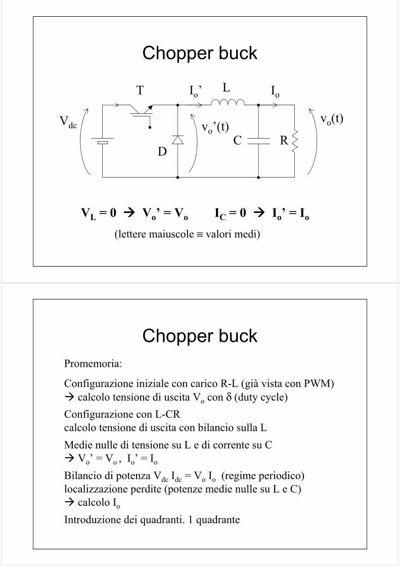
Chopper buck
L
C R
T
D
Vdcvo(t)
IoIo’
vo’(t)
VL = 0 Vo’ = Vo IC = 0 Io’ = Io
(lettere maiuscole ≡ valori medi)
Chopper buckPromemoria:
Configurazione iniziale con carico R-L (già vista con PWM)calcolo tensione di uscita Vo con δ (duty cycle)
Configurazione con L-CRcalcolo tensione di uscita con bilancio sulla LMedie nulle di tensione su L e di corrente su C
Vo’ = Vo , Io’ = Io
Bilancio di potenza Vdc Idc = Vo Io (regime periodico)localizzazione perdite (potenze medie nulle su L e C)
calcolo Io
Introduzione dei quadranti. 1 quadrante

Chopper boost
D
C R
L
Vdc
Vo
Io
T
Chopper boost
Promemoria:
Calcolo tensione di uscita con bilancio sulla L
Bilancio di potenza Vdc Idc = Vo Iocalcolo Io
Chopper abbassatore di corrente
1 quadrante

Chopper a ramo completo
V1
V2
Chopper a ramo completo
Promemoria:
2 quadranti
Da un lato abbassatore, dall’altro innalzatore
Recupero energia (motore o carico attivo)
Controllo completo tensione per Io > < 0
Introduzione dei “tempi morti”
Chopper buck-boostPer ottenere in uscita una tensione che può essere sia inferiore che superiore alla tensione di alimentazione si potrebbe pensare ad un collegamento in cascata di chopper tipo “buck” e tipo “boost” controllati con lo stesso duty-cycle δ:
( ) dcdco V1
V1
1Vδ−
δ=δδ−
=
In pratica vengono utilizzate configurazioni piùsemplici che realizzano lo stesso rapporto tra ingresso ed uscita ma con polarità invertita.
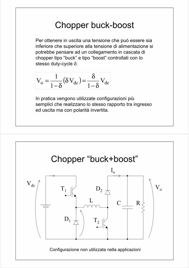
Chopper “buck+boost”
L C R
T1
D1
Vdc Vo
Io
T2
D2
Configurazione non utilizzata nella applicazioni
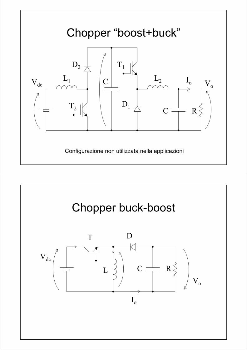
Chopper “boost+buck”
L1 C
T2
D2
Vdc
T1
D1
L2
C R
VoIo
Configurazione non utilizzata nella applicazioni
Chopper buck-boost
L C R
T D
Vdc
Vo
Io
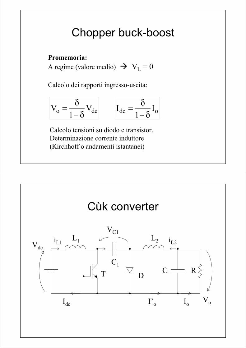
Chopper buck-boost
Promemoria:A regime (valore medio) VL = 0
Calcolo dei rapporti ingresso-uscita:
dco V1
Vδ−
δ= odc I1
Iδ−
δ=
Calcolo tensioni su diodo e transistor.Determinazione corrente induttore(Kirchhoff o andamenti istantanei)
Cùk converter
L1 L2
C1C RT D
Vdc
VoI’o
VC1iL1 iL2
IoIdc
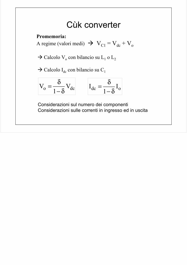
Cùk converterPromemoria:A regime (valori medi) VC1 = Vdc + Vo
Calcolo Vo con bilancio su L1 o L2
Calcolo Idc con bilancio su C1
dco V1
Vδ−
δ= odc I1
Iδ−
δ=
Considerazioni sul numero dei componentiConsiderazioni sulle correnti in ingresso ed in uscita
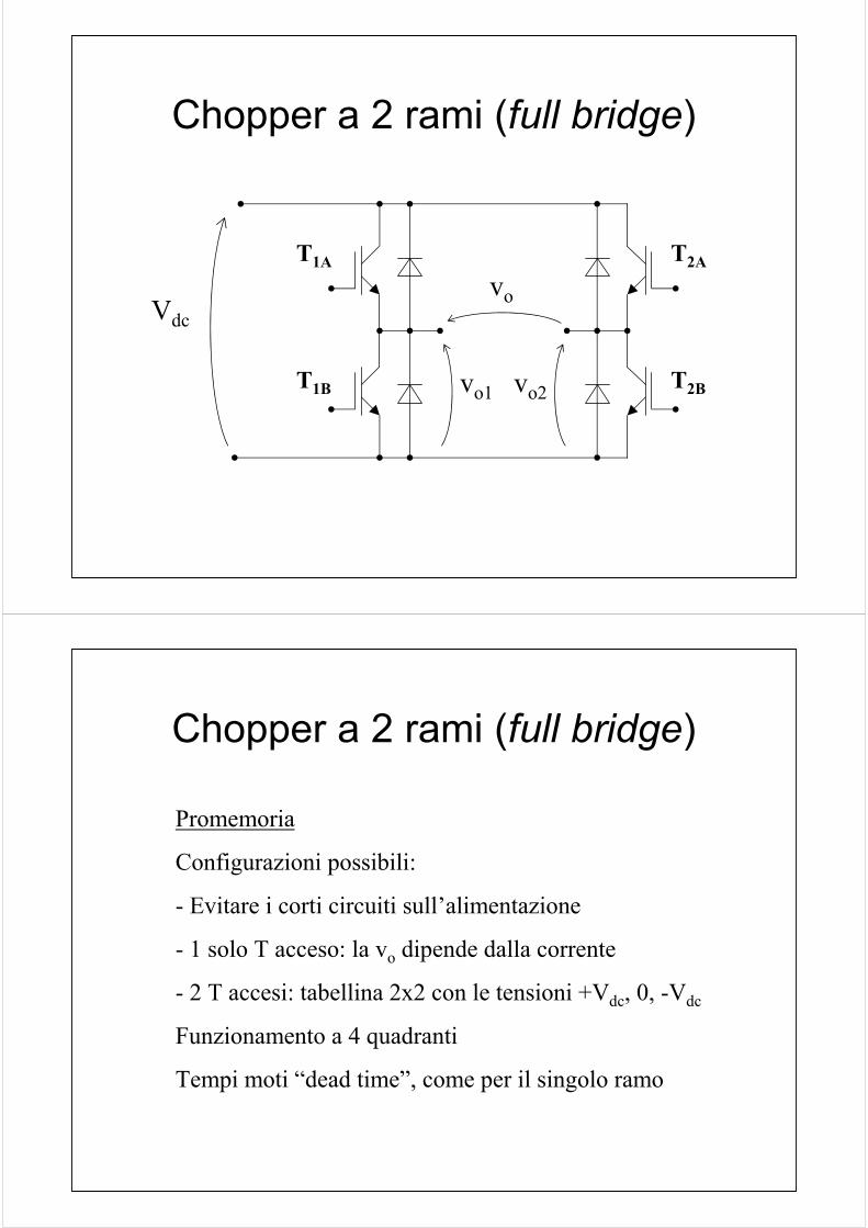
Chopper a 2 rami (full bridge)
Vdcvo
vo1 vo2
T1A
T1B
T2A
T2B
Chopper a 2 rami (full bridge)
Promemoria
Configurazioni possibili:
- Evitare i corti circuiti sull’alimentazione
- 1 solo T acceso: la vo dipende dalla corrente
- 2 T accesi: tabellina 2x2 con le tensioni +Vdc, 0, -Vdc
Funzionamento a 4 quadranti
Tempi moti “dead time”, come per il singolo ramo

Controllo bipolareControllo con vo che varia tra +Vdc e −Vdc
2 livelli possibili di tensione di uscita
dc
*o
11
V2v
21
Tt +=δ=
Si considerano le due configurazioni (diagonali):
T1A e T2B on +Vdc , ton = t1 , δ1
T2A e T1B on −Vdc , ton = t2 , δ2
dc
*o
22
V2v
21
Tt −=δ=
Ttt 21 =+
Controllo bipolare
0
Vdc
-Vdc
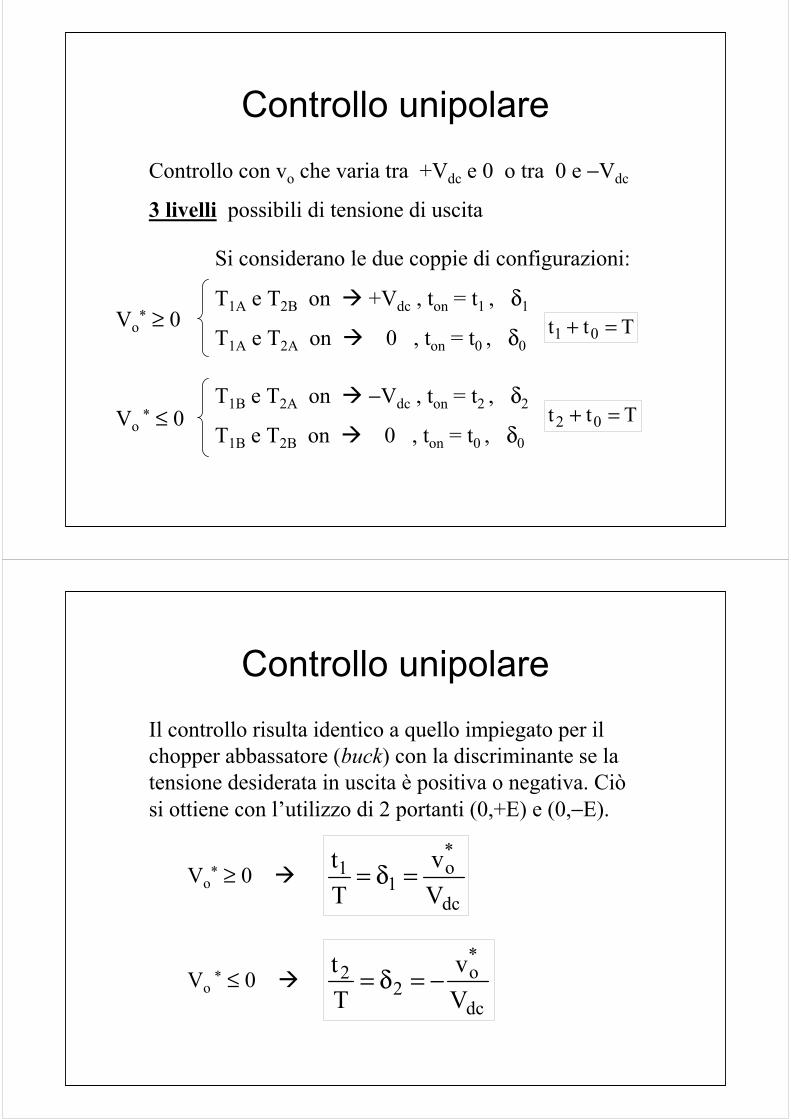
Controllo unipolareControllo con vo che varia tra +Vdc e 0 o tra 0 e −Vdc
3 livelli possibili di tensione di uscita
Si considerano le due coppie di configurazioni:
T1A e T2B on +Vdc , ton = t1 , δ1
T1A e T2A on 0 , ton = t0 , δ0
T1B e T2A on −Vdc , ton = t2 , δ2
T1B e T2B on 0 , ton = t0 , δ0
Ttt 01 =+
Ttt 02 =+
Vo* ≥ 0
Vo * ≤ 0
Controllo unipolareIl controllo risulta identico a quello impiegato per il chopper abbassatore (buck) con la discriminante se la tensione desiderata in uscita è positiva o negativa. Ciò si ottiene con l’utilizzo di 2 portanti (0,+E) e (0,−E).
dc
*o
11
Vv
Tt =δ=
dc
*o
22
Vv
Tt −=δ=
Vo* ≥ 0
Vo * ≤ 0

Controllo unipolare
ramo 1
ramo 2
0
Vdc
-Vdc
Controllo unipolareIn alternativa si può realizzare il controllo unipolarecontrollando separatamente i due rami, utilizzando la una sola portante e due modulanti, sfruttando la relazione:
2
*o*
o2 K2
vv +−=
1
*o*
1o K2
vv +=
2o1oo vvv −=
Per rispettare il vincolo 0 ≤ vo1, vo2 ≤ Vdc si assume:
K1 = K2 = Vdc /2
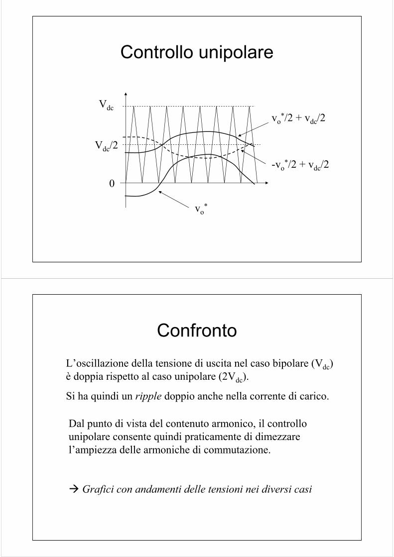
Controllo unipolare
Vdc/2
Vdc
0
vo*
vo*/2 + vdc/2
-vo*/2 + vdc/2
ConfrontoL’oscillazione della tensione di uscita nel caso bipolare (Vdc) è doppia rispetto al caso unipolare (2Vdc).
Si ha quindi un ripple doppio anche nella corrente di carico.
Dal punto di vista del contenuto armonico, il controllo unipolare consente quindi praticamente di dimezzare l’ampiezza delle armoniche di commutazione.
Grafici con andamenti delle tensioni nei diversi casi
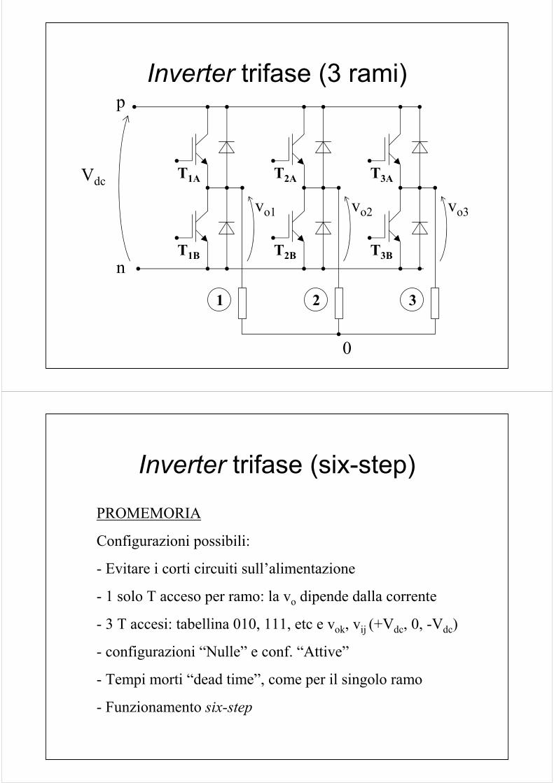
Inverter trifase (3 rami)
Vdc
vo1
T1A
T1B
vo2 vo3
T2A
T2B
T3A
T3B
1 2 3
0
p
n
Inverter trifase (six-step)
PROMEMORIA
Configurazioni possibili:
- Evitare i corti circuiti sull’alimentazione
- 1 solo T acceso per ramo: la vo dipende dalla corrente
- 3 T accesi: tabellina 010, 111, etc e vok, vij (+Vdc, 0, -Vdc)
- configurazioni “Nulle” e conf. “Attive”
- Tempi morti “dead time”, come per il singolo ramo
- Funzionamento six-step
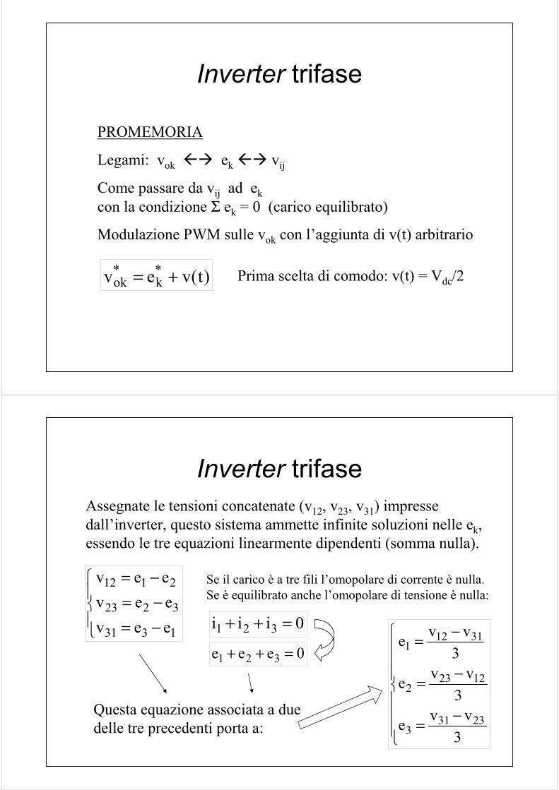
Inverter trifase
PROMEMORIA
Legami: vok ek vij
Come passare da vij ad ekcon la condizione Σ ek = 0 (carico equilibrato)
Modulazione PWM sulle vok con l’aggiunta di v(t) arbitrario
)t(vev *k
*ok += Prima scelta di comodo: v(t) = Vdc/2
Inverter trifaseAssegnate le tensioni concatenate (v12, v23, v31) impresse dall’inverter, questo sistema ammette infinite soluzioni nelle ek, essendo le tre equazioni linearmente dipendenti (somma nulla).
−=
−=
−=
3vve
3vve
3vve
23313
12232
31121
0iii 321 =++
0eee 321 =++
−=−=−=
1331
3223
2112
eeveeveev
Questa equazione associata a duedelle tre precedenti porta a:
Se il carico è a tre fili l’omopolare di corrente è nulla.Se è equilibrato anche l’omopolare di tensione è nulla:

Inverter trifase
TkA
TkB
k
ek
vn00
p
n
ek = vkn + vn0
e1 + e2 + e3 = 0 =
= v1n + v2n + v3n + 3 vn0
vn0 = − 1/3 (v1n+v2n+ v3n )
0 ≤ vkn ≤ Vdc vkn = ek* + c(t)
ek = ek* + c(t) − 1/3 (e1
*+e2*+ e3
* ) − c(t)
ek = ek* = 0
vkn
Inverter trifase
PROMEMORIA
Limite nella tensioni di uscita con v(t) = Vdc/2
Massimizzazione ampiezze di uscita variando v(t)
Considerazioni su perdite e rendimento(potenze attiva, reattiva ed apparente del carico)
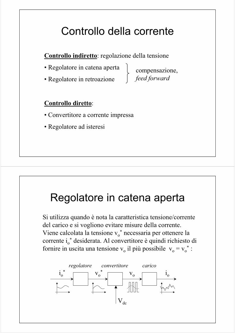
Controllo della corrente
Controllo indiretto: regolazione della tensione
• Regolatore in catena aperta
• Regolatore in retroazione
Controllo diretto:
• Convertitore a corrente impressa
• Regolatore ad isteresi
compensazione,feed forward
Regolatore in catena apertaSi utilizza quando è nota la caratteristica tensione/correntedel carico e si vogliono evitare misure della corrente.Viene calcolata la tensione vo
* necessaria per ottenere lacorrente io
* desiderata. Al convertitore è quindi richiesto difornire in uscita una tensione vo il più possibile vo = vo
* :
io* vo
* vo io
Vdc
caricoconvertitoreregolatore
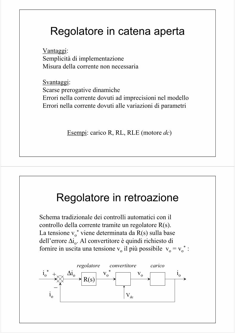
Regolatore in catena apertaVantaggi:Semplicità di implementazioneMisura della corrente non necessaria
Svantaggi:Scarse prerogative dinamicheErrori nella corrente dovuti ad imprecisioni nel modelloErrori nella corrente dovuti alle variazioni di parametri
Esempi: carico R, RL, RLE (motore dc)
Regolatore in retroazioneSchema tradizionale dei controlli automatici con ilcontrollo della corrente tramite un regolatore R(s).La tensione vo
* viene determinata da R(s) sulla base dell’errore ∆io. Al convertitore è quindi richiesto difornire in uscita una tensione vo il più possibile vo = vo
* :
io* vo
* vo io
Vdc
caricoconvertitoreregolatore
R(s)
io
+_
∆io
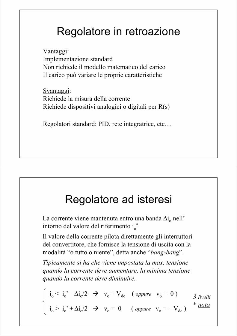
Regolatore in retroazioneVantaggi:Implementazione standardNon richiede il modello matematico del caricoIl carico può variare le proprie caratteristiche
Svantaggi:Richiede la misura della correnteRichiede dispositivi analogici o digitali per R(s)
Regolatori standard: PID, rete integratrice, etc…
Regolatore ad isteresiLa corrente viene mantenuta entro una banda ∆io nell’intorno del valore del riferimento io
*.
Il valore della corrente pilota direttamente gli interruttoridel convertitore, che fornisce la tensione di uscita con lamodalità “o tutto o niente”, detta anche “bang-bang”.Tipicamente si ha che viene impostata la max. tensionequando la corrente deve aumentare, la minima tensionequando la corrente deve diminuire.
io < io* − ∆io/2 vo = Vdc ( oppure vo = 0 )
io > io* + ∆io/2 vo = 0 ( oppure vo = −Vdc )
3 livelli* nota

Regolatore ad isteresi
io*
∆io
io*+ ∆io/2
io* − ∆io/2
Vdc
0
vo
Regolatore ad isteresiLa presenza della banda d’isteresi limita la frequenzadi commutazione che altrimenti sarebbe elevatissima.La frequenza di commutazione è funzione inversadell’ampiezza della banda e della costante di tempoL/R del carico.
Vantaggi:Semplicità di implementazione analogicaInsensibilità alla variazioni del caricoSvantaggi:Commutazioni non uniformi nel periodoFrequenza di commutazione variabile
Convertitori diretti ac/ac
Non hanno un bus dc intermedio
• Chopper ac
• Matrix converter
Interruttore bidirezionale
driver* nota
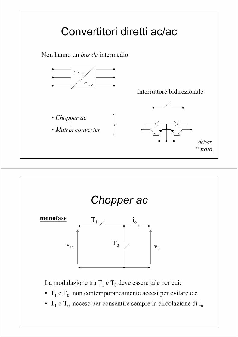
Chopper ac
vac vo
T1
T0
La modulazione tra T1 e T0 deve essere tale per cui:• T1 e T0 non contemporaneamente accesi per evitare c.c.• T1 o T0 acceso per consentire sempre la circolazione di io
iomonofase
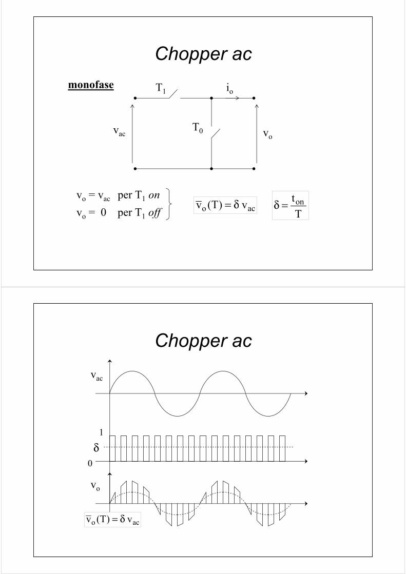
Chopper ac
vac vo
T1
T0
vo = vac per T1 onvo = 0 per T1 off
io
aco v)T(v δ=T
ton=δ
monofase
Chopper acvac
0
1
δ
vo
aco v)T(v δ=
Chopper ac
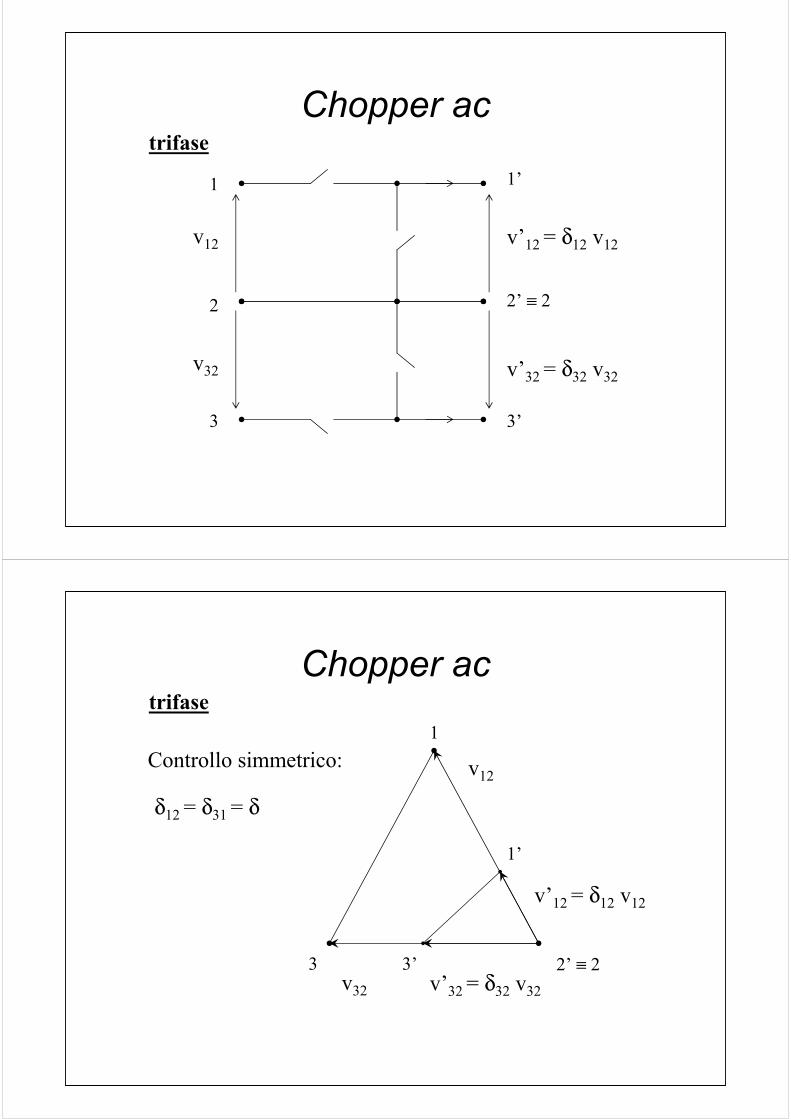
v12
v32
1
2
3
2’ ≡ 2
1’
3’
v’12 = δ12 v12
v’32 = δ32 v32
trifase
Chopper ac
1
3 2’ ≡ 2
1’
3’
v12
v32
v’12 = δ12 v12
v’32 = δ32 v32
Controllo simmetrico:
δ12 = δ31 = δ
trifase

Matrix converter
1
2
3
1’ 2’ 3’
Condizioni per i T sulle fasi di uscita:Non c.c. sull’alimentazione• Non più di un T accesoContinuità corrente di carico• Almeno un T acceso
9 interruttoribidirezionali
Limite in uscita: Vo ≤ 0.866 Vac
Vo
Vac

Perdite e rendimentoLa potenza mediamente dissipata da un interruttoreelettronico in un ciclo di lavoro Tc vale in generale:
)T(P)T(P)T(P ccommccondcd +=
commoocccomm t2IVkf)T(P ⋅=
ooc
condccond IvIv
Tt)T(P ⋅∆⋅δ=⋅∆=
Con riferimento alla struttura ad 1 ramo completo:
( 2 tcomm = ton + toff )
Perdite di conduzioneSi suppone in prima approssimazione che transistor e diodiabbiano le stesse cadute di tensione ∆v.
Vdc
vo
io
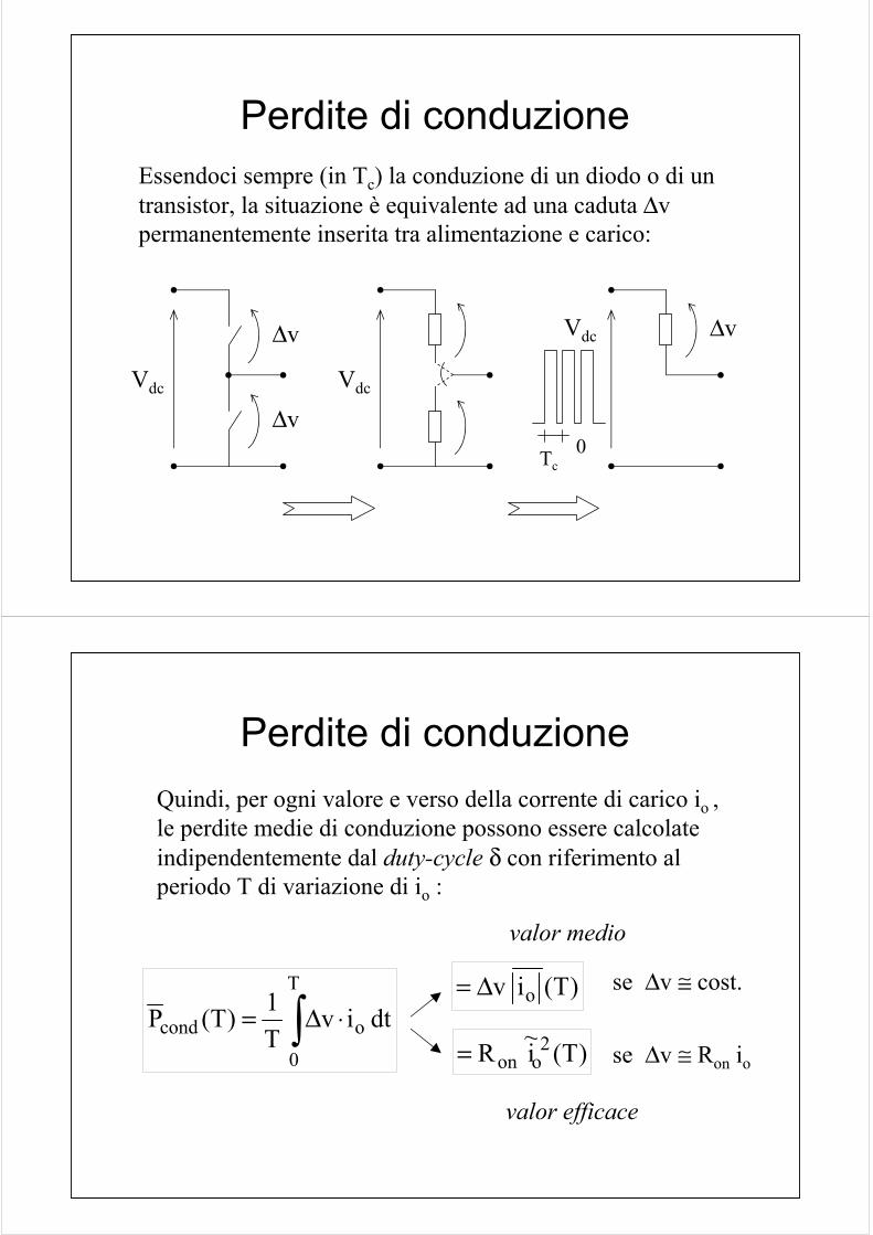
Perdite di conduzioneEssendoci sempre (in Tc) la conduzione di un diodo o di untransistor, la situazione è equivalente ad una caduta ∆vpermanentemente inserita tra alimentazione e carico:
Vdc Vdc
Vdc
0
∆v∆v
∆vTc
Perdite di conduzioneQuindi, per ogni valore e verso della corrente di carico io , le perdite medie di conduzione possono essere calcolateindipendentemente dal duty-cycle δ con riferimento alperiodo T di variazione di io :
∫ ⋅∆=T
0
ocond dtivT1)T(P
)T(iv o∆= se ∆v ≅ cost.
)T(i~R 2oon= se ∆v ≅ Ron io
valor medio
valor efficace
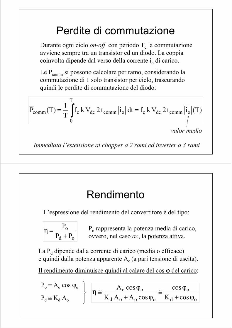
Perdite di commutazioneDurante ogni ciclo on-off con periodo Tc la commutazione avviene sempre tra un transistor ed un diodo. La coppia coinvolta dipende dal verso della corrente io di carico.
Le Pcomm si possono calcolare per ramo, considerando la commutazione di 1 solo transistor per ciclo, trascurandoquindi le perdite di commutazione del diodo:
Immediata l’estensione al chopper a 2 rami ed inverter a 3 rami
)T(it2Vkfdtit2VkfT1)T(P ocommdcc
T
0
ocommdcccomm == ∫valor medio
RendimentoL’espressione del rendimento del convertitore è del tipo:
od
oPP
P+
=η Po rappresenta la potenza media di carico, ovvero, nel caso ac, la potenza attiva.
La Pd dipende dalla corrente di carico (media o efficace)e quindi dalla potenza apparente Ao (a pari tensione di uscita).
Il rendimento diminuisce quindi al calare del cos ϕ del carico:
Po = Ao cos ϕo
Pd ≅ Kd Ao od
o
oood
oocosK
coscosAAK
cosAϕ+
ϕ≅ϕ+
ϕ≅η
Comportamento termicodei componenti
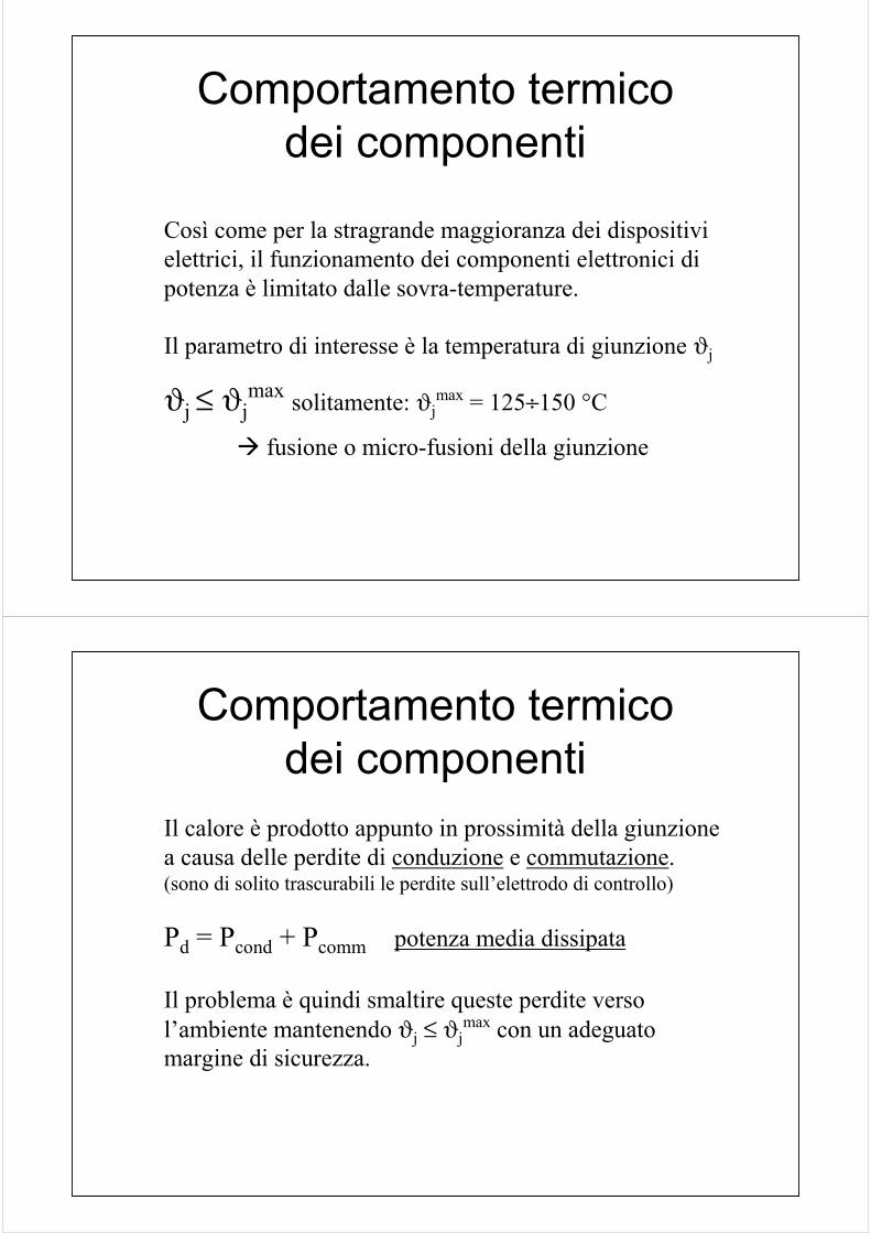
Il parametro di interesse è la temperatura di giunzione ϑj
ϑj ≤ ϑjmax solitamente: ϑj
max = 125÷150 °C
fusione o micro-fusioni della giunzione
Così come per la stragrande maggioranza dei dispositivi elettrici, il funzionamento dei componenti elettronici di potenza è limitato dalle sovra-temperature.
Il calore è prodotto appunto in prossimità della giunzione a causa delle perdite di conduzione e commutazione.(sono di solito trascurabili le perdite sull’elettrodo di controllo)
Pd = Pcond + Pcomm potenza media dissipata
Il problema è quindi smaltire queste perdite verso l’ambiente mantenendo ϑj ≤ ϑj
max con un adeguato margine di sicurezza.
Comportamento termicodei componenti
Le variabili di interesse sono quindi:
ϑj temperatura di giunzione
Pd potenza media dissipata
I parametri da considerare sono:
ϑa temperatura ambiente (costante)
ϑjmax temperatura max. giunzione
E’ possibile rappresentare il legame tra temperaturae potenza introducendo una rete termica.
Comportamento termicodei componenti
Struttura dei componenti
Vedi componenti reali e disegni alla lavagna
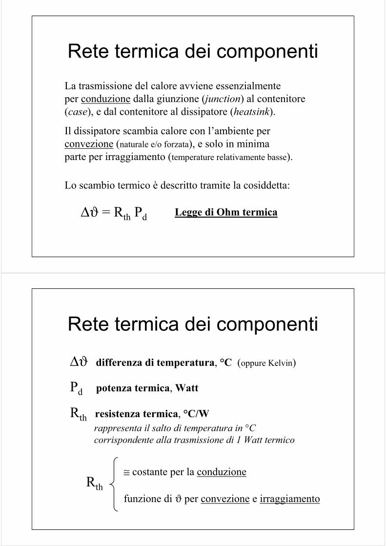
Rete termica dei componentiLa trasmissione del calore avviene essenzialmenteper conduzione dalla giunzione (junction) al contenitore (case), e dal contenitore al dissipatore (heatsink).
Il dissipatore scambia calore con l’ambiente per convezione (naturale e/o forzata), e solo in minimaparte per irraggiamento (temperature relativamente basse).
Lo scambio termico è descritto tramite la cosiddetta:
Legge di Ohm termica∆ϑ = Rth Pd
Rete termica dei componenti
∆ϑ differenza di temperatura, °C (oppure Kelvin)
Pd potenza termica, Watt
Rth resistenza termica, °C/Wrappresenta il salto di temperatura in °C corrispondente alla trasmissione di 1 Watt termico
Rth≅ costante per la conduzione
funzione di ϑ per convezione e irraggiamento
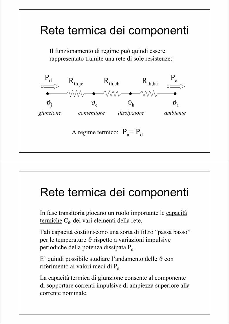
Rete termica dei componentiIl funzionamento di regime può quindi essere rappresentato tramite una rete di sole resistenze:
Rth,jc Rth,ch Rth,ha
giunzione
ϑj ϑc ϑh ϑa
contenitore dissipatore ambiente
Pd Pa
A regime termico: Pa= Pd
Rete termica dei componentiIn fase transitoria giocano un ruolo importante le capacitàtermiche Cth dei vari elementi della rete.
Tali capacità costituiscono una sorta di filtro “passa basso”per le temperature ϑ rispetto a variazioni impulsive periodiche della potenza dissipata Pd.
E’ quindi possibile studiare l’andamento delle ϑ con riferimento ai valori medi di Pd.
La capacità termica di giunzione consente al componente di sopportare correnti impulsive di ampiezza superiore alla corrente nominale.
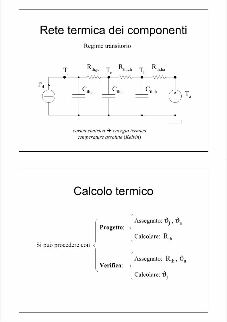
Rete termica dei componentiRegime transitorio
Rth,jc Rth,ch Rth,haTj Tc Th
Ta
Pd Cth,j Cth,c Cth,h
carica elettrica energia termicatemperature assolute (Kelvin)
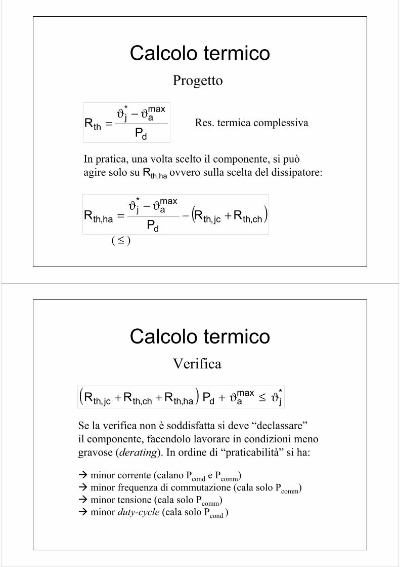
Calcolo termico
Si può procedere con
Progetto:
Verifica:
Assegnato: ϑj , ϑa
Calcolare: Rth
Assegnato: Rth , ϑa
Calcolare: ϑj
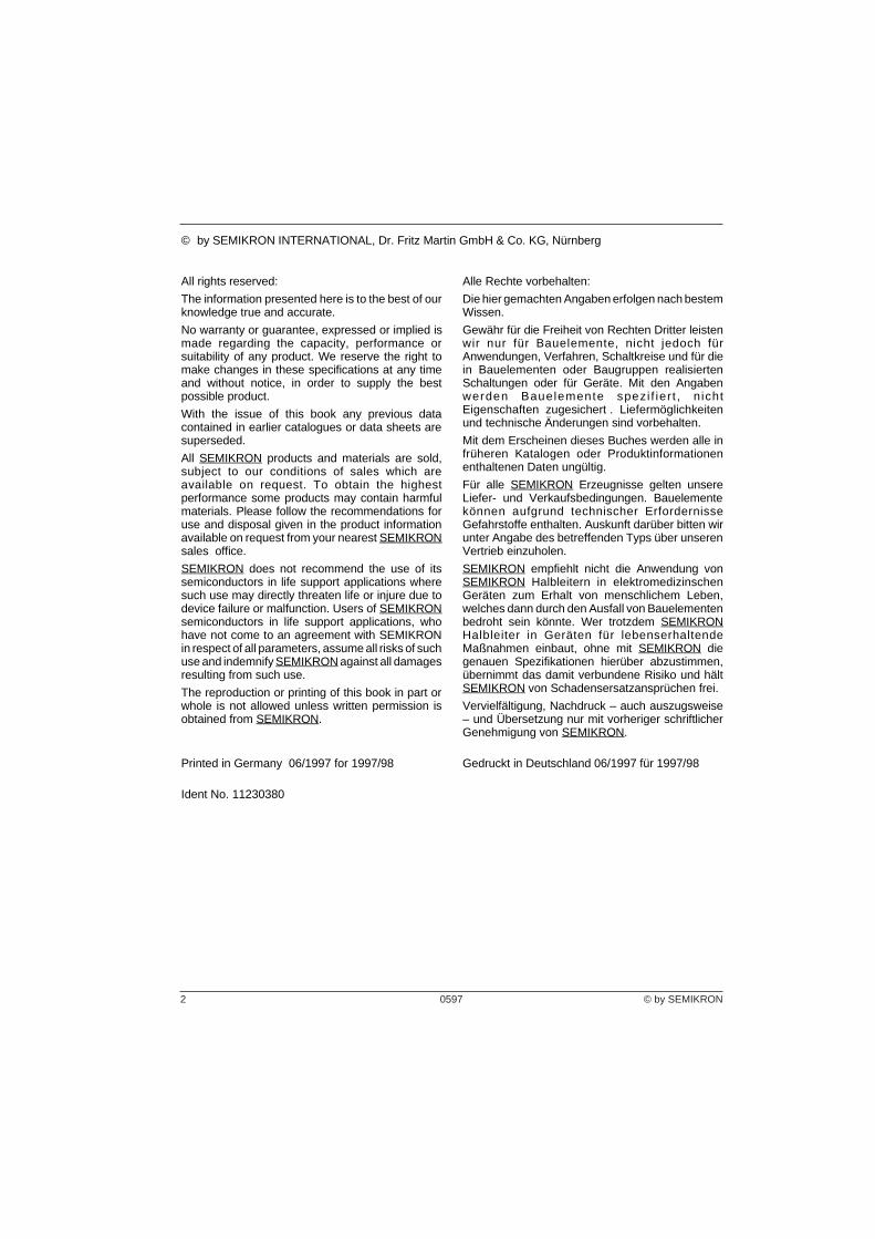
Calcolo termicoProgetto
d
maxa
*j
th PR
ϑ−ϑ=
In pratica, una volta scelto il componente, si può agire solo su Rth,ha ovvero sulla scelta del dissipatore:
( )ch,thjc,thd
maxa
*j
ha,th RRP
R +−ϑ−ϑ
=
Res. termica complessiva
( ≤ )
Calcolo termicoVerifica
Se la verifica non è soddisfatta si deve “declassare”il componente, facendolo lavorare in condizioni meno gravose (derating). In ordine di “praticabilità” si ha:
( ) *j
maxadha,thch,thjc,th PRRR ϑ≤ϑ+++
minor corrente (calano Pcond e Pcomm)minor frequenza di commutazione (cala solo Pcomm)minor tensione (cala solo Pcomm)minor duty-cycle (cala solo Pcond )

Leistungselektronik
Power Electronics
SEMIKRON INTERNATIONAL Dr. Fr i tz Mart in GmbH & Co. KGSigmundstr. 200, D-90431 Nürnberg / GermanyPostfach 82 02 51, D-90253 Nürnberg / GermanyTelefon (09 11) 65 59-0 +49.911.6559.0Telefax (09 11) 65 59-262 +49.911.6559.262Telex 622 155 semi de-mail: [email protected] (→ C-36)
© by SEMIKRON2
All rights reserved:
The information presented here is to the best of ourknowledge true and accurate.
No warranty or guarantee, expressed or implied ismade regarding the capacity, performance orsuitability of any product. We reserve the right tomake changes in these specifications at any timeand without notice, in order to supply the bestpossible product.
With the issue of this book any previous datacontained in earlier catalogues or data sheets aresuperseded.
All SEMIKRON products and materials are sold,subject to our conditions of sales which areavailable on request. To obtain the highestperformance some products may contain harmfulmaterials. Please follow the recommendations foruse and disposal given in the product informationavailable on request from your nearest SEMIKRONsales office.
SEMIKRON does not recommend the use of itssemiconductors in life support applications wheresuch use may directly threaten life or injure due todevice failure or malfunction. Users of SEMIKRONsemiconductors in life support applications, whohave not come to an agreement with SEMIKRONin respect of all parameters, assume all risks of suchuse and indemnify SEMIKRON against all damagesresulting from such use.
The reproduction or printing of this book in part orwhole is not allowed unless written permission isobtained from SEMIKRON.
Printed in Germany 06/1997 for 1997/98
Ident No. 11230380
Alle Rechte vorbehalten:
Die hier gemachten Angaben erfolgen nach bestemWissen.
Gewähr für die Freiheit von Rechten Dritter leistenwir nur für Bauelemente, nicht jedoch fürAnwendungen, Verfahren, Schaltkreise und für diein Bauelementen oder Baugruppen realisiertenSchaltungen oder für Geräte. Mit den Angabenwerden Bauelemente spezi f ier t , n ichtEigenschaften zugesichert . Liefermöglichkeitenund technische Änderungen sind vorbehalten.
Mit dem Erscheinen dieses Buches werden alle infrüheren Katalogen oder Produktinformationenenthaltenen Daten ungültig.
Für alle SEMIKRON Erzeugnisse gelten unsereLiefer- und Verkaufsbedingungen. Bauelementekönnen aufgrund technischer ErfordernisseGefahrstoffe enthalten. Auskunft darüber bitten wirunter Angabe des betreffenden Typs über unserenVertrieb einzuholen.
SEMIKRON empfiehlt nicht die Anwendung vonSEMIKRON Halbleitern in elektromedizinschenGeräten zum Erhalt von menschlichem Leben,welches dann durch den Ausfall von Bauelementenbedroht sein könnte. Wer trotzdem SEMIKRONHalbleiter in Geräten für lebenserhaltendeMaßnahmen einbaut, ohne mit SEMIKRON diegenauen Spezifikationen hierüber abzustimmen,übernimmt das damit verbundene Risiko und hältSEMIKRON von Schadensersatzansprüchen frei.
Vervielfältigung, Nachdruck – auch auszugsweise– und Übersetzung nur mit vorheriger schriftlicherGenehmigung von SEMIKRON.
Gedruckt in Deutschland 06/1997 für 1997/98
© by SEMIKRON INTERNATIONAL, Dr. Fritz Martin GmbH & Co. KG, Nürnberg
0597

a Maximum acceleration under vibration
b Width of the module base
B2 Two-pulse bridge connection
B6 Six-pulse bridge connection
CCHC Capacitance chip-case (baseplate)
Cies Input capacitance, output short-circuited
Ciss Input capacitance, output short-circuited
Cj Junction capacitance
Cmax Maximum value of reservoir capacitor (forgreater values of capacitance the recommend-ed current must be reduced)
cont Continuous direct current
Coss Output capacitance (input shorted)
Cps Coupling capacitance between the primary win-ding and each secondary winding
Crss Reverse transfer capacitance(Miller capacitance)
D Duty cycle. D = f . tp
∅ D Contact diameter of capsule devices
(di/dt)cr Critical rate of rise of on-state current
– diD/dt Rate of fall of the drain current (MOSFET)
– diF/dt Rate of fall of the forward current (diode)
diG/dt Rate of rise of gate current
– diT/dt Rate of fall of the on-state current (thyr.)
diT/dt Rate of rise of on-state current (thyr.)
(dv/dt)cr Critical rate of rise of off-state voltage
DSC Double sided cooling
Econd Energy dissipation duringt conduction time
ED Intermittend duty
e.m.f. Electromotoric force (back e.m.f.) = generatedvoltage of a rotating machine
Eoff Energy dissipation during turn-off time
Eon Energy dissipation during turn-on time
Err Energy dissipation during reverse recovery (diode)
f Operating frequency, pulse frequency
fG Maximum frequency
F Mounting force
Fu Recommended fuse (fast acting)
gfs Forward transconductance
IAOmax Max. output current (driver)
IC Continuous collector current
ICES Collector-emitter cut-off current withgate-emitter short-circuited
ICETRIP Max. ICE to trip ERROR (SKiiP)
ICM Peak collector current
ICp Non-repetitive peak collector current
ICsat Collector current for VCEsat test
ICRM Repetitive peak collector current
Id Direct output current (of a rectifier connection)
ID (Direct) off-state current (thyristors)
ID Maximum direct output current of the completecircuit (bridge circuits)
ID Continuous drain current (MOSFETs)
IDC Continuous direct current (diode)
IDCL Direct output current with capacitive load(limiting value)
IDD Direct off-state current
IDM Peak value of a pulsed drain current
IDR Continuous reverse drain current(inverse diode forward current)
IDRM Pulsed reverse drain current, peak value(pulsed inverse diode forward current)
IDSS Zero gate voltage drain current (gate shorted)
IE Continuous emitter current
iF Forward current (instantaneous value)
IF Forward current
IF(OV) Overload forward current
IFAV Mean forward current
IFAV(B) Mean basic load current
IFCL Mean forward current with capacitive load
IFM Peak forward current
IFN Recommended mean forward current
IFRM Repetitive peak forward current
IFRMS RMS forward current
IFSM Surge forward current
IFWM Peak forward working current
IG Gate current
IGD Gate non-trigger current
IGES Gate-emitter leakage current, collector-emittershort-circuited
IGoff Output current (peak) max. for switch-off(driver
IGon Output current (peak) max. for switch-on (driver)
IGSS Gate-source leakage current, drain-sourceshort-circuited
IGT Gate trigger current
IH Holding current
IiH Input signal current (HiGH)
IL Latching current
Letter Symbols and Terms
0996© by SEMIKRON A – 1

0996 © by SEMIKRONA – 2
IM Highest peak current obtainable at a rise timelower than 1 µs (pulse transformers)
IN Recommended direct output current withresistive load
INCL Recommended direct output current with ca-pacitive load
INRMS Nominal r.m.s. current (of a fuse)
IoutAV Output average current (driver)
IR Reverse current
IR0 Reverse current for calculating the reverse po-wer dissipation
IRD Direct reverse current
IRM Peak reverse recovery current
Irms Alternating output current(of an a.c. controller connection)
IRMS Maximum rated r.m.s. current of a completea.c. controller connection
irr Reverse recovery current(measuring condition for tf and trr)
IRRM Peak reverse recovery current
IRSM Maximum permissible non-repetitive peak re-verse current (avalanche diodes)
IS Supply current primary side
ISO Supply current primary side (driver) at no load
iT On-state current (instantaneous value)
IT (Direct) on-state current
ITAV Mean on-state current
ITM Peak on-state current
IT(OV) Overload on-state current
ITRMS RMS on-state current
ITSM Surge on-state current
i2t i2t value
Î Peak pulse current(IEC standard pulse 8 x 20 µs)
IZ Tail current (IGBT)
K Factor from the relation Zthjc:Rthjc
L External collector inductance
I Length of the heatsink profile
LCE Parasitic collector-emitter inductance
LDS Parasitic drain-source inductance
Lp Inductance of the primary winding at 1 kHz
Lss Parasitic inductance (sec. stray inductance)
M Mounting torque
M1 Torque for mounting the semiconductor to theheatsink
M2 Torque for mounting the busbars to the semi-conductor
Mac Mounting torque for AC terminals
Mdc Mounting torque for DC terminals
n Number of semiconductor components(modules) on a common heatsink
n Number of load cycles
N Maximum number of series connected siliconelements
Np/Ns Ratio of windings primary to secondary
∆p Pressure drop
P Power dissipation of one component
PAV Maximum permissible permanent power dissi-pation average value
PD Power dissipation
PFAV Mean forward power dissipation
PFM Peak forward power dissipation
PG Peak gate power dissipation
PR Reverse power dissipation
PRAV Mean reverse power dissipation (thyr.)
PRRM Peak repetitive reverse power dissipation
PRSM Non-repetitive peak reverse power dissipation
PTAV Mean on-state power dissipation (thyristor)
PTOT
PVTOTTotal power dissipation
pw Water pressure
Qf Charge recovered during the reverse currentfall time
Qgel Gate charge (IGBT)
Qgsl Gate-source charge (MOSFET)
Qrr Recovered charge
R Number of rows of heatsinks one on top of theother
RC Recommended snubber network
RCE Resistor for VCE monitoring
RDS(on) Drain-source on-resistance (MOSFET)
rec ... Rectangular current waveform
rec. 120 Rectangular pulses, 120° conduction angle
REX Auxiliary emitter series resistor (parallel IGBT)
RG Gate circuit resistance
RGoff External gate series resistor at switch-off(MOSFET, IGBT)
RGon External gate series resistor at switch-on(MOSFET, IGBT)
RGS Gate-source resistance (MOSFET)
^
Letter Symbols and Terms

0996© by SEMIKRON A – 3
RL Load resistance for measuring tr and IM(pulse transformer)
Rmin Recommended series resistor for capacitiveloads (source resistance included in this value)
Rp Recommended parallel resistor for use with se-ries connection
Rp D.C. resistance of the primary winding
rpm Revolutions per minute
Rs D.C. resistance of each secondary winding
rT On-state slope resistance, forward sloperesistance
RTD Resistor for interlock dead time (driver)
Rthca Thermal resistance case to ambient air
Rthch Contact thermal resistance case to heatsink1)
Rthcw Thermal resistance case to cooling water
Rthha Thermal resistance heatsink to ambient air
Rthja Thermal resistance junction to ambient air
Rthjc Thermal resistance junction to case
R(thjc)p Thermal resistance junction to case under pul-se conditions
Rthjr Thermal resistance junction to reference point
Rthjoil Thermal resistance junction to oil
Rthjw Thermal resistance junction to cooling water
Rthmw Thermal resistance thermal trip-cooling water
sin... Sinusoidal current waveform
sin. 180 Half sinewaves, 180° conduction angle
SSC Single sided cooling
t Time
Tamb Ambient temperature
Tbtt Switching temperature of the attached bimetalthermal trip
tc Period (cycle) duration
Tcase Case temperature
tcond Conducting time
td Delay time
td(err) ERROR input-output propagation delay time(driver)
td(off) Turn-off delay time
td(off)io Input-output turn-off propagation delay time(driver)
td(on) Turn-on delay time
td(on)io Input-output turn-on propagation delay time(driver)
Terr Max. temperature for setting ERROR
te On-time
tf Reverse current fall time (diode)
tf Fall time
tfr Forward recovery time
tgd Gate controlled delay time
Th Heatsink temperature
tif current fall time
tir current rise time
Tj Junction temperature
Toil Oil temperature (at the hottest place) duringoperating in insulating oil
toff Turn-off time
ton Turn-on time
Top Operating temperature range
tp Pulse duration
tpdon-err Propagation delay time on ERROR
tpRESET Min. pulse width ERROR memory RESET time
tq Circuit commutated turn-off time (thyristor)
tr Rise time
tR Reverse blocking time: tR = tc – tp
Tref Reference point temperature
trr Reverse recovery time
tsp Cycle time
Tstg Storage temperature range
Ttp Over temperature protection (SKiiP)
Tvj Virtual junction temperature
Tw Water temperature
tZ Tail time (IGBT)
∫ vdt Voltage-time integral at no load
vair Air velocity
Vair Air volume
Vair/t Air flow
V(BR) Avalanche breakdown voltage
V(BR)CES Collector-emitter breakdown voltage,gate-emitter short circuited
V(BR)DSS Drain-source breakdown voltage,gate-source short circuited
VCC Collector-emitter supply voltage
VCE Collector-emitter (direct) voltage
VCEclamp Collector-emitter clamping voltage during turn-off
VCES Collector-emitter (direct) voltage with base-(gate-)emitter short-circuited
VCEsat Collector-emitter saturation voltage1) Note: see page A – 7, Note 1
Letter Symbols and Terms

0996 © by SEMIKRONA – 4
VCEstat Collector-emitter threshold static monitoringvoltage
VCEdyn Collector-emitter threshold dynamic monito-ring voltage
Vcond Drain-source (collector-emitter-)voltage in theconducting state
VD Direct output voltage (bridge rectifier)
VD (Direct) off-state voltage (thyristor)
VDD Direct off-state voltage (thyristor)
VDD Drain-source supply voltage (MOSFET)
VDGR Drain-gate voltage with specified input resist-ance
VDRM Repetitive peak off-stage voltage
VDS Drain-source voltage
VEE Emitter supply voltage
vF Forward voltage (instantaneous value)
VF (Direct) forward voltage
VG Gate voltage
VGD Gate non-trigger voltage
VGE Gate-emitter voltage
VGES Gate-emitter voltage, collector-emittershort-circuited
VGE(th) Gate-emitter threshold voltage
VG(off) Turn-off gate voltage output
VG(on) Turn-on gate voltage output
VGS Gate-source voltage
VGS(th) Gate-source threshold voltage
VGT Gate trigger voltage
ViH Input signal voltage (HIGH) max.
VISOL Insulation test voltage (r.m.s.)
VisolIO Isolation test voltage (r.m.s. / 1 min.)input-outpt (driver)
Visol12 Isolation test voltage (r.m.s. / 1 min.) output1 - output 2 (driver)
ViT+ Input threshold voltage (HIGH) min.
ViT– Input threshold voltage (LOW) max.
Volw Water volume per unit time
VoH Logic HIGH output voltage (driver)
VoL Logic LOW output voltage (driver)
Vp Peak pulse voltage
VR (Direct) reverse voltage
VRD Direct reverse voltage
VRGM Peak reverse gate voltage
VRGO No-load reverse gate voltage
VRRM Repetitive peak reverse voltage
VRSM Non-repetitive peak reverse voltage
VRWM Crest working reverse voltage
VS Supply voltage primary (for gate driver)
VS1 Supply voltage stabilized
VS2 Supply voltage non stabilized
VSD Negative source-drain voltage(inverse diode forward voltage)
vT On-state voltage (instantaneous value)
VT (Direct) on-state voltage (thyr.)
V(TO)
VT(TO)Threshold voltage
VUSV Supply undervoltage monitoring
Vv Alternating line voltage (r.m.s.)
VVRMS Alternating input voltage (r.m.s. value)
Vw Water volume
VWW Maximum alternating working voltage betweenwindings (r.m.s. value) (pulse transformer)
w Weight
W1 Single phase a.c. controller connection
W3 Three phase a.c. controller connection
Wcond Energy dissipation during the conducting time
WF, EF Forward energy dissipation
Woff, Eoff Energy dissipation during the turn-off time
Won,Eon Energy dissipation during the turn-on time
Wp, Ep Maximum permissible non-repetitive peak pul-se energy (rectangular pulse 2 ms)
Zth Transient thermal impedance
Zthca Transient thermal impedance case to ambient
Zthjc Transient thermal impedance junction to case
ZthjcD Transient thermal impedance junction to caseof the freewheeling diode (brake chopperIGBT module)
Zthjh Transient thermal impedance junction to heat-sink
Zthha Transient thermal impedance heatsink to am-bient air
Z(th)p Transient thermal impedance under pulse con-ditions
Z(th)t Transient thermal impedance
Z(th)z Supplementary transient thermal impedance
Θ Conduction angle
Letter Symbols and Terms

0996© by SEMIKRON A – 5
CurrentsIrmsAlternating output current (of an a.c. controller
connection)
ICsatCollector current for VCEsat test
ICESCollector-emitter cut-off current withbase-(gate-)emitter short-circuited
IcontContinuous direct current
ICContinuous collector current
IDContinuous direct drain current (MOSFETs)
IDCContinuous direct current (diode)
IEContinuous emitter current
IDRContinuous reverse drain current (inversediode forward current)
IF(Direct) forward current (diode)
ID, IDD(Direct) off-state current (thyristor)
IT(Direct) on-state current (thyristor)
IdDirect output current (of a rectifier connection)
IDCLDirect output current with capacitive load
IRDDirect reverse current
IFGForward gate (trigger) current
iFForward current (instantaneous value)
IGGate current
IGDGate non-trigger current
IGSSGate-source leakage current (output shorted)
IGTGate trigger current
IMHighest peak current obtainable at a rise timelower than 1 µs (pulse transformer)
IHHolding current
IiHInput signal current (High)
ILLatching current
ICETRIPMaximum collector current to trip ERROR(SkiiP)
IdMaximum direct output current
IGDMaximum gate non-trigger current
IAOMaximum output current (driver)
IDMaximum output direct current of the completecircuit (bridge circuits)
IGonMaximum peak output current (of driver) forswitch-on (IGBT)
IGoff Maximum peak output current (of driver) forswitch-off (IGBT)
IRSMMaximum permissible non-repetitive peakreverse current
IRMSMaximum r.m.s. current of a complete a.c.controller connectionIRSM
IFAV(B)Mean basic load current
IFAVMean forward current
IFCLMean forward current with capacitive load
ITAVMean on-state current
INRMSNominal r.m.s. current
INRMSNominal r.m.s. current of a fuse
ICpNon-repetitive peak collector current
iTOn-state current (instantaneous value)
IoutAVOutput average current (driver)
IF(OV)Overload forward current
IT(OV)Overload on-state current
ICMPeak collector current
IFMPeak forward current
IFWMPeak forward working current
ITMPeak on-state current
ÎPeak pulse current(IEC standard pulse 8 ×20 µs)
IRM, IRRMPeak reverse recovery current
IDMPeak value of a pulsed drain current
IF(OV)Permissible overload current
IDRMPulsed reverse drain current (pulsed inversediode forward current)
INRecommended direct output current withresistive load
INCLRecommended direct output current withcapacitive load
IFNRecommended mean forward current
ICRMRepetitive peak collector current
IFRMRepetitive peak forward current
IRReverse current
irrReverse recovery current(measuring condition for tf and trr)
IFRMSRMS forward current
ITRMSRMS on-state current
ISSupply current primary side (driver)
ISOSupply current primary side (driver) at no load
IFSMSurge forward current (diode)
ITSMSurge on-state current (thyristor)
IZTail current (IGBT)
IDSSZero gate voltage drain current (gate shorted)
VoltagesVVAlternating line voltage (r.m.s.)
VVRMSAlternating input voltage (r.m.s.)
Terms and Letter Symbols

0996 © by SEMIKRONA – 6
V(BR)Avalanche break-down voltage
VCEclampCollector-emitter clamping voltageduring turn-off
VCECollector-emitter (direct) voltage
VCESCollector-emitter (direct) voltage withgate-emitter short-circuited
VCEstatCollector-emitter-monitoring threshold voltage (static) (driver)
VCEsatCollector-emitter saturation voltage
VCCCollector-emitter supply voltage
VFContinuous forward voltage
VCCEContinuous collector emitter voltage
VcondContinuous conduction voltage
VRWMCrest working reverse voltage
VD, VDDDirect off-state voltage (thyristor)
VT(Direct) on-state voltage
VDDirect output voltage (bridge rectifier)
VRD, VRDirect reverse voltage
VDGRDrain-gate voltage with specified inputresistance
V(BR)DSSDrain-source breakdown voltage(input short circuited)
VDDDrain-source supply voltage
VDSDrain-source voltage
VcondDrain-source (collector-emitter) voltage in theconducting state
VCEdynDynamic collector-emitter-monitoringthreshold voltage (driver)
VEEEmitter supply voltage
VDPForward spike voltage
vFForward voltage (instantaneous value)
VGGate voltage
VGS(th)Gate-source threshold voltage
VGSGate-source voltage
VGTGate trigger voltage
ViHInput signal voltage (HIGH) max.
ViT+Input threshold voltage (HIGH) min.
ViT-Input threshold voltage (LOW) max.
VISOLInsulation test voltage (r.m.s.) betweenprimary and secondary windings (pulsetransformer)
VISOLInsulation test voltage (r.m.s.)
VisolIOInsulation test voltage (rms, 1 min)input-output (driver)
Visol12Insulation test voltage rms, 1 min.output 1 - output 2 (driver)
VOHLogic HIGH output voltage (driver)
VOLLogic LOW output voltage (driver)
VWWMaximum alternating working voltage betweenwindings (r.m.s. value) (pulse transformer)
VGDMaximum gate non-trigger voltage
VSDNegative source-drain voltage (inverse diodeforward voltage)
VRGONo-load reverse gate voltage
VRSMNon-repetitive peak reverse voltage
vTOn-state voltage (instantaneous value) (thyr)
VpPeak pulse voltage
VRGMPeak reverse gate voltage
VDRMRepetitive peak off-stage voltage
VRRMRepetitive peak reverse voltage
VCEstatStatic Collector-emitter-monitoring threshold voltage (static) (driver)
VUSVSupply undervoltage monitoring
VS2Supply voltage non stabilized
VSSupply voltage primary (for driver)
VS1Supply voltage stabilized
V(TO)Threshold voltage (rectifier diode)
VT(TO)Threshold voltage (thyristor)
VG(off)Turn-off gate voltage
VG(on)Turn-on gate voltage output
Rates of fall, rates of rise(dv/dt)crCritical rate of rise of off-state voltage
(di/dt)crCritical rate of rise of on-state current
– diD/dtRate of fall of the drain current (MOSFET)
– diF/dtRate of fall of the forward current (diode)
– diT/dtRate of fall of the on-state current (thyr.)
diG/dtRate of rise of the gate current
diT/dtRate of rise of the on-state current (thyr.)
Power dissipations, energy dissipationsEcondEnergy dissipation during the conducting time
ErrEnergy dissipation during the reverse recoverytime (fast driver)
EoffEnergy dissipation during the turn-off time
EonEnergy dissipation during the turn-on time
EpMaximum permissible non-repetitive peakpulse energy (rectangular pulse 2 ms)
PAVMaximum permissible permanent powerdissipation
PFAVMean forward power dissipation
PTAVMean on-state power dissipation
PRAVMean reverse power dissipation
PRSMNon-repetitive peak reverse power dissipation
^
^
Terms and Letter Symbols

0996© by SEMIKRON A – 7
PGPeak gate power dissipation
PRRMPeak repetitive reverse power dissipation
PDPower dissipation
PPower dissipation of one component
PRReverse power dissipation
PTOT, PVTOTTotal power dissipation
CapacitancesCCHCCapacitance chip-case (baseplate)
CpsCoupling capacitance between the primarywinding and each secondary winding
CiesInput capacitance (output shorted) (IGBT)
CissInput capacitance (output shorted) (MOSFET)
CjJunction capacitance
CmaxMaximum value of reservoir capacitor
CresReverse transfer capacitance (Millercapacitance) IGBT
Crss MOSFET
CoesOutput capacitance (input shorted) IGBT
Coss MOSFET
InductancesLExternal collector inductance
LpInductance of the primary winding at 1 kHz
LssParasitic inductance
LDSParasitic drain-source inductance (MOSFET)
LCEParasitic collector-emitter inductance (IGBT)
ResistancesREXAuxiliary emitter resistor (parall. IGBT)
RpD.C. resistance of the primary winding
RsD.C. resistance of each secondary winding
RDS(on)Drain-source on-resistance
RGEExternal resistance between gate and emitter
rTForward slope resistance
RGGate circuit resistance
RGoffGate series resistor at switch-off
RGonGate series resistor at switch-on
RGSGate-source resistance
RLLoad resistance for measuring tr and IMrTOn-state slope resistance
RpRecommended parallel resistorfor use with series connection
RminRecommended series resistor forcapacitive loads (source resistanceincluded in this value)
Thermal ResistancesRthchContact thermal resistance case to heatsink 1)
RthcaThermal resistance case to ambient air
RthcwThermal resistance case to cooling water
RthhaThermal resistance heatsink to ambient air
RthjaThermal resistance junction to ambient air
RthjcThermal resistance junction to case
R(thjc)pThermal resistance junction to case underpulse conditions
RthjwThermal resistance junction to cooling water
Rthj oilThermal resistance junction to oil
RthjrThermal resistance junction to reference point
RthmwThermal resistance thermal trip-cooling water
Transient thermal impedancesZ(th)zSupplementary transient thermal impedance
Zth, Z(th)tTransient thermal impedance
ZthcaTransient thermal impedance case to ambientair
ZthhaTransient thermal impedance heatsink toambient air
ZthjcTransient thermal impedance junction to case
ZthjhTransient thermal impedance junction toheatsink
Z(th)pTransient thermal impedance under pulseconditions
Z(th)pDTransient thermal impedance under pulseconditions of the diode (IGBT-modules)
TimestqCircuit commutated turn-off time (thyristor)
tcondConducting time
teConduction time (welding) (SKN 4000, SKIW..)
tcCycle time
tsCycle time (welding)
tifCurrent fall time
tirCurrent rise time
tdDelay time
tfFall time
tfgForward gate (trigger) current pulse duration
tfrForward recovery time
tgdGate controlled delay time
tgrGate controlled rise time
tspLoad cycle time (SKN 4000, SKIW..)
^
1) Note: Test point and measurement of heatsink temp. Th of all SEMIKRON modules see page A – 52, 3rd paragr.
Terms and Letter Symbols
0996 © by SEMIKRONA – 8
tcPeriod (cycle) duration (SKN 4000, SKIW..)
tpPulse duration
tRReverse blocking time: tR = tc–tp
tfReverse current fall time
trrReverse recovery time
trRise time
tsSin wave period duration (welding)
tzTail time (IGBT)
tTime
td(off)Turn-off delay time
toffTurn-off time
td(on)Turn-on delay time
tonTurn-on time
TemperaturesTambAmbient temperature
TcaseCase temperature
ThHeatsink temperature 1)
TjJunction temperature
ToilOil temperature (at the hottest place) duringoperating in insulating oil
TrefReference point temperature
TstgStorage temperature range
TbitSwitching temperature of the attached bimetalthermal trip
TvjVirtual junction temperature
TwWater temperature
Various TermsVair/tAir flow
vairAir velocity
VairAir volume
QfCharge recovered during the reverse currentfall time
ΘConduction angle
∅DContact diameter of capsule devices
DSCDouble sided cooling
DDuty cycle D=f . tpe.m.f.Electromotoric forces (back e.m.f) = generated
voltage of a rotating machine
KFactor from the relation Zthjc:Rthjc
gfsForward transconductance (MOSFET, IGBT)
QG, QgelGate turn-off charge (IGBT)
QgslGate-source charge (MOSFET)
sin. 180Half sinewaves, 180° conduction angle
i2ti2t value
ILength of the heatsink profile
aMaximum acceleration under vibration
fGMaximum frequency
NMaximum number of series connected siliconelements
FMounting force
MMounting torque
RNumber of rows of heatsinks one on top of theother
nNumber of semiconductor components(modules) on a common heatsink
fOperating frequency, pulse frequency
∆pPressure drop
Np/NsRatio of windings
FuRecommended fuse (fast acting)
RCRecommended snubber network
QrrRecovered charge
rec. 120Rectangular pulses, 120° conduction angle
rec...Rectangular current waveform
EDRelative overload duration, intermittend duty
rpmRevolutions per minute
sin.Sinusoidal current waveform
sin. 180Sinusoidal pulses, 180° conduction angle
W1Single phase a.c. controller connection
SSCSingle sided cooling
B6Six-pulse bridge connection
W3Three phase a.c. controller connection
MTorque for assembly
M1Torque for mounting the semiconductor to theheatsink
M2Torque for mounting the busbars to thesemiconductor
B2Two-pulse bridge connection
∫ vdtVoltage-time integral at no load
PwWater pressure
VwWater volume
VolwWater volume per unit time
wWeight
bWidth of the module base
WWidth of the heatsink (P 21)
1) see Note 1) page A – 7
Terms and Letter Symbols

© by SEMIKRON B 8 – 10597
Section 8: Rectifier Diodes
Summary of Types
Type VRRM IFRMS IFAV @Tcase IFSM i2t Case PageVRSM sin. 10 ms 10 ms
180 25 °C 25 °C
V A A °C A A2s
SK 1 1 000 ... 1 600 3 1,15 451) 60 18 E 33B 8-5
SK 3 1 000 ... 1 600 6,7 1,8 451) 180 162 E 34
SKN 2,5 400 ... 1 600 5 2,5 451) 180 160 E 5B 8-9
SKN 5 200 ... 1 600 10 5 451) 190 180 E 6
SKN 20 200 ... 1 600 40 20 125 375 700 E 9SKR 20B 8-13
SKN 26 200 ... 1 600 40 20 125 375 700 E 8SKR 26
SKN 45 200 ... 1 600 80 45 125 700 2 500 E 12SKR 45
SKN 70 200 ... 1 600 150 70 125 1 150 6 600 E 12 B 8-17SKR 70
SKN 71 200 ... 1 600 150 70 125 1 150 6 600 E 11SKR 71
SKN 100 200 ... 1 800 200 100 125 1 750 15 000 E 13SKR 100
SKN 130 200 ... 1 800 260 130 125 2 500 31 000 E 14 B 8-21SKR 130
SKN 240 200 ... 1 800 500 240 125 6 000 180 000 E 15SKR 240
SKN 320 200 ... 1 600 700 320 125 9 000 400 000 E 16SKR 320 B 8-25
SKN 400 1 800 ... 3 000 700 400 100 9 000 400 000 E 17
SKN 450 1 800 ... 2 200 450 95 6 000 180 000 E 18
SKN 501 400 ... 1 800 500 125 7 000 245 000 E 18 B 8-29
SKN 870 400 ... 2 400 870 105 13 000 850 000 E 19
SKN 1500 400 ... 2 900 1 500 78 19 000 1,8 . 106 E 20
SKN 2000 600 ... 2 400 2 000 75 30 000 4,5 . 106 E 21B 8-33
SKN 3000 2 200 ... 3 600 3 100 75 38 500 7,4 . 106 E 37
SKN 3400 1 200 ... 1 800 3 425 75 51 500 13,25 . 106 E 37B 8-37
SKN 4000 200 ... 600 6 300 4 000 50 60 000 18 . 106 E 22
SKN 6000 200 ... 600 10 000 6 000 85 60 000 18 . 106 E 35B 8-41
1) Tamb
SKN SKR(Anode to stud) (Cathode to stud)
continued next page

© by SEMIKRON B 8 – 21
Rectifier Diodes
SKN 100 SKR 100SKN 130 SKR 130SKN 240 SKR 240
Features• Reverse voltages up to 1600 V• Hermetic metal cases with
glass insulators• Threaded studs ISO M 12,
M16 x 1,5 (SKR 130 also 1/2–20 UNF or 3/8–24 UNF, SKR 240 also 3/4–16 UNF)
• SKN: anode to studSKR: cathode to stud
Typical Applications• All-purpose mean power
rectifier diodes• Cooling via heatsinks• Non-controllable and
half-controllable rectifiers• Free-wheeling diodes
♦ available in limited quantities* available with UNF threads:
3/8–24 UNF 2 A (e.g. SKR130/02UNF 3/8) or 1/2–20 UNF 2 A (e.g. SKR 130/02 UNF), SKR 240/02 UNF with 3/4–16 UNF 2 A thread
VRSM IFRMS (maximum values for continuous operation)VRRM 200 A 260 A 500 A
IFAV (sin. 180; Tcase = 100 °C)125 A 165 A 320 A
V
SKN SKR SKN SKR SKN SKR 200 100/02 100/02 130/02 130/02* 240/02 240/02* 400 100/04 100/04 130/04 130/04* 240/04 240/04* 800 100/08 100/08 130/08 130/08* 240/08 240/08*1200 100/12 100/12 130/12 130/12* 240/12 240/12*1400 100/14 100/14 130/14 130/14* 240/14 240/14*1600 100/16 100/16 130/16 130/16* 240/16 240/16*1800 100/18♦ 100/18♦ 130/18♦ 130/18♦ 240/18♦ 240/18♦
Symbol Conditions SKN 100 SKN 130 SKN 240SKR 100 SKR 130 SKR 240
IFAV sin. 180; Tcase = 100 °C 125 A 165 A 320 A
= 125 °C 100 A 130 A 240 A
IFSM Tvj = 25 °C; 10 ms 1 750 A 2 500 A 6 000 ATvj = 180 °C; 10 ms 1 500 A 2 000 A 5 000 A
i2t Tvj = 25 °C 8,3... 15 000 A2s 31 000 A2s 180 000 A2sTvj = 180 °C 10 ms 11 500 A2s 20 000 A2s 125 000 A2s
Qrr Tvj = 160 °C;
– diFdt
= 10 Aµs
typ. 100 µC typ. 120 µC typ. 200 µC
IR Tvj = 25 °C;VR = VRRM 1 mA 1 mA 2 mATvj = 180 °C;VR = VRRM 15 mA 22 mA 60 mA
VF Tvj = 25 °C;(IF = ...); max. 1,55V (400A) 1,5V (500A) 1,4V (750A)
V(TO) Tvj = 180 °C 0,85 V 0,85 V 0,85 V
rT Tvj = 180 °C 1,8 mΩ 1,3 mΩ 0,6 mΩ
Rthjc 0,45 °C/W 0,35 °C/W 0,20 °C/W
Rthch 0,08 °C/W 0,08 °C/W 0,03 °C/W
Tvj – 40 ... + 180 °CTstg – 55 ... + 180 °C
M SI units/US units 10Nm/90lb.in. 10Nm/90lb.in. 30Nm/270lb.in.
a 5 . 9,81 m/s2 5 . 9,81 m/s2 5 . 9,81 m/s2
w approx. 100 g 100 g 250 g
RC PR = 2 W 0,25µF + 50Ω 0,25µF + 50Ω 0,5µF + 30ΩRp PR = 20 W 50 kΩ 50 kΩ 50 kΩ
Case E 13 E 14 E 15
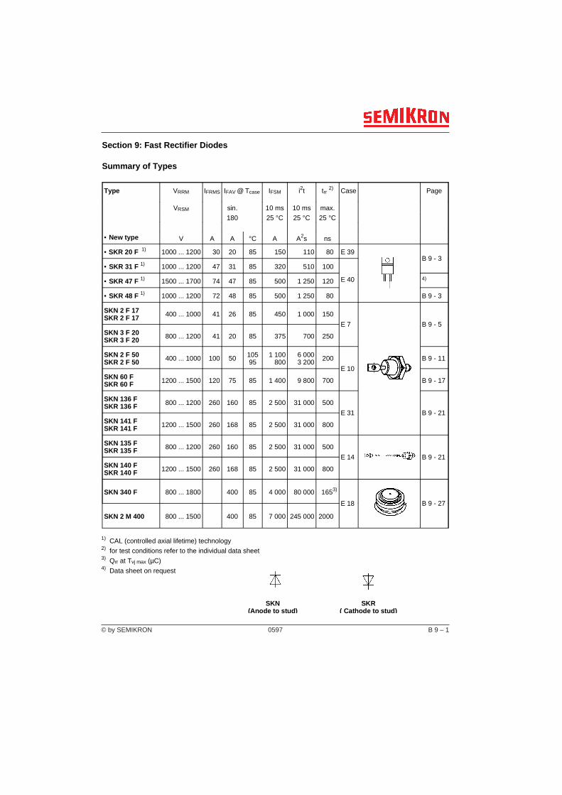
© by SEMIKRON B 9 – 10597
1) CAL (controlled axial lifetime) technology2) for test conditions refer to the individual data sheet3) Qrr at Tvj max (µC)4) Data sheet on request
SKN SKR(Anode to stud ) ( Cathode to stud )
Section 9: Fast Rectifier Diodes
Summary of Types
Type VRRM IFRMS IFAV @ Tcase IFSM i2t trr 2) Case Page
VRSM sin. 10 ms 10 ms max.
180 25 °C 25 °C 25 °C
• New type V A A °C A A2s ns
• SKR 20 F 1) 1000 ... 1200 30 20 85 150 110 80 E 39B 9 - 3
• SKR 31 F 1) 1000 ... 1200 47 31 85 320 510 100
E 40• SKR 47 F 1) 1500 ... 1700 74 47 85 500 1 250 120 4)
• SKR 48 F 1) 1000 ... 1200 72 48 85 500 1 250 80 B 9 - 3
SKN 2 F 17SKR 2 F 17 400 ... 1000 41 26 85 450 1 000 150
E 7 B 9 - 5SKN 3 F 20SKR 3 F 20 800 ... 1200 41 20 85 375 700 250
SKN 2 F 50SKR 2 F 50 400 ... 1000 100 50 105
951 100
8006 0003 200 200
E 10
B 9 - 11
SKN 60 FSKR 60 F 1200 ... 1500 120 75 85 1 400 9 800 700 B 9 - 17
SKN 136 FSKR 136 F 800 ... 1200 260 160 85 2 500 31 000 500
E 31 B 9 - 21SKN 141 FSKR 141 F 1200 ... 1500 260 168 85 2 500 31 000 800
SKN 135 FSKR 135 F 800 ... 1200 260 160 85 2 500 31 000 500
E 14 B 9 - 21SKN 140 FSKR 140 F 1200 ... 1500 260 168 85 2 500 31 000 800
SKN 340 F 800 ... 1800 400 85 4 000 80 000 1653)
E 18 B 9 - 27
SKN 2 M 400 800 ... 1500 400 85 7 000 245 000 2000

© by SEMIKRON B 9 – 17
Fast Recovery RectifierDiodes
SKN 60 F SKR 60 F
Features• Small recovered charge• Soft recovery• Up to 1500 V reverse voltage• Hermetic metal cases with
glass insulators• Threaded studs ISO M6 and M8• SKN: anode to stud
SKR: cathode to stud
Typical Applications• Inverse diodes for power
transistors, GTO thyristors,asymmetric thyristors
• SMPS, inverters, choppers• A. C. motor control,
uninterruptible power supplies(UPS)
VRSM IFRMS (maximum values for continuous operation)VRRM 120 A
IFAV (sin. 180; Tcase = 85 °C) 75 A
trr = 700 ns
V
1200 SKN 60 F 12 SKR 60 F 12
1400 SKN 60 F 14 SKR 60 F 14
1500 SKN 60 F 15 SKR 60 F 15
Symbol Conditions SKN 60 F UnitsSKR 60 F
IFAV sin. 180; Tcase =100 °C; f = 1000 Hz 60 A
sin.180/rec.120; Tamb = 45 °C; K5 15 / 14,5 AK3 21,5 / 21 A
K1,1 38 / 36,5 A
IFSM Tvj = 25 °C; 10 ms 1400 A
Tvj = 150 °C; 10 ms 1200 A
i2t Tvj = 25 °C; 8,3 ... 10 ms 9800 A2s
Tvj = 150 °C; 8,3 ... 10 ms 7200 A2s
Qrr Tvj = 150 °C; IF = 100 A; 75 µC
IRM – diF
dt = 100
Aµs
; VR = 30 V 70 A
IR Tvj = 25 °C; VR = VRRM 0,4 mA
Tvj = 150 °C; VR = VRRM 60 mA
trr Tvj = 25 °C max. 0,7 µs IF = IR = 1 ATvj = 150 °C typ. 1,4 µs
VF Tvj = 25 °C; IF = 150 A max. 1,75 V
V(TO) Tvj = 150 °C 1,0 V
rT Tvj = 150 °C 4 mΩ
Rthjc 0,5 °C/W
Rthch 0,25 °C/W
Tvj – 40 . . . + 150 °CTstg – 55 . . . + 150 °C
M SI units 2,5 Nm
US units 22 lb.in.
a 5 . 9,81 m/s2
w 20 g
Case E10

© by SEMIKRON B 3 – 1
Section 3: Thyristors
Summary of Types
Types VDRM ITRMS ITAV @ Tcase ITSM Tvj Rthjc Case PageVRRM
25 °C max. sin. 18010 ms
V A A °C A °C °C/W
SKT 10 600 . . . 1200 30 10 106 250 130 1,3
SKT 16 400 . . . 1600 40 16 103 370 130 0,9 B 3 - 7
SKT 24 400 . . . 1600 50 24 94 450 130 0,9
SKT 40 400 . . . 1800 63 38 85 700 130 0,66B 3 - 13
SKT 50 600 . . . 1800 78 45 85 1 050 130 0,60
SKT 55 400 . . . 1800 110 55 92 1 300 130 0,47
SKT 80 600 . . . 1800 135 80 85 1 700 130 0,28 B 3 - 17
SKT 100 400 . . . 1800 175 100 85 2 000 130 0,28
SKT 130 400 . . . 1600 220 130 85 3 500 130 0,18B 3 - 23
SKT 160 400 . . . 1600 280 160 85 4 300 130 0,18
SKT 250 400 . . . 1600 450 250 85 7 000 130 0,123 B 3 - 27
SKT 300 400 . . . 1600 550 350 85 11 000 130 0,096
SKT 240 400 . . . 2200 600 240 92 5 000 125 0,072
SKT 340 400 . . . 1800 700 340 82 5 700 125 0,072B 3 - 33
SKT 491 400 . . . 2200 1000 490 80 8 000 125 0,047B 3 - 37
SKT 551 800 . . . 1800 1200 550 85 9 000 125 0,047
SKT 520 1800 . . . 2800 1400 520 85 9 000 125 0,040 B 3 - 41
SKT 600 400 . . . 1800 1400 600 85 11 500 125 0,040B 3 - 45
SKT 760 400 . . . 1800 1600 760 80 15 000 125 0,040
SKT 1000 400 . . . 2800 2300 1000 85 19 000 125 0,0225B 3 - 49
SKT 1200 400 . . . 1800 2800 1200 85 30 000 125 0,0225
SKT 1400 2600 . . . 3600 3000 1400 62 29 000 125 0,0185 B 3 - 55
SKT 1800 1200 . . . 1600 4500 1800 85 53 000 125 0,0155 B 3 - 61
SKT 2000 2200 . . . 2800 5000 2000 72 45 000 125 0,0110 B 3 - 55
SKT 2400 1200 . . . 1800 5700 2400 75 55 000 125 0,0110 B 3 - 61
0895
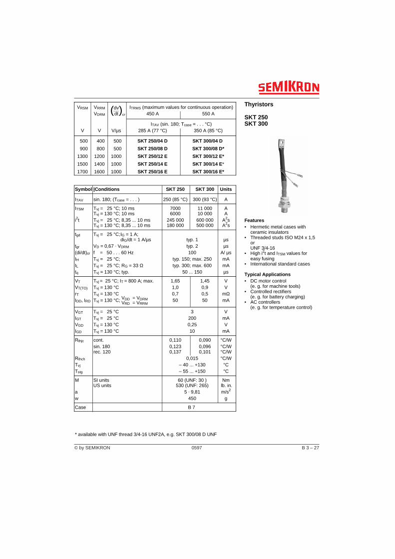
© by SEMIKRON B 3 – 27
Thyristors
SKT 250SKT 300
Features• Hermetic metal cases with
ceramic insulators• Threaded studs ISO M24 x 1,5
orUNF 3/4-16
• High i2t and ITSM values foreasy fusing
• International standard cases
Typical Applications• DC motor control
(e. g. for machine tools)• Controlled rectifiers
(e. g. for battery charging)• AC controllers
(e. g. for temperature control)
VRSM VRRM (dv) ITRMS (maximum values for continuous operation)VDRM dt cr 450 A 550 A
ITAV (sin. 180; Tcase = . . . °C)V V V/µs 285 A (77 °C) 350 A (85 °C)
500 400 500 SKT 250/04 D SKT 300/04 D
900 800 500 SKT 250/08 D SKT 300/08 D*
1300 1200 1000 SKT 250/12 E SKT 300/12 E*
1500 1400 1000 SKT 250/14 E SKT 300/14 E*
1700 1600 1000 SKT 250/16 E SKT 300/16 E*
Symbol |Conditions SKT 250 SKT 300 Units
ITAV sin. 180; (Tcase = . . . ) 250 (85 °C) 300 (93 °C) A
ITSM Tvj = 25 °C; 10 ms 7000 11 000 ATvj = 130 °C; 10 ms 6000 10 000 A
i2t Tvj = 25 °C; 8,35 ... 10 ms 245 000 600 000 A2sTvj = 130 °C; 8,35 ... 10 ms 180 000 500 000 A2s
tgd Tvj = 25 °C;IG = 1 A;diG/dt = 1 A/µs typ. 1 µs
tgr VD = 0,67 . VDRM typ. 2 µs(di/dt)cr f = 50 . . . 60 Hz 100 A/ µsIH Tvj = 25 °C; typ. 150; max. 250 mAIL Tvj = 25 °C; RG = 33 Ω typ. 300; max. 600 mAtq Tvj = 130 °C; typ. 50 ... 150 µs
VT Tvj = 25 °C; IT = 800 A; max. 1,65 1,45 VVT(TO) Tvj = 130 °C 1,0 0,9 VrT Tvj = 130 °C 0,7 0,5 mΩIDD, IRD Tvj = 130 °C; VDD = VDRM 50 50 mA VRD = VRRM
VGT Tvj = 25 °C 3 VIGT Tvj = 25 °C 200 mAVGD Tvj = 130 °C 0,25 VIGD Tvj = 130 °C 10 mA
Rthjc cont. 0,110 0,090 °C/Wsin. 180 0,123 0,096 °C/Wrec. 120 0,137 0,101 °C/W
Rthch 0,015 °C/WTvj – 40 ... +130 °CTstg – 55 ... +150 °C
M SI units 60 (UNF: 30 ) NmUS units 530 (UNF: 265) lb. in.
a 5 . 9,81 m/s2
w 450 g
Case B 7
* available with UNF thread 3/4-16 UNF2A, e.g. SKT 300/08 D UNF
0597
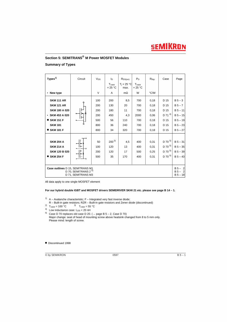
© by SEMIKRON B 5 – 1
Types 1) Circuit VDS ID RDS(on) PD Rthjc Case Page
Tcase Tj = 25 °C Tcase
= 25 °C max. = 25 °C
• New type V A mΩ W °C/W
SKM 111 AR 100 200 8,5 700 0,18 D 15 B 5 – 3
SKM 121 AR 200 130 20 700 0,18 D 15 B 5 – 7
SKM 180 A 020 200 180 11 700 0,18 D 15 B 5 – 11
• SKM 453 A 020 200 450 4,3 2000 0,06 D 71 4) B 5 – 15
SKM 151 F 500 56 110 700 0,18 D 15 B 5 – 19
SKM 181 800 36 240 700 0,18 D 15 B 5 – 23
SKM 181 F 800 34 320 700 0,18 D 15 B 5 – 27
SKM 204 A 50 200 3) 4,5 400 0,31 D 70 5) B 5 – 31
SKM 214 A 100 120 13 400 0,31 D 70 5) B 5 – 35
SKM 120 B 020 200 120 17 500 0,25 D 70 5) B 5 – 39
SKM 254 F 500 35 170 400 0,31 D 70 5) B 5 – 43
Case outlines D 15, SEMITRANS M1 B 5 – 2D 70, SEMITRANS 2 5) B 5 – 2D 71, SEMITRANS M3 B 5 – 18
Section 5: SEMITRANS ® M Power MOSFET Modules
Summary of Types
All data apply to one single MOSFET element
For our hybrid double IGBT and MOSFET drivers SEMIDRIVER SKHI 21 etc. please see page B 14 – 1.
1) A – Avalanche characteristic; F – Integrated very fast inverse diode; R – Built-in gate resistors; RZR – Built-in gate resistors and Zener diode (discontinued)2) Tcase = 100 °C 3) Tcase = 55 °C4) Low inductance case: LDS < 20 nH5) Case D 70 replaces old case D 20. (→ page B 5 – 2, Case D 70)
Major change: seat of head of mounting screw above heatsink changed from 8 to 5 mm only.Please mind: length of screw.
Discontinued 1998
0597

© by SEMIKRON B 5 – 39
SEMITRANS® MPower MOSFET Modules120 A, 200 V, 17 mΩ
SKM 120 B 020
Replaces discontinued SKM 224 A
Features
• N Channel, enhancement mode• Short internal connections
avoid oscillations• Switching kWs in less than 1 µs• Isolated copper baseplate using
Al2O3 ceramic Direct CopperBonding Technology (DCB)
• All electrical connections on topfor easy busbaring
• Large clearances and creepagedistances
• Material, clearances and cree-page distances meet UL-specifi-cations
Typical Applications
• Switched mode power supplies• DC servo and robot drives• DC choppers• UPS equipment• Plasma cutting• Not suitable for linear
amplification
This is an electrostatic dischar-ge sensitive device (ESDS).Please observe the internationalstandard IEC 747-1, Chapter IX.
Absolute Maximum RatingsSymbol Conditions 1) Values Units
VDS 200 VVDGR RGS = 20 kΩ 200 VID Tcase = 25 °C 120 A
Tcase = 85 °C 87 AIDM 360 AVGS ± 20 VPD 500 WTj, Tstg – 55 . . .+150 °CVisol AC, 1 min 2 500 Vhumidity DIN 40 040 Class Fclimate DIN IEC 68 T.1 55/150/56
Inverse DiodeIF= – ID 120 AIFM= – IDM 360 A
CharacteristicsSymbol Conditions 1) min. typ. max. Units
V(BR)DSS VGS = 0, ID = 0,25 mA 200 – – VVGS(th) VGS = VDS, ID = 1 mA 2,1 3,0 4,0 VIDSS VGS = 0 Tj = 25 °C – 50 250 µA
VGS = 200 V Tj = 125 °C – 300 1000 µAIGSS VGS = 20 V, VDS = 0 – 10 100 nARDS(on) VGS = 10 V, ID = 120 A – 15 17 mΩgfs VDS = 5 V, ID = 75 A 60 90 – S
CCHC per MOSFET – – 100 pFCiss VGS = 0 – 10,4 16 nFCoss VDS = 25 V – 2 4,5 nFCrss f = 1 MHz – 1 1,4 nFLDS – – 30 nH
td(on) VDD = 100 V – 120 – nstr ID = 75 A – 60 – nstd(off) VGS = 10 V – 240 – nstf RGS = 3,3 Ω – 40 – ns
Inverse DiodeVSD IF = 240 A, VGS = 0 – 1,2 1,5 Vtrr Tj = 25 °C 2) – 400 – ns
Tj = 150 °C 2) – 700 – nsQrr Tj = 25 °C 2) – 5,0 – µC
Tj = 150 °C 2) – 8 –
Thermal CharacteristicsRthjc per MOSFET – – 0,25 °C/WRthch per module – – 0,05 °C/W
Mechanical DataM1 to heatsink SI Units (M6) 4 – 5 Nm
US Units 35 – 44 lb.in.M2 for terminals SI Units (M5) 2,5 – 3,5 Nm
US Units 22 – 24 lb.in.a – – 5x9,81 m/s2
w – – 250 g
Case → page B 5 – 42 D 70
1) Tcase = 25 °C, unless otherwise specified.2) IF = – ID, VR = 100 V, – diF/dt = 100 A/µs
SEMITRANS 2
0896

© by SEMIKRON B 6 – 10796

© by SEMIKRON B 6 – 170996
SEMITRANS® MIGBT Modules
SKM 50 GB 123 DSKM 50 GAL 123 D
GB GAL
Features• MOS input (voltage controlled)• N channel, Homogeneous Si• Low inductance case• Very low tail current with low
temperature dependence• High short circuit capability,
self limiting to 6 * Icnom
• Latch-up free• Fast & soft inverse CAL
diodes8)
• Isolated copper baseplateusing DCB Direct Copper Bon-ding Technology
• Large clearance (10 mm) andcreepage distances (20 mm).
Typical Applications: → B 6 - 21• Three phase inverter drives• Switching (not for linear use)
1) Tcase = 25 °C, unless otherwisespecified
2) IF = – IC, VR = 600 V,– diF/dt = 800 A/µs, VGE = 0 V
3) Use VGEoff = -5 ... -15 V5) See fig. 2 + 3; RGoff = 27 Ω8) CAL = Controlled Axial Lifetime
Technology.
Case and mech. data → B 6 - 22SEMITRANS 2
SEMITRANS 2
Absolute Maximum Ratings ValuesSymbol Conditions 1) ... 123 D Units
VCES 1200 VVCGR RGE = 20 kΩ 1200 VIC Tcase = 25/80 °C 50 / 40 AICM Tcase = 25/80 °C; tp = 1 ms 100 / 80 AVGES ± 20 VPtot per IGBT, Tcase = 25 °C 310 WTj, (Tstg) – 40 . . .+150 (125) °CVisol AC, 1 min. 2 500 Vhumidity DIN 40 040 Class Fclimate DIN IEC 68 T.1 55/150/56
DiodesIF= – IC Tcase = 25/80 °C 50 / 40 AIFM= – ICM Tcase = 25/80 °C; tp = 1 ms 100 / 80 AIFSM tp = 10 ms; sin.; Tj = 150 °C 550I2t tp = 10 ms; Tj = 150 °C 1500 A2s
CharacteristicsSymbol Conditions 1) min. typ. max. Units
V(BR)CES VGE = 0, IC = 1 mA ≥ VCES – – VVGE(th) VGE = VCE, IC = 2 mA 4,5 5,5 6,5 VICES VGE = 0 Tj = 25 °C – 0,3 1 mA
VCE = VCES Tj = 125 °C – 3 mAIGES VGE = 20 V, VCE = 0 – – 200 nAVCEsat IC = 40 A VGE = 15 V; – 2,5(3,1) 3(3,7) VVCEsat IC = 50 A Tj = 25 (125) °C – 2,7(3,5) – Vgfs VCE = 20 V, IC = 40 A 30 – S
CCHC per IGBT – – 350 pFCies VGE = 0 – 3300 4000 pFCoes VCE = 25 V – 500 600 pFCres f = 1 MHz – 220 300 pFLCE – – 30 nH
td(on) VCC = 600 V – 70 – nstr VGE = + 15 V / - 15 V3) – 60 – nstd(off) IC = 40 A, ind. load – 400 – nstf RGon = RGoff = 22 Ω – 45 – nsEon 5) Tj = 125 °C – 7 – mWsEoff
5) – 4,5 – mWs
Diodes 8)
VF = VEC IF = 40 A VGE = 0 V; – 1,85(1,6) 2,2 VVF = VEC IF = 50 A Tj = 25 (125) °C – 2,0(1,8) – VVTO Tj = 125 °C – – 1,2 VrT Tj = 125 °C – – 22 mΩIRRM IF = 40 A; Tj = 25 (125) °C2) – 23(35) – AQrr IF = 40 A; Tj = 25 (125) °C2) – 2,3(7) – µC
VF = VEC IF = 50 A VGE = 0 V; – – – VVF = VEC IF = 75 A Tj = 25 (125) °C – – – VVTO Tj = 125 °C – – – VrT Tj = 125 °C – – – mΩIRRM IF = 50 A; Tj = 25 (125) °C2) – – – AQrr IF = 50 A; Tj = 25 (125) °C2) – – – µC
Thermal CharacteristicsRthjc per IGBT – – 0,4 °C/WRthjc per diode – – 0,7 °C/WRthch per module – – 0,05 °C/W
0996

© by SEMIKRON B 13 – 1
Section 13: Heatsinks for Power Semiconductors
Summary of TypesIn some countries prefered types exist. Please consult your local SEMIKRON service office.
Heatsinks
• New type
Rthha 1)
naturalcooling°C/W
Rthha 1)
forced aircooling°C/W
Shape w
kg
Suitable for Page
K 0,55 0,55 0,17 2,0
B 13 – 3K 1,1 1,1 0,35 0,7K 3 3,0 – 0,2K 5 5,0 – 0,1K 9 9,0 – 0,05P 0,8/120 0,62 – 1,45P 1,2/100 1,1 – 0,66 B 13 – 7
• C 3/120 2,2 – 0,37P 30/120 1,0 – 1,0 B 13 – 55P 31/120 1,37 – 1,1
P 1/120 0,55 0,20 1,3 B 13 – 9
P 4/200 0,27 – 4,1 B 13 – 17
P 3/180 0,45 0,14 3,1 B 13 – 13
P 13A/125 1,3 – 0,6 B 13 – 33
P 15/180R 4A/120
0,751,35
0,250,38
1,70,6
B 13 – 37
P 33/100 1,9 – 0,4 B 13 – 57
P 14/120 0,8 1,34 1,15 B 13 – 35
P 16/200 – 0,06 4,7 B 13 – 41
• P 21/400W/300 0,14 0,01 12,2 B 13 – 53
P 35/200• P 38/200
P 39/300
0,5 0,3 0,35
– –
2,02,84,2
B 13 – 59
WKM 1 – 0,0472) 1,14 B 13 – 67
• WP 16 – 0,02 2) 2,1 B 13 – 69
P 5A/100 1,4 – 0,28 B 13 – 19
continued next page
If the heatsinks have conductive connection with the cubicle the latter must be earthed or supplementary insu-lation must be provided (see IEC Publication No. 664).
1) Approximate values 2) Rthcw
0597