Caratterizzazione e misura di dispositivi e circuiti in tecnologia … fine... · 2012-09-03 ·...
42
DEIS 21 October 2011 Caratterizzazione e misura di dispositivi e circuiti in tecnologia GaN per applicazioni di potenza a microonde Department of Electronics (DEIS) University of Bologna, Italy Caratterizzazione e misura di dispositivi e circuiti in tecnologia GaN per applicazioni di potenza a microonde Daniel Niessen 1
Transcript of Caratterizzazione e misura di dispositivi e circuiti in tecnologia … fine... · 2012-09-03 ·...

DEIS
21 October 2011
Caratterizzazione e misura di dispositivi e circuiti in tecnologia GaN per applicazioni di potenza a microonde
Department of Electronics (DEIS)
University of Bologna, Italy
Caratterizzazione e misura di
dispositivi e circuiti in tecnologia GaN
per applicazioni di potenza a microonde
Daniel Niessen
1

DEIS
21 October 2011
Caratterizzazione e misura di dispositivi e circuiti in tecnologia GaN per applicazioni di potenza a microonde
Summary
• Overview
• A new pulsed measurement setup for the
characterization of devices
• GaN MMIC Power Amplifier design
• PA measurement setup
• Conclusions
2

DEIS
21 October 2011
Caratterizzazione e misura di dispositivi e circuiti in tecnologia GaN per applicazioni di potenza a microonde
Overview: Top - Down
• Context: – Telecommunication systems
• Microwave radio link
– RADAR systems
• Synthetic Aperture Radar (SAR)
• Subsystem – Front end
– TX/RX module
• Circuit – Power amplifier
– Technology
• Hybrid
• MMIC
• Active device – Technology -> Gallium Nitride (GaN)
• High power density
• Higher efficency
3
Applications
Sub System
Circuit
Active device
SWITCH
HIGH POWER
AMPLIFIERDRIVER
AMPLIFIER
LIMITERLOW NOISE
AMPLIFIER
VARIABLE
ATTENUATORPHASE
SHIFTER

DEIS
21 October 2011
Caratterizzazione e misura di dispositivi e circuiti in tecnologia GaN per applicazioni di potenza a microonde
Overview: Bottom - Up
Pulsed I/V characterization
4
Device
Characterization
Device Modelling
Circuit Design
Circuit
Realization
Circuit
Measurement
S-parameters, static/pulsed IV, load pull, …
Device Model
layout
MMIC PA
Pout, PAE, …
Modeling of dispersive effects
in GaN devices
Design methodologies for GaN
Power Amplifiers
Measurement of GaN
Power Amplifiers
DEIS
21 October 2011
Caratterizzazione e misura di dispositivi e circuiti in tecnologia GaN per applicazioni di potenza a microonde
Device Characterization: Pulsed I/V
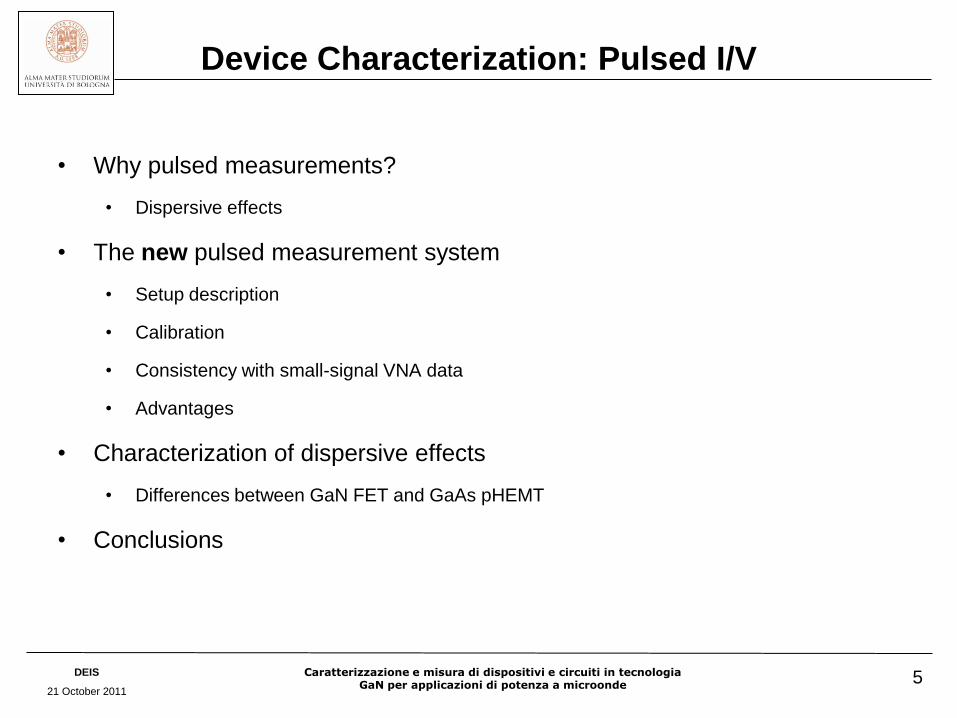
• Why pulsed measurements?
• Dispersive effects
• The new pulsed measurement system
• Setup description
• Calibration
• Consistency with small-signal VNA data
• Advantages
• Characterization of dispersive effects
• Differences between GaN FET and GaAs pHEMT
• Conclusions
5

DEIS
21 October 2011
Caratterizzazione e misura di dispositivi e circuiti in tecnologia GaN per applicazioni di potenza a microonde
Why pulsed I/V measurements?
• DC I/V characteristics affected by
dispersive phenomena
– Thermal self heating
– Charge trapping
6
Slow effects (long time constants)
• Extending SOA limits
DC vs Pulsed I/V
QUIESCENT
POINT strongly dependent on DC conditions

DEIS
21 October 2011
Caratterizzazione e misura di dispositivi e circuiti in tecnologia GaN per applicazioni di potenza a microonde
Why pulsed I/V measurements?
7
5 10 15 20 25 300 35
0.1
0.2
0.3
0.4
0.0
0.5
Vds [V]
Dra
in C
urr
en
t [A
]
Gv Dv
Di
Pulsed Output Characteristic
Gv
Dv* *,GS DSv vBIAS
*
DSv*
GSv
DEIS
21 October 2011
Caratterizzazione e misura di dispositivi e circuiti in tecnologia GaN per applicazioni di potenza a microonde
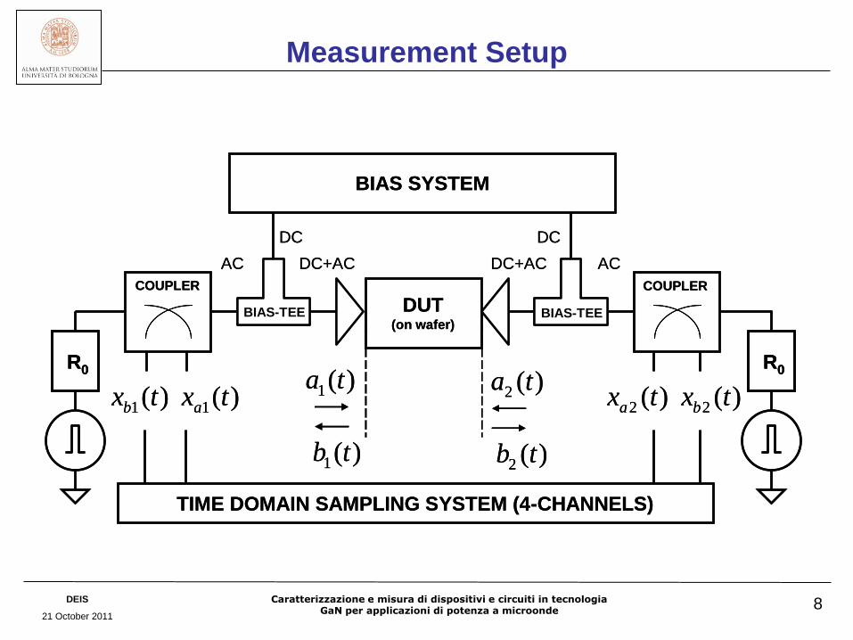
Measurement Setup
8
DUT(on wafer)
R0
1( )a t
1( )b t
1( )bx t 1( )ax t 2 ( )ax t 2 ( )bx t2 ( )a t
2 ( )b t
DC
AC DC+AC
BIAS SYSTEM
R0
DC+AC AC
DC
COUPLER COUPLER
BIAS-TEEBIAS-TEE
TIME DOMAIN SAMPLING SYSTEM (4-CHANNELS)
DUT(on wafer)
R0R0
1( )a t
1( )b t
1( )bx t 1( )ax t 2 ( )ax t 2 ( )bx t2 ( )a t
2 ( )b t
DC
AC DC+AC
BIAS SYSTEM
R0R0
DC+AC AC
DC
COUPLER COUPLER
BIAS-TEEBIAS-TEE
TIME DOMAIN SAMPLING SYSTEM (4-CHANNELS)

DEIS
21 October 2011
Caratterizzazione e misura di dispositivi e circuiti in tecnologia GaN per applicazioni di potenza a microonde
Measurement Setup
9
DUT(on wafer)
R0
1( )a t
1( )b t
1( )bx t 1( )ax t 2 ( )ax t 2 ( )bx t2 ( )a t
2 ( )b t
DC
AC DC+AC
BIAS SYSTEM
R0
DC+AC AC
DC
COUPLER COUPLER
BIAS-TEEBIAS-TEE
TIME DOMAIN SAMPLING SYSTEM (4-CHANNELS)
DUT(on wafer)
R0R0
1( )a t
1( )b t
1( )bx t 1( )ax t 2 ( )ax t 2 ( )bx t2 ( )a t
2 ( )b t
DC
AC DC+AC
BIAS SYSTEM
R0R0
DC+AC AC
DC
COUPLER COUPLER
BIAS-TEEBIAS-TEE
TIME DOMAIN SAMPLING SYSTEM (4-CHANNELS)

DEIS
21 October 2011
Caratterizzazione e misura di dispositivi e circuiti in tecnologia GaN per applicazioni di potenza a microonde
Measurement Setup
10
DUT(on wafer)
R0
1( )a t
1( )b t
1( )bx t 1( )ax t 2 ( )ax t 2 ( )bx t2 ( )a t
2 ( )b t
DC
AC DC+AC
BIAS SYSTEM
R0
DC+AC AC
DC
COUPLER COUPLER
BIAS-TEEBIAS-TEE
TIME DOMAIN SAMPLING SYSTEM (4-CHANNELS)
DUT(on wafer)
R0R0
1( )a t
1( )b t
1( )bx t 1( )ax t 2 ( )ax t 2 ( )bx t2 ( )a t
2 ( )b t
DC
AC DC+AC
BIAS SYSTEM
R0R0
DC+AC AC
DC
COUPLER COUPLER
BIAS-TEEBIAS-TEE
TIME DOMAIN SAMPLING SYSTEM (4-CHANNELS)

DEIS
21 October 2011
Caratterizzazione e misura di dispositivi e circuiti in tecnologia GaN per applicazioni di potenza a microonde
Measurement Setup
11
DUT(on wafer)
R0
1( )a t
1( )b t
1( )bx t 1( )ax t 2 ( )ax t 2 ( )bx t2 ( )a t
2 ( )b t
DC
AC DC+AC
BIAS SYSTEM
R0
DC+AC AC
DC
COUPLER COUPLER
BIAS-TEEBIAS-TEE
TIME DOMAIN SAMPLING SYSTEM (4-CHANNELS)
DUT(on wafer)
R0R0
1( )a t
1( )b t
1( )bx t 1( )ax t 2 ( )ax t 2 ( )bx t2 ( )a t
2 ( )b t
DC
AC DC+AC
BIAS SYSTEM
R0R0
DC+AC AC
DC
COUPLER COUPLER
BIAS-TEEBIAS-TEE
TIME DOMAIN SAMPLING SYSTEM (4-CHANNELS)
TRIG.

DEIS
21 October 2011
Caratterizzazione e misura di dispositivi e circuiti in tecnologia GaN per applicazioni di potenza a microonde
Measurement Setup
12
DUT(on wafer)
R0
1( )a t
1( )b t
1( )bx t 1( )ax t 2 ( )ax t 2 ( )bx t2 ( )a t
2 ( )b t
DC
AC DC+AC
BIAS SYSTEM
R0
DC+AC AC
DC
COUPLER COUPLER
BIAS-TEEBIAS-TEE
TIME DOMAIN SAMPLING SYSTEM (4-CHANNELS)
DUT(on wafer)
R0R0
1( )a t
1( )b t
1( )bx t 1( )ax t 2 ( )ax t 2 ( )bx t2 ( )a t
2 ( )b t
DC
AC DC+AC
BIAS SYSTEM
R0R0
DC+AC AC
DC
COUPLER COUPLER
BIAS-TEEBIAS-TEE
TIME DOMAIN SAMPLING SYSTEM (4-CHANNELS)
PA
TRIG.

DEIS
21 October 2011
Caratterizzazione e misura di dispositivi e circuiti in tecnologia GaN per applicazioni di potenza a microonde
Measurement Setup
13
DUT(on wafer)
R0
1( )a t
1( )b t
1( )bx t 1( )ax t 2 ( )ax t 2 ( )bx t2 ( )a t
2 ( )b t
DC
AC DC+AC
BIAS SYSTEM
R0
DC+AC AC
DC
COUPLER COUPLER
BIAS-TEEBIAS-TEE
TIME DOMAIN SAMPLING SYSTEM (4-CHANNELS)
DUT(on wafer)
R0R0
1( )a t
1( )b t
1( )bx t 1( )ax t 2 ( )ax t 2 ( )bx t2 ( )a t
2 ( )b t
DC
AC DC+AC
BIAS SYSTEM
R0R0
DC+AC AC
DC
COUPLER COUPLER
BIAS-TEEBIAS-TEE
TIME DOMAIN SAMPLING SYSTEM (4-CHANNELS)
THERMAL
CHUCK
Fully automated
through a
remote controlling
software
TRIG.
DEIS
21 October 2011
Caratterizzazione e misura di dispositivi e circuiti in tecnologia GaN per applicazioni di potenza a microonde
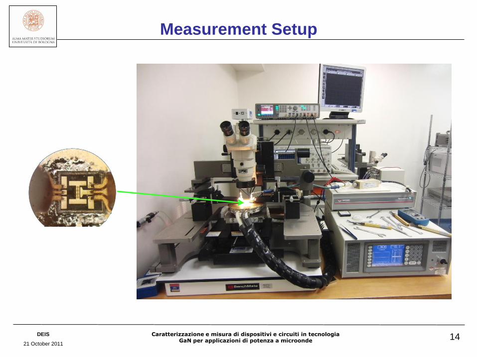
Measurement Setup
14
DEIS
21 October 2011
Caratterizzazione e misura di dispositivi e circuiti in tecnologia GaN per applicazioni di potenza a microonde
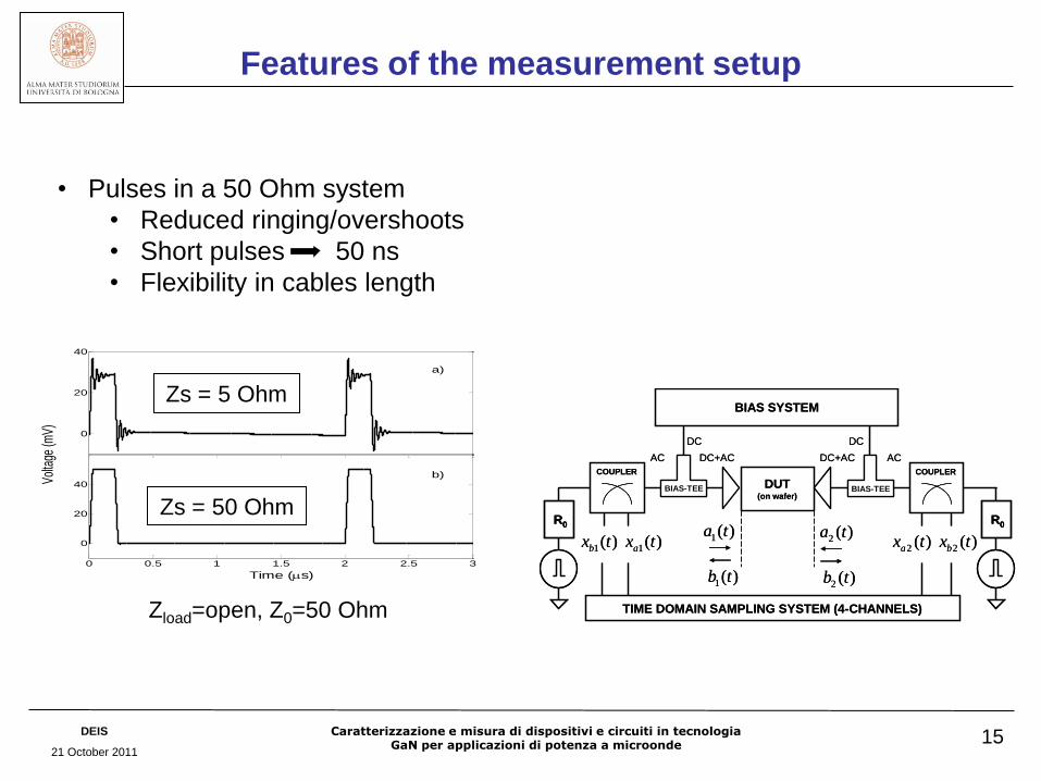
Features of the measurement setup
15
DUT(on wafer)
R0
1( )a t
1( )b t
1( )bx t 1( )ax t 2 ( )ax t 2 ( )bx t2 ( )a t
2 ( )b t
DC
AC DC+AC
BIAS SYSTEM
R0
DC+AC AC
DC
COUPLER COUPLER
BIAS-TEEBIAS-TEE
TIME DOMAIN SAMPLING SYSTEM (4-CHANNELS)
DUT(on wafer)
R0R0
1( )a t
1( )b t
1( )bx t 1( )ax t 2 ( )ax t 2 ( )bx t2 ( )a t
2 ( )b t
DC
AC DC+AC
BIAS SYSTEM
R0R0
DC+AC AC
DC
COUPLER COUPLER
BIAS-TEEBIAS-TEE
TIME DOMAIN SAMPLING SYSTEM (4-CHANNELS)
0
20
40
0 0.5 1 1.5 2 2.5 3
0
20
40
Time (s)
Volta
ge (m
V)
a)
b)
0
20
40
0 0.5 1 1.5 2 2.5 3
0
20
40
Time (s)
Volta
ge (m
V)
a)
b)
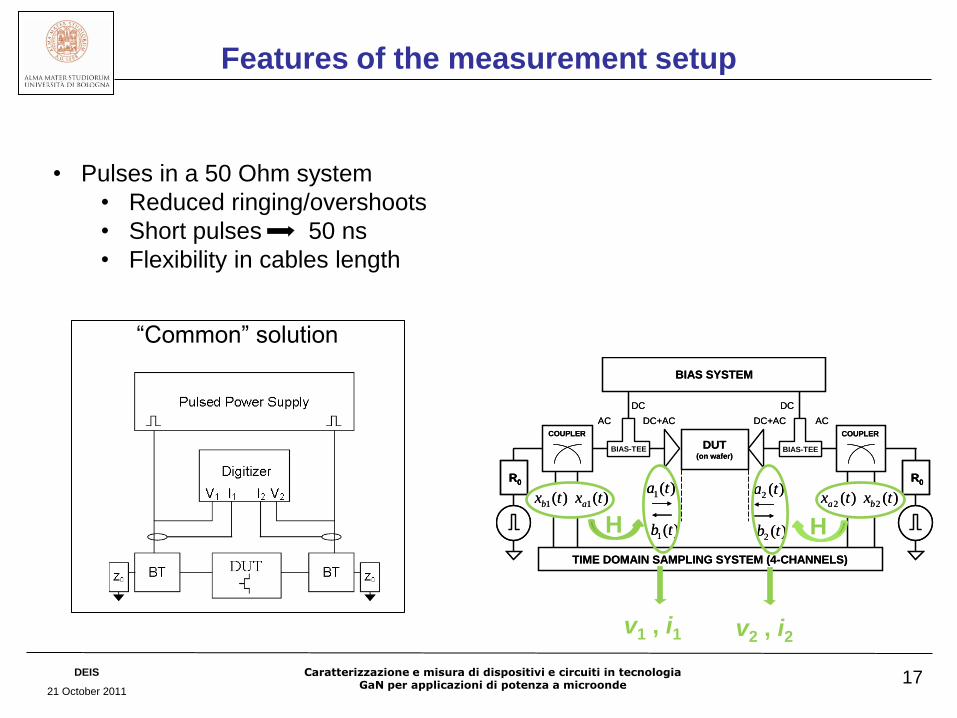
• Pulses in a 50 Ohm system
• Reduced ringing/overshoots
• Short pulses 50 ns
• Flexibility in cables length
Zs = 5 Ohm
Zs = 50 Ohm
Zload=open, Z0=50 Ohm

DEIS
21 October 2011
Caratterizzazione e misura di dispositivi e circuiti in tecnologia GaN per applicazioni di potenza a microonde
Features of the measurement setup
16
DUT(on wafer)
R0
1( )a t
1( )b t
1( )bx t 1( )ax t 2 ( )ax t 2 ( )bx t2 ( )a t
2 ( )b t
DC
AC DC+AC
BIAS SYSTEM
R0
DC+AC AC
DC
COUPLER COUPLER
BIAS-TEEBIAS-TEE
TIME DOMAIN SAMPLING SYSTEM (4-CHANNELS)
DUT(on wafer)
R0R0
1( )a t
1( )b t
1( )bx t 1( )ax t 2 ( )ax t 2 ( )bx t2 ( )a t
2 ( )b t
DC
AC DC+AC
BIAS SYSTEM
R0R0
DC+AC AC
DC
COUPLER COUPLER
BIAS-TEEBIAS-TEE
TIME DOMAIN SAMPLING SYSTEM (4-CHANNELS)
• Pulses in a 50 Ohm system
• Reduced ringing/overshoots
• Short pulses 50 ns
• Flexibility in cables length
“Common” solution
DEIS
21 October 2011
Caratterizzazione e misura di dispositivi e circuiti in tecnologia GaN per applicazioni di potenza a microonde
Features of the measurement setup
17
DUT(on wafer)
R0
1( )a t
1( )b t
1( )bx t 1( )ax t 2 ( )ax t 2 ( )bx t2 ( )a t
2 ( )b t
DC
AC DC+AC
BIAS SYSTEM
R0
DC+AC AC
DC
COUPLER COUPLER
BIAS-TEEBIAS-TEE
TIME DOMAIN SAMPLING SYSTEM (4-CHANNELS)
DUT(on wafer)
R0R0
1( )a t
1( )b t
1( )bx t 1( )ax t 2 ( )ax t 2 ( )bx t2 ( )a t
2 ( )b t
DC
AC DC+AC
BIAS SYSTEM
R0R0
DC+AC AC
DC
COUPLER COUPLER
BIAS-TEEBIAS-TEE
TIME DOMAIN SAMPLING SYSTEM (4-CHANNELS)
“Common” solution
H H
v1 , i1 v2 , i2
• Pulses in a 50 Ohm system
• Reduced ringing/overshoots
• Short pulses 50 ns
• Flexibility in cables length

DEIS
21 October 2011
Caratterizzazione e misura di dispositivi e circuiti in tecnologia GaN per applicazioni di potenza a microonde
Features of the measurement setup
18
• Ability of monitoring the average
drain current during the pulsed
characterization
Useful for understanding of
dispersion mechanisms in GaN
…as we will see..
• Pulses in a 50 Ohm system
• Reduced ringing/overshoots
• Short pulses 50 ns
• Flexibility in cables length
DUT(on wafer)
R0
1( )a t
1( )b t
1( )bx t 1( )ax t 2 ( )ax t 2 ( )bx t2 ( )a t
2 ( )b t
DC
AC DC+AC
BIAS SYSTEM
R0
DC+AC AC
DC
COUPLER COUPLER
BIAS-TEEBIAS-TEE
TIME DOMAIN SAMPLING SYSTEM (4-CHANNELS)
DUT(on wafer)
R0R0
1( )a t
1( )b t
1( )bx t 1( )ax t 2 ( )ax t 2 ( )bx t2 ( )a t
2 ( )b t
DC
AC DC+AC
BIAS SYSTEM
R0R0
DC+AC AC
DC
COUPLER COUPLER
BIAS-TEEBIAS-TEE
TIME DOMAIN SAMPLING SYSTEM (4-CHANNELS)
H H
IG0 ID0
v1 , i1 v2 , i2
DEIS
21 October 2011
Caratterizzazione e misura di dispositivi e circuiti in tecnologia GaN per applicazioni di potenza a microonde
DUT(on wafer)
R0
1( )a t
1( )b t
1( )bx t 1( )ax t 2 ( )ax t 2 ( )bx t2 ( )a t
2 ( )b t
DC
AC DC+AC
BIAS SYSTEM
R0
DC+AC AC
DC
COUPLER COUPLER
BIAS-TEEBIAS-TEE
TIME DOMAIN SAMPLING SYSTEM (4-CHANNELS)
DUT(on wafer)
R0R0
1( )a t
1( )b t
1( )bx t 1( )ax t 2 ( )ax t 2 ( )bx t2 ( )a t
2 ( )b t
DC
AC DC+AC
BIAS SYSTEM
R0R0
DC+AC AC
DC
COUPLER COUPLER
BIAS-TEEBIAS-TEE
TIME DOMAIN SAMPLING SYSTEM (4-CHANNELS)
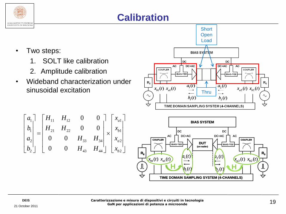
Calibration
• Two steps:
1. SOLT like calibration
2. Amplitude calibration
• Wideband characterization under
sinusoidal excitation
19
Short
Open
Load
Thru
11 12 11
21 22 11
33 34 22
43 44 22
0 0
0 0
0 0
0 0
a
b
a
b
H H xa
H H xb
H H xa
H H xb
H H

DEIS
21 October 2011
Caratterizzazione e misura di dispositivi e circuiti in tecnologia GaN per applicazioni di potenza a microonde
Consistency with small-signal VNA data
• If above cut-off conditions are met, the slopes of pulsed curves in the bias
point must coincide with differential parameters at the same bias point
20
• S-Parameters (@250 MHz) Y-Parameters
Output conductance:
Pulsed drain, fixed gate
0 2 4 6 8 100
10
20
30
40
50
60
Drain Voltage (V)
Dra
in C
urr
ent (m
A)
0 2 4 6 8 100
10
20
30
40
50
60
Drain Voltage (V)
Dra
in C
urr
ent (m
A)
GaAs PHEMT
(L=0.25 µm, W=300 µm)
Static (red)
Pulsed (blue)
from VG0=-0.5 V, VD0= 5 V
and VG0=-0.4 V, VD0= 5
Drain pulses only
gd ≈ ∆Id / ∆Vd
= 200 ns
δ = 10%
22
21
0 22
( )
1
d
m
g Y
Yg
R Y

DEIS
21 October 2011
Caratterizzazione e misura di dispositivi e circuiti in tecnologia GaN per applicazioni di potenza a microonde
Consistency with small-signal VNA data
Output conductance results:
21
Bias Output
Conductance from
Spar
at 250 MHz
(mS)
Output
Conductance from
pulsed I/V
(mS)
Relative
Difference
(%) VGS
(V)
VDS
(V)
-0.4 1.5 6,56 6,51 -0,76
-0.4 5 3,40 3,11 -8,5
-0.5 1.5 6,35 6,74 6,14
-0.5 5 3,34 3,21 3,89
-0.6 5 3.22 3,18 -1,2

DEIS
21 October 2011
Caratterizzazione e misura di dispositivi e circuiti in tecnologia GaN per applicazioni di potenza a microonde
GaAs Pulsed characteristic
22
1 2 3 4 5 6 7 8 90 10
20
40
60
80
100
120
0
140
Drain Voltage (V)P
uls
ed
Dra
in C
urr
en
t (m
A)
1 2 3 4 5 6 7 8 90 10
20
40
60
80
100
120
0
140
Drain Voltage (V)P
uls
ed
Dra
in C
urr
en
t (m
A)
-1.0 -0.8 -0.6 -0.4 -0.2-1.2 0.0
20
40
60
80
100
120
0
140
Gate Voltage (V)
Pu
lse
d D
rain
Cu
rre
nt
(mA
)
-1.0 -0.8 -0.6 -0.4 -0.2-1.2 0.0
20
40
60
80
100
120
0
140
Gate Voltage (V)
Pu
lse
d D
rain
Cu
rre
nt
(mA
)
GaAs PHEMT
(L=0.25 µm, W=300 µm)
DEIS
21 October 2011
Caratterizzazione e misura di dispositivi e circuiti in tecnologia GaN per applicazioni di potenza a microonde
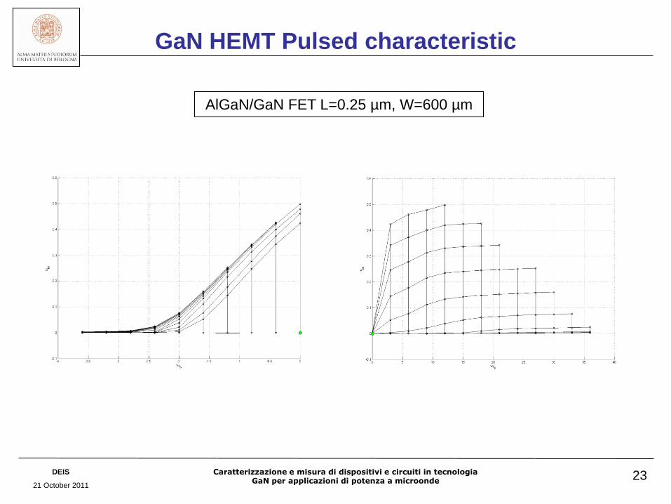
GaN HEMT Pulsed characteristic
23
AlGaN/GaN FET L=0.25 µm, W=600 µm

DEIS
21 October 2011
Caratterizzazione e misura di dispositivi e circuiti in tecnologia GaN per applicazioni di potenza a microonde
GaN Characterization of dispersive effects
Preliminary results and experiment:
• Pulsed drain-only excitation, gate kept constant at bias voltage.
• Pulsed measurements from 6 bias conditions:
– three gate voltages: VG0=-1.95V, VG0=-1.5V and VG0=-0.5V
– two drain voltages: VD0=15V and VD0=25V
• Pulse width: = 200 ns, duty: δ = 10%
• Constant baseplate temperature: Tb=36°C
24
AlGaN/GaN FET on SiC (L=0.25 µm, W=600 µm, IDSS ≅ 450 mA) on wafer

DEIS
21 October 2011
Caratterizzazione e misura di dispositivi e circuiti in tecnologia GaN per applicazioni di potenza a microonde
GaN Characterization of dispersive effects
25
AlGaN/GaN FET L=0.25 µm, W=600 µm
Total Drain
Current during
pulses
Average Drain
Current during
pulses
DEIS
21 October 2011
Caratterizzazione e misura di dispositivi e circuiti in tecnologia GaN per applicazioni di potenza a microonde
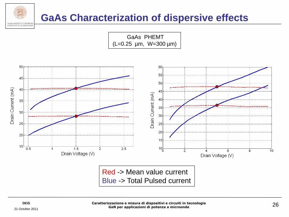
GaAs Characterization of dispersive effects
26
GaAs PHEMT
(L=0.25 µm, W=300 µm)
Red -> Mean value current
Blue -> Total Pulsed current

DEIS
21 October 2011
Caratterizzazione e misura di dispositivi e circuiti in tecnologia GaN per applicazioni di potenza a microonde
Overview: Bottom - Up
Pulsed I/V characterization
27
Device
Characterization
Device Modelling
Circuit Design
Circuit
Realization
Circuit
Measurement
S-parameters, static/pulsed IV, load pull, …
Device Model
layout
MMIC PA
Pout, PAE, …
Modeling of dispersive effects
in GaN devices
Design methodologies for GaN
Power Amplifiers
Measurement of GaN
Power Amplifiers
DEIS
21 October 2011
Caratterizzazione e misura di dispositivi e circuiti in tecnologia GaN per applicazioni di potenza a microonde
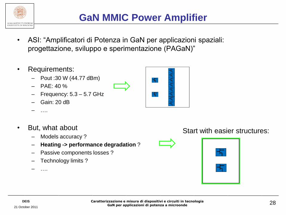
GaN MMIC Power Amplifier
• ASI: “Amplificatori di Potenza in GaN per applicazioni spaziali:
progettazione, sviluppo e sperimentazione (PAGaN)”
• Requirements: – Pout :30 W (44.77 dBm)
– PAE: 40 %
– Frequency: 5.3 – 5.7 GHz
– Gain: 20 dB
– ….
• But, what about – Models accuracy ?
– Heating -> performance degradation ?
– Passive components losses ?
– Technology limits ?
– ….
28
Start with easier structures:

DEIS
21 October 2011
Caratterizzazione e misura di dispositivi e circuiti in tecnologia GaN per applicazioni di potenza a microonde
GaN MMIC Power Amplifier
29
• Critical aspects
• passive components
• junction temperature
• current limits
• …

DEIS
21 October 2011
Caratterizzazione e misura di dispositivi e circuiti in tecnologia GaN per applicazioni di potenza a microonde
Measurement Setup
30

DEIS
21 October 2011
Caratterizzazione e misura di dispositivi e circuiti in tecnologia GaN per applicazioni di potenza a microonde
Measurement Setup
31

DEIS
21 October 2011
Caratterizzazione e misura di dispositivi e circuiti in tecnologia GaN per applicazioni di potenza a microonde
Measurement Setup
32

DEIS
21 October 2011
Caratterizzazione e misura di dispositivi e circuiti in tecnologia GaN per applicazioni di potenza a microonde
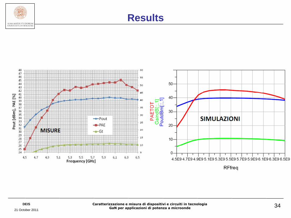
Results
33
SIM. MIS.
DEIS
21 October 2011
Caratterizzazione e misura di dispositivi e circuiti in tecnologia GaN per applicazioni di potenza a microonde
Results
34

DEIS
21 October 2011
Caratterizzazione e misura di dispositivi e circuiti in tecnologia GaN per applicazioni di potenza a microonde
GaN VS GaAs ( )
35
Costrini, et. al, "A Compact 8W S/C-Band MMIC Power Amplifier Designed for CW Telemetry
Applications," European Microwave Integrated Circuits Conference, 2006.
2 mm
2 mm
3.2 mm
4.2 mm
•Freq: 5.2 – 6.5 GHz
•Pout: 10 W
•PAE: 50 %
•Gain: 10 dB
•Area: 4 mm2
•Freq: 3.5 – 4.3 GHz
•Pout: 8 W
•PAE: 35 %
•Gain: 16 dB
•Area: 13.4 mm2

DEIS
21 October 2011
Caratterizzazione e misura di dispositivi e circuiti in tecnologia GaN per applicazioni di potenza a microonde
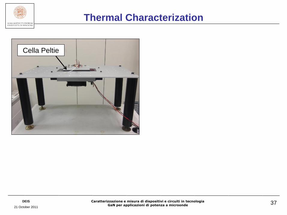
Thermal Characterization
36
Performance VS Tb
DEIS
21 October 2011
Caratterizzazione e misura di dispositivi e circuiti in tecnologia GaN per applicazioni di potenza a microonde
Thermal Characterization
37
Cella Peltie

DEIS
21 October 2011
Caratterizzazione e misura di dispositivi e circuiti in tecnologia GaN per applicazioni di potenza a microonde
Thermal Characterization
38
Cella Peltie

DEIS
21 October 2011
Caratterizzazione e misura di dispositivi e circuiti in tecnologia GaN per applicazioni di potenza a microonde
Thermal Characterization
39
Cella Peltie

DEIS
21 October 2011
Caratterizzazione e misura di dispositivi e circuiti in tecnologia GaN per applicazioni di potenza a microonde
Thermal Characterization
40
Cella Peltie

DEIS
21 October 2011
Caratterizzazione e misura di dispositivi e circuiti in tecnologia GaN per applicazioni di potenza a microonde
Conclusions
Current and Future works:
• Further investigation on charge trapping phenomena in GaN transistors
used as power amplifiers
• Non linear modeling of GaN transistor using pulsed I/V characteristics
• Thermal impedance extraction
41
• Demonstrated a new pulsed measurement system
• Features/advantages
• Calibration
• Pulsed measurements on GaN and GaAs devices
• A new way to watch at traps dispersive effects on GaN
• Design of a MMIC HPA in GaN
• Technology limitations
• Models validation
• Measurement setup -> performance degradation due to temperature variations

DEIS
21 October 2011
Caratterizzazione e misura di dispositivi e circuiti in tecnologia GaN per applicazioni di potenza a microonde
• A. Santarelli, R. Cignani, V. Di Giacomo, S. D’Angelo, D. Niessen, F. Filicori, “Large-signal characterization of GaN-based transistors for accurate nonlinear modelling of dispersive effects”, Proc. of 2010 Workshop on Integrated Nonlinear Microwave and Millimetre-wave Circuits (INMMiC 2010), Göteborg (Sweden), pp. 115-118, Apr 2010..
• A. Santarelli, V. Di Giacomo, R. Cignani, S. D’Angelo, D. Niessen, F. Filicori, “Nonlinear Thermal Resistance Characterization for Compact Electrothermal GaN HEMT Modelling”, Proc. of the 5th European Microwave Integrated Circuits conference (EuMIC 2010), pp. 82-85, 26 Sep-1 Oct 2010. EuMIC 2010 - Best Paper Award.
• A. Santarelli, R. Cignani, D. Niessen, S. D’Angelo, F. Filicori, “Electro-Thermal Characterization And Compact Modelling of GaN HEMTs for Microwave Applications”, Atti della 43a Riunione Annuale del Gruppo Elettronica (GE2011), pp. 93-94
• A. Santarelli, R. Cignani, D. Niessen, S. D’Angelo, P. A. Traverso, F. Filicori, “Characterization of GaN and GaAs FETs Through a New Pulsed Measurement System”, Proc. of the 6th European Microwave Integrated Circuits conference (EuMIC 2011), Oct 2011.
Pubblicazioni