TITOLO DELLA TESI: OFF-STATE RELIABILITY OF pGaN POWER …
75
Alma Mater Studiorum - Universit` a di Bologna campus di cesena DIPARTIMENTO DI INGEGNERIA DELL’ENERGIA ELETTRICA E DELL’INFORMAZIONE “GUGLIELMO MARCONI” CORSO DI LAUREA MAGISTRALE IN INGEGNERIA ELETTRONICA E TELECOMUNICAZIONI PER L’ENERGIA TITOLO DELLA TESI: OFF-STATE RELIABILITY OF pGaN POWER HEMTs Tesi di Laurea Magistrale in TECNOLOGIE ELETTRONICHE PER L’INFORMAZIONE E L’ENERGIA LM Relatore: Dr. ANDREA N. TALLARICO Correlatore: Dr. Ir. NIELS POSTHUMA Presentata da: MAURIZIO MILLESIMO III Sessione - II Appello Anno Accademico 2018/2019
Transcript of TITOLO DELLA TESI: OFF-STATE RELIABILITY OF pGaN POWER …

Alma Mater Studiorum - Universita di Bolognacampus di cesena
DIPARTIMENTO DI INGEGNERIA DELL’ENERGIA ELETTRICA E DELL’INFORMAZIONE“GUGLIELMO MARCONI”
CORSO DI LAUREA MAGISTRALE IN
INGEGNERIA ELETTRONICA E TELECOMUNICAZIONI PER L’ENERGIA
TITOLO DELLA TESI:
OFF-STATE RELIABILITY OF pGaN
POWER HEMTs
Tesi di Laurea Magistrale inTECNOLOGIE ELETTRONICHE PER L’INFORMAZIONE E
L’ENERGIA LM
Relatore:Dr. ANDREA N. TALLARICO
Correlatore:Dr. Ir. NIELS POSTHUMA
Presentata da:MAURIZIO MILLESIMO
III Sessione - II AppelloAnno Accademico 2018/2019


Acknowledgements
First of all, I would like to express my gratitude to my supervisor, Dr. A.N.Tallarico. I appreciate his guidance in the GaN devices world and, in partic-ular, in the reliability field. I would like to thank him especially to gave methe opportunity to do an internship at imec (Leuven, Belgium).
Special thanks to my daily supervisor at imec, Dr. Niels Posthuma for theinterest in my work and for the support given during my stay at imec.
Il piu grande ringraziamento va ai miei genitori. Grazie per aver credutosempre in me e per aver appoggiato ogni mia scelta.
Thank you all,Maurizio
i
Abstract
The concern for climate changes and the increase in the electricity demandturned the attention towards the production, sorting and use of electric en-ergy through zero emission (CO2) and highly efficient solutions (e.g. forelectric vehicle), respectively. In such a scenario, power converters and/orinverters play a fundamental role, since they represent the main core of powerapplications. As a consequence, the need for high performance, reliable andlow cost power transistors is increasing as well. The most used semiconductormaterials for power transistors are three: silicon (Si), silicon carbide (SiC)and gallium nitride (GaN). Among all of them, gallium nitride, seems to bethe most promising candidate for the next generation of devices for powerelectronics, thanks to its excellent properties and comparable cost with re-spect to Si counterpart. The main and most adopted GaN-based device isthe high electron mobility transistor (HEMT). In particular, in the case ofswitching power applications, HEMTs are repeatedly switched between highcurrent on-state and high voltage off-state operation. For both operatingmodes a good reliability must be guaranteed.This thesis is focused on the reliability issues related to the off-state oper-ation. The results have been obtained during a six months research periodat imec (Leuven, BE) on 200V p-GaN gate AlGaN/GaN HEMTS. Differ-ent devices have been investigated, differing for gate-to-drain distance, fieldplates lengths, AlGaN and GaN layers properties. Time-dependent dielectricbreakdown and hard breakdown tests have been performed in combinationwith TCAD simulations. It has been demonstrated that the gate-to-draindistance (L
GD) impacts the breakdown voltage and the kind of failure mech-
anism. If LGD ≤ 3µm the breakdown occurs through the GaN channel layerdue to short channel effects. In this case, by reducing the thickness of theGaN channel layer such behaviour can be attenuated, eventually leading tolonger time-to-failure. If LGD ≥ 4µm the breakdown occurs between the2DEG and the source field plates, where the properties of the AlGaN barrierlayer (i.e. thickness and Al concentration) and the field plates configurationplay the main role on the time-to-failure.
ii

Contents
Acknowledgements i
Abstract ii
1 Introduction 11.1 Semiconductor Power Devices Technologies . . . . . . . . . . . 2
1.1.1 Material Properties . . . . . . . . . . . . . . . . . . . . 31.1.2 Figure Of Merit (FOM) . . . . . . . . . . . . . . . . . 41.1.3 Breakdown Voltage and On Resistance . . . . . . . . . 5
2 III-N materials and devices 82.1 Substrates for III-N Epitaxy . . . . . . . . . . . . . . . . . . . 92.2 III-N Crystal Structures and Polarization Effects . . . . . . . . 102.3 Metal-Organic Vapor Phase Deposition for III-Nitride Epi-
layer Deposition on Si . . . . . . . . . . . . . . . . . . . . . . 132.3.1 The Nucleation Layer . . . . . . . . . . . . . . . . . . . 152.3.2 The Buffer Layer for Mechanical Stress Management . 152.3.3 AlGaN/GaN Heterostructure and 2DEG Formation . . 162.3.4 Top Part of HEMT: from Capping to Surface Passiva-
tion Layers . . . . . . . . . . . . . . . . . . . . . . . . 182.4 Lateral GaN Devices for Power Application . . . . . . . . . . 20
2.4.1 Cascode Configuration: GaN + Si . . . . . . . . . . . 202.4.2 E-mode GaN-based Transistor . . . . . . . . . . . . . . 21
Summary . . . . . . . . . . . . . . . . . . . . . . . . . . . . . . . . 24
3 GaN Reliability Issues 263.1 Trapping effects . . . . . . . . . . . . . . . . . . . . . . . . . . 273.2 On-State Degradation Mechanisms . . . . . . . . . . . . . . . 283.3 Semi-On-State Degradation Mechanisms . . . . . . . . . . . . 303.4 Off-State Degradation Mechanisms . . . . . . . . . . . . . . . 31
3.4.1 Vertical Leakage/Breakdown . . . . . . . . . . . . . . . 32
iii

3.4.2 Lateral Breakdown in the Gate-Drain Region . . . . . 333.4.3 Lateral Breakdown between Source and Drain . . . . . 35
Summary . . . . . . . . . . . . . . . . . . . . . . . . . . . . . . . . 36
4 Investigation of the Off-State Reliability on 200V pGaN HEMTs 384.1 Experimental Details . . . . . . . . . . . . . . . . . . . . . . . 38
4.1.1 Device Under Test . . . . . . . . . . . . . . . . . . . . 394.1.2 Hard Breakdown . . . . . . . . . . . . . . . . . . . . . 404.1.3 Time-Dependent Dielectric Breakdown (TDDB) . . . . 41
4.2 Results and Discussion . . . . . . . . . . . . . . . . . . . . . . 454.2.1 Role of the AlGaN on off-state reliability. . . . . . . . . 494.2.2 From surface to bulk failure . . . . . . . . . . . . . . . 52
Conclusion . . . . . . . . . . . . . . . . . . . . . . . . . . . . . . . . 56
Bibliography 58
iv


Chapter 1
Introduction
With increasing world population and the request for higher living standard,the demand for electricity is increasing as well. The worldwide electricitycan be produced by the adoption of different sources as shown in figure 1.1,with fossil fuels representing the most adopted ones.
Figure 1.1: Worldwide electricity production by various sources [1].
The earth has large reserves of fossil fuels, however, their adoption re-sults in waste products, which added to those produced for transport, do-mestic heating, etc. represent the main source of pollution that contribute
1

to climate change problem. To this purpose zero-emission solutions are be-ing implemented to protect the environment (e.g. electricity production bymeans of renewable sources and replacement of powered fuels vehicles withelectric/hybrid engines).In this scenario, power electronics plays an important role since most of theelectricity is controlled by semiconductor power devices. Today, with theadvancement of technology, the size and the price of semiconductor powerdevices are decreasing, leading power electronics to cover a wide range ofapplication fields such as aerospace, automotive, energy saving, industrial,commercial, smart houses, etc..
1.1 Semiconductor Power Devices Technolo-
gies
Until a few years ago, the semiconductor power devices market was com-pletely dominated by the mature silicon (Si) technology because of the lowcost and good reliability.However, with the increasing demand for lightweight,compact and evermore efficient power applications, the intrinsic limits of Si(i.e. limited switching frequency, blocking voltage and temperature capabil-ity [2]) arise the need to move towards wide bandgap semiconductors, likegallium nitride (GaN) and silicon carbide (SiC), that exhibit superior mate-rials properties compared to silicon counterpart.
Figure 1.2: Application fields of the different technologies (Si, SiC and GaN)as a function of operating frequency and power [3].
2

In figure 1.2 the application fields of Si, SiC and GaN power devices areshown as function of the operating power and switching frequency. In partic-ular,SiC and GaN are the best candidates for high voltage and high frequencyoperation, respectively, while silicon still preferred for low voltage and lowfrequency operation.The reason of this division will be further supported inthe section 1.1.1.
1.1.1 Material Properties
The application field of Si, SiC and GaN strongly depend on their intrinsicmaterial properties which are useful for switching power applications. Inparticular the most important characteristics are [4], [2]:
• bandgap: wider bandgap implies lower intrinsic carrier concentration(ni), which is strongly dependent on the temperature and correlated toleakage current [2]. As a consequence, wider bandgap allows devices tooperate at higher temperatures;
• critical electric field: higher critical field means that the impact ion-ization, hence the avalanche-induced breakdown, occurs at higher volt-ages;
• thermal conductivity: larger thermal conductivity implies that the de-vice can withstand a higher power density;
• carrier velocity saturation: higher carrier saturation velocity implies ahigher frequency of switching at higher voltages (Jhonson’s FOM [4]).
• electron mobility: higher electron mobility leads to lower resistivity andconduction losses;
Table 1.1 shows the various key material parameters for power electronics ofthe different materials for power electronics. GaN and SiC feature a bandgap∼3 times higher than Si which lead to have higher electric breakdown field(EC) and lower intrinsic carrier concentration useful to have negligible leakagecurrents at high operation temperature. Among all the materials, SiC hasthe highest thermal conductivity making it the best choice for high voltageand power operation, while, GaN is the best candidate for high frequencyand high current operations since it has the highest electron mobility (µ) andvelocity saturation (vsat). Finally, for low voltage and frequency applicationssilicon is the best choice thanks to its low cost and reliability, even though ithas less attractive features for power electronics compared to GaN and SiC.
3

Parameter Units Si GaAs 4H-SiC GaNBandgap (EG) eV 1.12 1.42 3.26 3.49Intrinsic carrierconcentration(ni)
/cm3 1.4x10¹⁰ 2.1x10⁻⁶ 8.2x10⁻⁹ 1.9x10⁻¹⁰
Electric break-down field (EC)
MV/cm 0.23 0.4 2.2 3.3
Saturated elec-tron velocity(vsat)
cm/s 1x10⁷ 1x10⁷ 2x10⁷ 2.5x10⁷
Thermal con-ductivity (k)
W/cm-k 1.5 0.5 3.8 1.53
Electron mobil-ity (µ)
cm2/V-sec 1400 8500 950 1800
Relative dielec-tric constant(εr)
- 11.8 12.8 9.7 9
Table 1.1: Comparison of material properties among different semiconductors[4].
1.1.2 Figure Of Merit (FOM)
The choice of a semiconductor for the realization of a power device is madeconsidering several figures of merit [5], which are related to the material prop-erties discussed in the section 1.1.1. The Johnson’s figure of merit (JFOM) [6]defines a value for the high frequency handling capability of a semiconductorbeing proportional to the saturation velocity and critical electric field:
JFOM =EC · vsat
2π(1.1)
The high power handling capability is described by Baliga’s figure of merit(BFOM) [7] that quantifies the conduction losses in DC operation, which iscalculated based on the relative electric permittivity (εr), electron mobility(µ) and bandgap (EG):
BFOM = εr · µ · E3G (1.2)
Instead, to quantify the conduction losses in high frequency operation, andtherefore, to evaluate the high power and frequency performance the Baliga’sHigh Frequency FOM (BHFFOM) is used [5]:
BHFFOM = µ · E2C (1.3)
4
Considering these three FOMs, among the semiconductors taken into con-sideration, gallium nitride has the best performance although silicon carbidefeatures similar FOMs, while, silicon and gallium arsenide have too low FOMfor power applications.SiC is the semiconductor that has the best Keyes FOM (KFOM) [5] becausetakes into account the thermal conductivity (k) and it describes the thermalperformance of the devices during switching operation:
KFOM = k ·√c · vsat4πεr
(1.4)
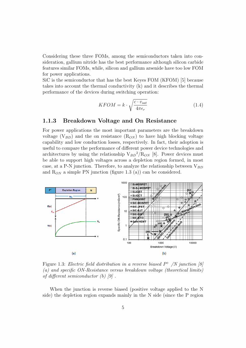
1.1.3 Breakdown Voltage and On Resistance
For power applications the most important parameters are the breakdownvoltage (VBD) and the on resistance (RON) to have high blocking voltagecapability and low conduction losses, respectively. In fact, their adoption isuseful to compare the performance of different power device technologies andarchitectures by using the relationship VBD
2/RON [8]. Power devices mustbe able to support high voltages across a depletion region formed, in mostcase, at a P-N junction. Therefore, to analyze the relationship between VBD
and RON a simple PN junction (figure 1.3 (a)) can be considered.
Figure 1.3: Electric field distribution in a reverse biased P+ /N junction [8](a) and specific ON-Resistance versus breakdown voltage (theoretical limits)of different semiconductor (b) [9] .
When the junction is reverse biased (positive voltage applied to the Nside) the depletion region expands mainly in the N side (since the P region
5
is strongly doped) with the consequently generation of a strong electric field.As shown in figure 1.3 (a) the peak of the electric field occurs in the proximityof the PN junction and, according to Poisson’s equation, it can be computedas follow [8]:
Emax =qNDWD
ε0εr(1.5)
where ND and WD are the doping concentration and the maximum extensionof the depletion region, while,ε0 andεr are the dielectric vacuum constant andthe dielectric constant relative to the material, respectively.Any electrons or holes that enter the depletion region are swept out by theelectric field and as the electric field increase the mobile carriers are pushedout with a higher velocity. If the electric fields is sufficiently high, electronsand holes acquire sufficient kinetic energy to create new electron-hole pairsdue to energy loss caused by interaction with the lattice. This phenomenon,namely, impact ionization is a multiplicative mechanism which produces anincreasing amount of mobile charges with a consequent increase in the currentthrough the depletion region. This latter leads to the avalanche breakdownthat strongly depends on the applied electric field and it occurs when theEmax approaches to the critical electric field (EC). The occurrence of thelatter condition defines the breakdown voltage, defined as:
VBD =1
2ECWD =
1
2
qNDW2D
ε0εr(1.6)
The specific ON resistance, which is mainly dominated by the resistive com-ponent of the N-drift region in ON-State operation is equal to:
RON,sp = ρWD =WD
qµnND
(1.7)
Replacing WD and ND from Eq. 1.5 and Eq. 1.6 into Eq. 1.7 it is pos-sible notice the mutual dependence between ON-resistance and breakdownvoltage::
RON,sp =4V 2
BD
ε0εrµnE3C
(1.8)
Being RON and VBD dependent from the intrinsic properties of the ma-terials, it is possible to analytically calculate the theoretical limits for eachsemiconductor-based technology, as shown in figure 1.3 (b). By observingFig. 1.3(b), it is worth noting that the theoretical limits are computed con-sidering only the ON resistance of the drift region, which dominant but notthe only one, devices are far away from their theoretical limits. Moreover, in
6
the case of GaN-devices this difference can be even larger since the break-down voltage during OFF-state operation can be caused by additional failuremechanisms (detailed in the next chapter), anticipating the breakdown in-duced by impact ionization.
7

Chapter 2
III-N materials and devices
Gallium nitride and its related alloys (e.g. AlxGa1−xN) are promising candi-dates for the next generation of high power and high frequency devices dueto their excellent material properties. As already mentioned, the wide bandgap of these materials leads to have a low intrinsic concentration and, conse-quently, a low leakage current that allows high temperature operation. An-other important feature of GaN is the high breakdown voltage which resultsin the possibility to fabricate smaller devices, hence characterized by lower onresistance and lower parasitics (mainly capacitances) which can be detrimen-tal for both static and dynamic operation operation mode. Compared to theirsilicon counterparts, GaN-based devices have a higher switching frequencydue to combined effect of higher carriers velocity saturation and smaller area,and a lower resistance due to the high mobility of the two dimension electrongas (2DEG) that appears in the AlGaN/GaN heterostructure [10],[11]. TheAlGaN/GaN heterostructure is the main core of the GaN transistors, namelyhigh electron mobility transistor (HEMT), where the electron current flowsthrough the 2DEG from source to drain contacts.Producing an emerging micro-scaled semiconductor device, the control andmastering of thin film techniques are essential. This includes metallization,dielectric layers, passivation layers or high quality crystalline functional lay-ers. The crystalline layers are deposited by epitaxy starting from the sub-strate. Usually, the substrate and the crystalline layer are made of differentmaterials characterized by different lattice constants and thermal expansioncoefficients. This situation is usually called heteroepitaxy that leads to con-sequences like the formation of threading dislocation, buildup of strain, andreliability issues. These physical consequences, that involve reliability prob-lems for the devices, could be reduced using homoepitaxy (epitaxy with samematerials) but, unfortunately, nature does not provide GaN bulk crystal.Although some GaN wafers grown with HVPE [12] showed extremely low
8

residual impurity concentration , the challenges of high cost and small waferdiameter remain open. Moreover, homoepitaxy has a lot of mismatch issuesdue to the different growth processes of the GaN layer. The only alternativeis to look for foreign materials for substrates that have lattice parameters andcrystal structures and orientation close to GaN material. Native substratesare mandatory only for some specific applications who claim high reliability(like in the case of blue and ultraviolet semiconductor lasers) since optimiz-ing the design of the devices it is possible to achieve a good reliability [13].Despite its incredible characteristics, gallium nitride has many issues as thepresence of nitrogen or the lack of a native substrate that will be discussedin along this chapter.
2.1 Substrates for III-N Epitaxy
The choice of substrate and material for GaN-based devices strongly dependson the field of application. Today, GaN wafers can be manufactured, but,have high costs and are only avaiable with limited wafer diameters, maximum2 inch. GaN is very difficult to growth as a single crystal since it is stronglycovalent bonded and contain nitrogen (N) that cannot be melted due to itshigh melting point above 2000◦C and high equilibrium pressure around 60kbar; moreover, the solubility of nitrogen in a pure gallium melt is very low[14]. This makes it impossible to grow a GaN crystal with classical melt-based methods like Czochralski pulling, vertical gradient freeze technique,etc. Today, the GaN wafers (expensive and size-limited) are manufacturedwith solution growth methods (addition of solvent to improve the solubility)and the GaN is crystalized from the vapor phase with two main methods:HVPE (hydride vapor phase epitaxy) and OVPE (oxide vapor phase epi-taxy).To overcome these limitations and to reduce the overall device costs, GaNdevices are currently and mainly grown on foreign substrates.For optoelectronics, sapphire is the best choice since it has a good matchto GaN in terms of lattice constants and thermal expansion coefficient. Fur-thermore, sapphire substrates are transparent, cheap and they have the samethreading dislocation densities as the Si and SiC substrates (2.1). As disad-vantages, sapphire has low thermal conductivity and insulating properties,making it less attractive for power electronic applications in order to preventoverheating and premature device failure [15]. Sapphire wafers exist in largediameters, but layers growth on large area is challenging due to the waferbowing and/or cracking after cooling because of tensile stress for betweenepitaxial layers.
9

Sapphire SiC Si GaNLattice mismatch (percent-age)
16 3.1 -17 0
Linear thermal expansioncoefficient (x10−6 K−1)
7.5 4.4 2.6 5.6
Thermal conductivity (Wcm−1 K−1 )
0.25 4.9 1.6 2.3
Cost Low High VeryLow
VeryHigh
Table 2.1: Properties for different substrates for GaN epitaxy [14], [16].
Among the three foreign substrates reported in table 2.1, SiC is the onewith the best matched mechanical properties with GaN. It is available bothas n-type and semi-insulating material and it has high thermal conductivitywhich makes it the best candidate for electronic applications with high powerdensities. As drawbacks, it has very high costs of fabrication and and thelargest available wafer diameters are 6 inch.For GaN heteroepitaxy, the most used material for the substrates is siliconbecause of its lowe cost and compatibility with CMOS technology. Epitax-ial growth of GaN directly on Si substrates is more challenging than het-eroepitaxy on sapphire or silicon carbide due to large lattice and thermalmismatches that results in large strain accumulation in the upper III-N epi-layers. This problem, if not properly monitored, leads to wafer deformation,cracking up to breakage, threading dislocations, etc. However, the advan-tages of a low substrate cost, large substrate diameter availability (up to12 inches), reasonable thermal conductivity and the possibilities of the co-integration with Si-CMOS electronics, make Si substrate the preferred choicefor a large set of power electronics (mostly medium range voltage) [17].
2.2 III-N Crystal Structures and Polarization
Effects
Group III nitrides compound (III-N) exist in different crystal forms likezincblende, rocksalt and wurtzite structures [11]. Among these forms thewurtzite crystal structure features the highest thermo-dynamical stability.Wurtzite-type GaN is composed of two hexagonal lattices of N and Ga asshown in figure 2.1, where c-axis is the most preferred growth direction. GaN
10

can be grown with two different polarities, i.e. Ga-face and N-face shown inFig. 2.1.
Figure 2.1: Crystal structure of wurtzite Ga-face and N-face GaN [11] .
In the case of Ga-face, the bonds along the [0001] direction are directedfrom Ga to N atoms, while, for N-face GaN the bonds along the [0001] direc-tion are from N to Ga atoms. The growth of Ga-face GaN is usually carriedout using Metal Organic Chemical Vapor Deposition, while N-face GaN canbe grown by Molecular Beam Epitaxy [13]. Both N-face GaN and Ga-faceGaN possess spontaneous polarization (PSP ) properties along c-axis due tocharge transfer between atoms with different electronegativity, as in the caseof Ga (lower) and N (higher) [10], [11].The III-nitride materials cover a very large range of bandgap energies, start-ing from infrared (InN with a bandgap of 0.7 eV) up to the extreme ultravi-olet (with AlN having a bandgap of 6.2 eV), as shown in figure 2.2. This ispossible by varying the concentrations of the group-III elements (Al, Ga, In)in the crystal alloy with a composition AlxInyGa1−x−yN with x,y and x+ybetween 0 and 1.
11

Figure 2.2: Bandgap versus lattice constant of III-N materials [18].
In GaN-based devices is common to find heterostructures with differentlattice constant, for instance AlGaN/GaN heterojunction in HEMTs. Whenthe AlGaN is grown on the GaN layer the different lattice constant leads toa mechanical stress causing a new type of polarization along c-axis, namelypiezoelectric polarization. The latter is due to the lattice constant adjustmentof the thinner material (AlGaN in this case). The amount of piezoelectricpolarization is given by [10], [11]:
PPE = 2a− a0a0
(e31 − e33C13
C33
) (2.1)
where e31 and e33 are piezoelectric constants, C13 and C33 are the elasticdeformation constants, a0 and a are the horizontal lattice constant before andafter the mechanical stress, respectively. The orientation of the spontaneouspolarization is defined positive from Ga (cation) to nearest nitrogen atom(anion) along the c-axis, whereas the piezoelectric polarization is assumednegative for tensile and positive for compressed strained AlGaN barriers.Therefore, both polarizations are parallel in the case of tensile strain, whileantiparallel in the case of compress strain of the AlGaN barrier. In the case ofthe AlGaN/GaN heterostructures, where the AlGaN barrier is grown on GaNlayer, both polarizations point in the same direction and the value of totalpolarization is the sum of the piezoelectric and spontaneous polarization.
12

The presence of these polarizations lead to creation of a channel of electronsat the AlGaN/GaN interface, namely two dimensional electron gas (2DEG),without the application of external biases. Further details on the 2DEGformation are reported in the subsection 2.3.3.
2.3 Metal-Organic Vapor Phase Deposition
for III-Nitride Epilayer Deposition on Si
The most suited technique for III-N epilayer deposition is the metal-organicchemical vapor deposition (MOCVD), also called metal-organic vapor phaseepitaxy (MOVPE). By using this technique, the elements of the growing ma-terial are introduced in a reactor chamber in gaseous form, transported by acarrier gas like nitrogen (N2) or hydrogen (H2) or a mixture of both. Indeed,the atoms of a given material are introduced in the chamber as precursor,that, for the III elements are a combination of the III group metals withorganic elements. The source compounds for gallium are typically trimethyl-gallium (CH3)3Ga and triethylgallium (C2H5)3Ga, while, the precursor fornitrogen is ammonia (NH3) where the nitrogen atom is directly bonded tohydrogen atoms. These molecules are first thermally decomposed and thenthey react, in the gas phase, on the substrate’s surface or on another III-Nsemiconductor layer. The epitaxial growth process is monitored thermody-namically, i.e., by setting temperature and pressure of both the substrate andambient for the gas in the reactor. The difference between the two energiescan provide etching of the below layer or growth of the semiconductor on thesurface. Usually, for GaN growth the temperature of the process is around1000oC and the reactor pressure between 10 mbar and 200 mbar. It is im-portant that there is always equilibrium between the gas phase compositionand the vapor pressure of the molecules of the solid phase to avoid contam-ination, since any contamination in the gas phase induces contamination ofthe solid semiconductor material. The contaminants atoms, such as carbonand hydrogen, could come from the metal-organic precursor themselves andit requires a good control of the vapor pressure to reduce inclusion of thisatoms in the solid phase. [19]The residual impurities, formed during the MOCVD processes, can play animportant role in the layer’s conductivity since they can have donor or accep-tor dopant behavior. Through MOCVD, a further intentional doping can beobtained by introducing other precursor in the initial gas mixture. The bestchoice for the p-type doping in GaN is the magnesium and, it is providedby the precursor biscyclopentadienyl magnesium (Cp2Mg) [20]. While, the
13

n-type doping is obtained by silicon via addition of silane (SiH4) or disilanein the chamber(Si2H6) [21]. In the GaN based HEMTs the active part ofthe devices don’t need any doping, but, doping can be used for increase theresistivity of a given layer (e.g. buffer), to decrease the gate ohmic contactresistance (n-type doping) or to compensate the intrinsic n-type behavior ofIII-nitrides (p-type doping).
Figure 2.3: General structure for an AlGaN/GaN HEMT device on Si.
In the following subsections will be described, layer-by-layer, the structureof the GaN based later HEMTs on Si substrate, as shown in figure 2.3. Themain parts are the following:
1. A nucleation layer to initiate the epitaxial growth on the foreign Sisubstrate.
2. A buffer stack to compensate mechanical differences between Si andGaN.
3. The AlGaN/GaN heterostructure with the final capping to protect thesurface, also called passivation layer.
14

2.3.1 The Nucleation Layer
As discussed in the previous sections, there are many issues related to grow-ing a high quality GaN crystal on Si substrate due to thermal and latticemismatch. Monocrystalline silicon and GaN have a cubic and hexagonal crys-tal structure, respectively. This difference may lead to a roughness GaN/Siinterface and consequent lower quality of the buffer microstructure [22]. Fur-thermore, at high temperature gallium easily diffuse into silicon substrateleading to gallium silicide formation. This phenomenon is called galliummelt-back etching and, to prevent it, the best solution is to deposit an AlNlayer on the substrate [19].The growth conditions and properties of the nucleation layer can influencethe final GaN film quality and the breakdown voltage in HEMTs. Manystudies reported that the electrical breakdown does not occur laterally butvertically [23]. This effect is attributed to vertical path for electron fromohmic drain contact to substrate due to multiple threading dislocations, alateral conduction along the AlN/Si interface followed by another verticalconduction between substrate and source trough dislocations/defects. AlNlayer thickness is the most important key parameter to improve the break-down voltage and the crack densities into the upper III-N layers [24].
2.3.2 The Buffer Layer for Mechanical Stress Manage-ment
The nucleation layer is not sufficient to prevent cracking in the GaN channellayer or wafer bow during cool down of the wafer and, for this reason, it isnecessary a buffer stack between AlN layer and the GaN channel for strainmanagement. The growth of GaN directly on AlN showed some circular de-fects, probably due to silicon outdiffusion from substrate, that could act asstress concentrators and initiate the cracking [22]. One of the first adoptedsolutions was based on the interposition of a single AlGaN layer with a grad-ual decrease of Al concentration from the top to the bottom, as shown infigure 2.4 (a). This latter shows some circular defects close to the edge ofthe wafer very similar to those seen growing GaN directly on relatively thickAlN layer.Another approach consists in the fabrication of a multiple layer buffer witha gradual relaxing of the strain due to the differences in lattice constants ofthe materials. One of the best method is called step-graded buffer [25] andconsist in growing AlGaN layers with different Al concentrations, graduallylower from AlN to GaN , shown in figure 2.4 (b). This procedure is repeatedfrom two to five times until finally a smooth and free-crack GaN layer can be
15

grown. This procedure leads to a gradually increase in the lattice constantand the quality of the final GaN layer improves by increasing the number ofthe AlGaN layers.
Figure 2.4: Structure of HEMTs with different buffer stack on Si sub-strate: (a) graded AlGaN layer, (b) multiple step-graded AlGaN layers wherex<y<z<k, (c) AlN/GaN superlattice buffer.
Besides the step-graded buffer, the most commonly used approach is thesuperlattice buffer, as shown in figure 2.4 (c). The superlattice stack is man-ufactured alternating dozens of relative thin GaN and AlN layers [26]. Alsoin this case, by increasing the number of interlayers the final GaN crystalquality increases as well, meaning that there is a higher probability that ver-tically propagating threading dislocation eventually annihilate at the surfacesbetween the multiple layers.Finally, after the buffer for strain management a final layer of carbon dopedGaN is added (not showed in figure 2.4). The latter serves to increase thevertical breakdown voltage, to suppress punch-through in the off-state op-eration and to improve the normally-off operation without changes in theON-resistance. More details can be found in [27] and [28].
2.3.3 AlGaN/GaN Heterostructure and 2DEG Forma-tion
GaN electronics are mostly based on the HEMT structure, with the activepart is composed by an AlGaN/GaN heterostructure. After nucleation layerand strain management buffer a GaN channel layer followed by a thinner
16
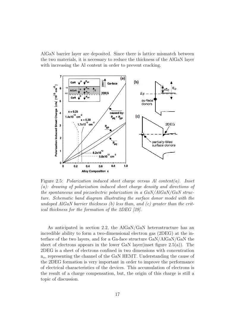
AlGaN barrier layer are deposited. Since there is lattice mismatch betweenthe two materials, it is necessary to reduce the thickness of the AlGaN layerwith increasing the Al content in order to prevent cracking.
Figure 2.5: Polarization induced sheet charge versus Al content(a). Inset(a): drawing of polarization induced sheet charge density and directions ofthe spontaneous and piezoelectric polarization in a GaN/AlGaN/GaN struc-ture. Schematic band diagram illustrating the surface donor model with theundoped AlGaN barrier thickness (b) less than, and (c) greater than the crit-ical thickness for the formation of the 2DEG [29].
As anticipated in section 2.2, the AlGaN/GaN heterostructure has anincredible ability to form a two-dimensional electron gas (2DEG) at the in-terface of the two layers, and for a Ga-face structure GaN/AlGaN/GaN thesheet of electrons appears in the lower GaN layer(inset figure 2.5(a)). The2DEG is a sheet of electrons confined in two dimensions with concentrationns, representing the channel of the GaN HEMT. Understanding the cause ofthe 2DEG formation is very important in order to improve the performanceof electrical characteristics of the devices. This accumulation of electrons isthe result of a charge compensation, but, the origin of this charge is still atopic of discussion.
17
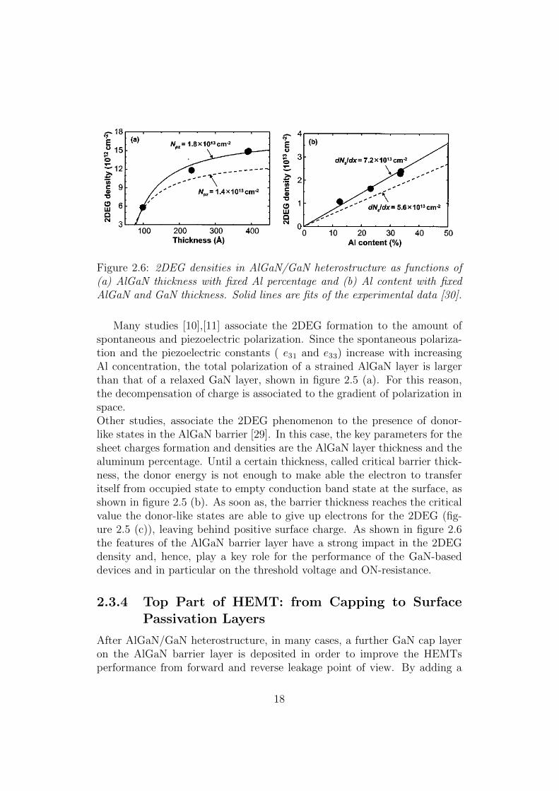
Figure 2.6: 2DEG densities in AlGaN/GaN heterostructure as functions of(a) AlGaN thickness with fixed Al percentage and (b) Al content with fixedAlGaN and GaN thickness. Solid lines are fits of the experimental data [30].
Many studies [10],[11] associate the 2DEG formation to the amount ofspontaneous and piezoelectric polarization. Since the spontaneous polariza-tion and the piezoelectric constants ( e31 and e33) increase with increasingAl concentration, the total polarization of a strained AlGaN layer is largerthan that of a relaxed GaN layer, shown in figure 2.5 (a). For this reason,the decompensation of charge is associated to the gradient of polarization inspace.Other studies, associate the 2DEG phenomenon to the presence of donor-like states in the AlGaN barrier [29]. In this case, the key parameters for thesheet charges formation and densities are the AlGaN layer thickness and thealuminum percentage. Until a certain thickness, called critical barrier thick-ness, the donor energy is not enough to make able the electron to transferitself from occupied state to empty conduction band state at the surface, asshown in figure 2.5 (b). As soon as, the barrier thickness reaches the criticalvalue the donor-like states are able to give up electrons for the 2DEG (fig-ure 2.5 (c)), leaving behind positive surface charge. As shown in figure 2.6the features of the AlGaN barrier layer have a strong impact in the 2DEGdensity and, hence, play a key role for the performance of the GaN-baseddevices and in particular on the threshold voltage and ON-resistance.
2.3.4 Top Part of HEMT: from Capping to SurfacePassivation Layers
After AlGaN/GaN heterostructure, in many cases, a further GaN cap layeron the AlGaN barrier layer is deposited in order to improve the HEMTsperformance from forward and reverse leakage point of view. By adding a
18
thin cap layer of GaN, the piezoelectric effect is exploited in order to increasethe Schottky barrier height and, therefore, to improve the gate leakage [31].
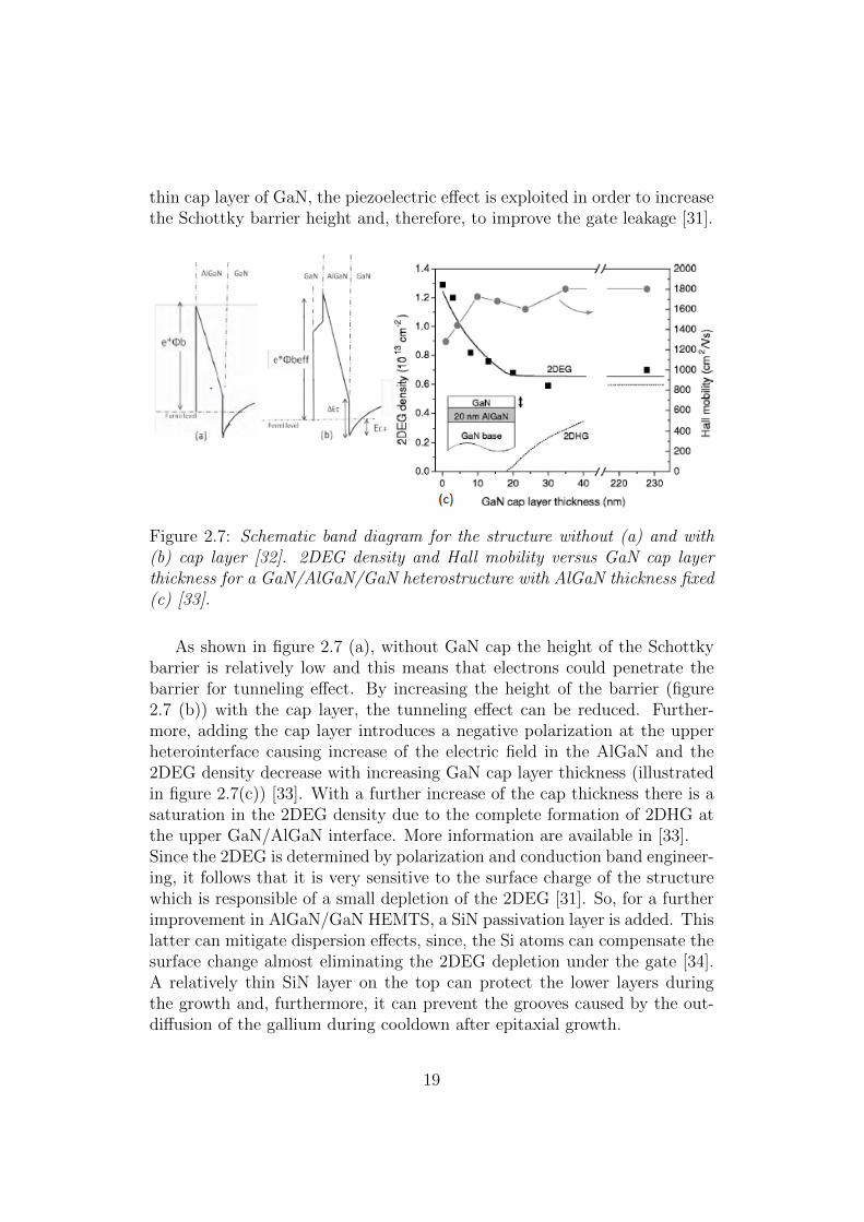
Figure 2.7: Schematic band diagram for the structure without (a) and with(b) cap layer [32]. 2DEG density and Hall mobility versus GaN cap layerthickness for a GaN/AlGaN/GaN heterostructure with AlGaN thickness fixed(c) [33].
As shown in figure 2.7 (a), without GaN cap the height of the Schottkybarrier is relatively low and this means that electrons could penetrate thebarrier for tunneling effect. By increasing the height of the barrier (figure2.7 (b)) with the cap layer, the tunneling effect can be reduced. Further-more, adding the cap layer introduces a negative polarization at the upperheterointerface causing increase of the electric field in the AlGaN and the2DEG density decrease with increasing GaN cap layer thickness (illustratedin figure 2.7(c)) [33]. With a further increase of the cap thickness there is asaturation in the 2DEG density due to the complete formation of 2DHG atthe upper GaN/AlGaN interface. More information are available in [33].Since the 2DEG is determined by polarization and conduction band engineer-ing, it follows that it is very sensitive to the surface charge of the structurewhich is responsible of a small depletion of the 2DEG [31]. So, for a furtherimprovement in AlGaN/GaN HEMTS, a SiN passivation layer is added. Thislatter can mitigate dispersion effects, since, the Si atoms can compensate thesurface change almost eliminating the 2DEG depletion under the gate [34].A relatively thin SiN layer on the top can protect the lower layers duringthe growth and, furthermore, it can prevent the grooves caused by the out-diffusion of the gallium during cooldown after epitaxial growth.
19

The SiN passivation and the GaN cap are used only for depletion-mode de-vices that will be discussed in the following section.
2.4 Lateral GaN Devices for Power Applica-
tion
In the previous section, the layer-by-layer description of the HEMTs hasbeen interrupted because the top part of the devices depends on the variousdevice designs and operation modes. One of the bigger issue of the GaN/Al-GaN devices, with the structure previously described, is that the 2DEG ispresent also without bias and it leads to have normally-ON devices, alsocalled depletion-mode (D-mode) devices. However, in the case of power ap-plications, it is always preferable to have normally-OFF (enhancement-mode)devices for the following reasons:
• safety: the normally-on device is always turned on;
• power consumption: to turn off the normally-on device it is necessaryto apply negative gate voltages;
• costs: driver mature technology already exists for normally-OFF silicon-based MOSFET and it can be expensive to invest money in researchfor new drivers.
Today, the most adopted and commercially available solutions for a normally-OFF GaN devices are: (1) using a cascode configuration by combining alow-voltage Si-MOSFET with a high-voltage D-mode GaN HEMT and (2)E-mode HV GaN HEMT by changing the design of the device.
2.4.1 Cascode Configuration: GaN + Si
One approach to achieve normally-OFF operation for GaN device is thecombination of a high-voltage D-mode GaN HEMT with a low-voltage Si-MOSFET (figure 2.8)[35]. When the Si-FET is turned on by the driversystem, VGS of the HV HEMT is slightly negative and , therefore, the D-mode GaN device is also turned on since it has a high negative thresholdvoltage. When the Si-FET is turned off by the drivers its VDS is really highand, consequently, the VGS of the HV HEMT is sufficiently negative to turnit off, sustaining a high voltage. The advantage of this technique is to usea reliable driver for MOSFET already available on the market without anyneed to redesign another one. Another advantage is that the high OFF-state
20
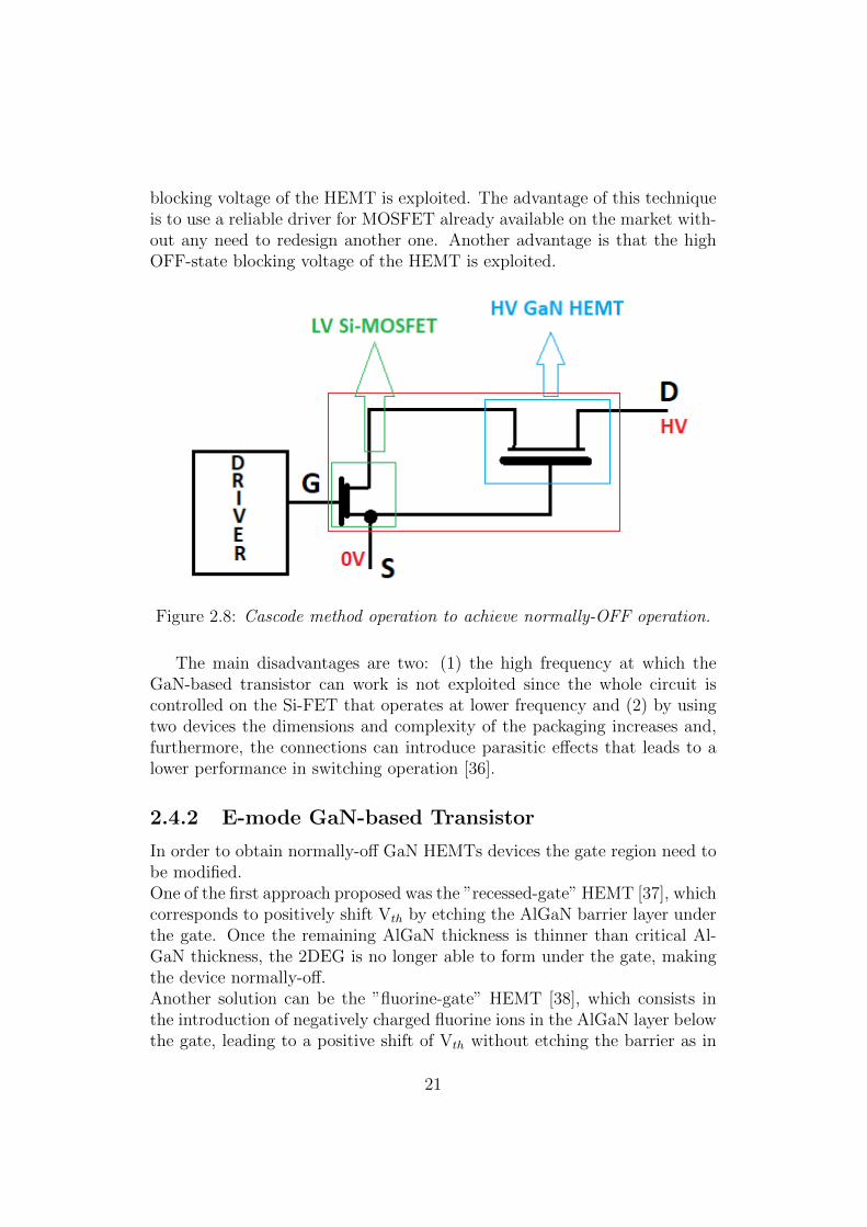
blocking voltage of the HEMT is exploited. The advantage of this techniqueis to use a reliable driver for MOSFET already available on the market with-out any need to redesign another one. Another advantage is that the highOFF-state blocking voltage of the HEMT is exploited.
Figure 2.8: Cascode method operation to achieve normally-OFF operation.
The main disadvantages are two: (1) the high frequency at which theGaN-based transistor can work is not exploited since the whole circuit iscontrolled on the Si-FET that operates at lower frequency and (2) by usingtwo devices the dimensions and complexity of the packaging increases and,furthermore, the connections can introduce parasitic effects that leads to alower performance in switching operation [36].
2.4.2 E-mode GaN-based Transistor
In order to obtain normally-off GaN HEMTs devices the gate region need tobe modified.One of the first approach proposed was the ”recessed-gate” HEMT [37], whichcorresponds to positively shift Vth by etching the AlGaN barrier layer underthe gate. Once the remaining AlGaN thickness is thinner than critical Al-GaN thickness, the 2DEG is no longer able to form under the gate, makingthe device normally-off.Another solution can be the ”fluorine-gate” HEMT [38], which consists inthe introduction of negatively charged fluorine ions in the AlGaN layer belowthe gate, leading to a positive shift of Vth without etching the barrier as in
21

the ”recessed-gate” technique.It is possible to obtain normally-off HEMTs also combing the two approachesjust described [39]. All these solutions have shown to be good from the pointof view of the gate leakage in both reverse and forward bias but there aredifficulties regarding the precision in AlGaN etching and in the right amountof fluorine implanted since they both play a key role in the threshold voltageshift.The most used approaches for normally-off GaN-based HEMTs are the ”p-GaN gate” and the ”recessed gate hybrid MISHEMT” discussed in the fol-lowing subsections.
p-GaN gate HEMT
Interposing a layer of p-GaN between the gate metal and the AlGaN barrier(figure 2.9 (a)) it is possible to deplete the 2DEG under the gate leadingthe GaN-based HEMTs to a normally-off operation as a result of raising theGaN conduction band in the channel above the Fermi level, due to a deple-tion effect of a PN junction. In this scenario the features of the AlGaN andp-GaN layer or the kind of metal gate play an important role for an efficientthreshold voltage positive shift.As already discussed in the subsection 2.3.3, ns increases with the AlGaNbarrier thickness and Al concentration, leading to a lower RON but, as re-ported in [40], a lower Vth is attained due to an inefficient depletion of the2DEG at zero bias. As a result, it is important to find the right trade offbetween the ON-resistance and the threshold voltage. For GaN the p-typedopant is the Magnesium and the key parameter to improve Vth is the Mgelectrical activation and out-diffusion that strongly depend on the growthparameters and annealing conditions [41].Many works report about the importance of the metal work-function on thethreshold voltage and gate leakage. In [42] Vth between 1.7V and 2.1V havedemonstrate with the gate metal made by Ni/Au or Ti/Au, while, it hasbeen reported a threshold voltage around 2.1V with the Schottky gate con-tact, instead of an Ohmic contac, made of TiN [41] or WSiN [43]. This latterworks showed also that the gate leakage current can be reduced. As resultthere is a metal/p-GaN Schottky diode in series with a p-GaN/AlGaN/n-GaN junction 2.9 (b). The gate leakage is reduced since under positive gatevoltages the metal/p-GaN diode is reverse-biased blocking the current and,similarly acts the p-GaN/n-GaN/AlGaN under negative gate bias.Despite the reliability issues still under investigation, the normally-off HEMTwith the p-GaN gate is still the only commercially GaN-based device forpower applications [44], [45] and [46].
22
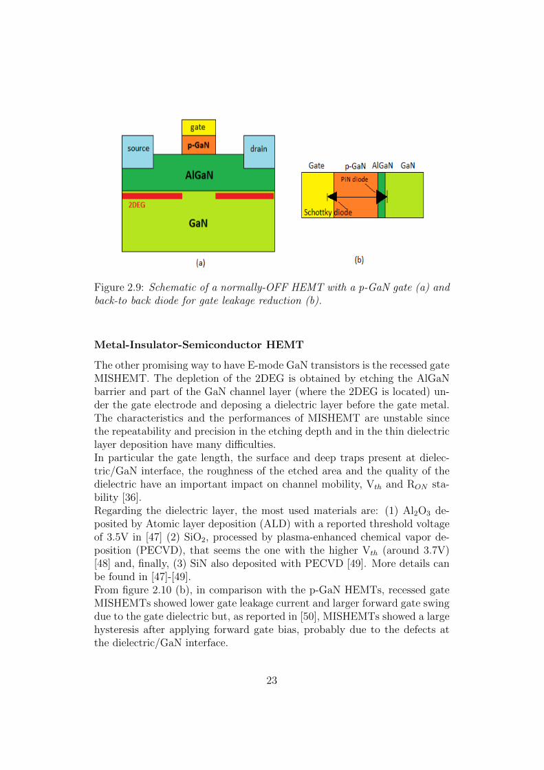
Figure 2.9: Schematic of a normally-OFF HEMT with a p-GaN gate (a) andback-to back diode for gate leakage reduction (b).
Metal-Insulator-Semiconductor HEMT
The other promising way to have E-mode GaN transistors is the recessed gateMISHEMT. The depletion of the 2DEG is obtained by etching the AlGaNbarrier and part of the GaN channel layer (where the 2DEG is located) un-der the gate electrode and deposing a dielectric layer before the gate metal.The characteristics and the performances of MISHEMT are unstable sincethe repeatability and precision in the etching depth and in the thin dielectriclayer deposition have many difficulties.In particular the gate length, the surface and deep traps present at dielec-tric/GaN interface, the roughness of the etched area and the quality of thedielectric have an important impact on channel mobility, Vth and RON sta-bility [36].Regarding the dielectric layer, the most used materials are: (1) Al2O3 de-posited by Atomic layer deposition (ALD) with a reported threshold voltageof 3.5V in [47] (2) SiO2, processed by plasma-enhanced chemical vapor de-position (PECVD), that seems the one with the higher Vth (around 3.7V)[48] and, finally, (3) SiN also deposited with PECVD [49]. More details canbe found in [47]-[49].From figure 2.10 (b), in comparison with the p-GaN HEMTs, recessed gateMISHEMTs showed lower gate leakage current and larger forward gate swingdue to the gate dielectric but, as reported in [50], MISHEMTs showed a largehysteresis after applying forward gate bias, probably due to the defects atthe dielectric/GaN interface.
23
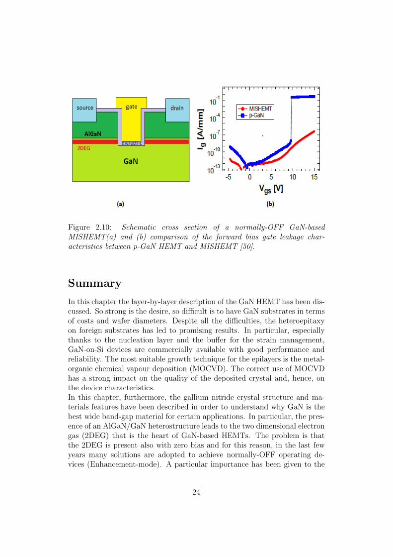
Figure 2.10: Schematic cross section of a normally-OFF GaN-basedMISHEMT(a) and (b) comparison of the forward bias gate leakage char-acteristics between p-GaN HEMT and MISHEMT [50].
Summary
In this chapter the layer-by-layer description of the GaN HEMT has been dis-cussed. So strong is the desire, so difficult is to have GaN substrates in termsof costs and wafer diameters. Despite all the difficulties, the heteroepitaxyon foreign substrates has led to promising results. In particular, especiallythanks to the nucleation layer and the buffer for the strain management,GaN-on-Si devices are commercially available with good performance andreliability. The most suitable growth technique for the epilayers is the metal-organic chemical vapour deposition (MOCVD). The correct use of MOCVDhas a strong impact on the quality of the deposited crystal and, hence, onthe device characteristics.In this chapter, furthermore, the gallium nitride crystal structure and ma-terials features have been described in order to understand why GaN is thebest wide band-gap material for certain applications. In particular, the pres-ence of an AlGaN/GaN heterostructure leads to the two dimensional electrongas (2DEG) that is the heart of GaN-based HEMTs. The problem is thatthe 2DEG is present also with zero bias and for this reason, in the last fewyears many solutions are adopted to achieve normally-OFF operating de-vices (Enhancement-mode). A particular importance has been given to the
24

p-GaN gate HEMTs and recessed gate MISHEMTs, though, the p-GaN gatesolution is the only one commercially available since MISHEMTs have someproblem in terms of stability and repeatability in the process.
25
Chapter 3
GaN Reliability Issues
In addition to excellent performance at reduced cost, a semiconductor powerdevice must guarantee a good level of reliability before making it available onthe electronic market. Despite GaN power transistors demonstrated impres-sive performance at comparable costs with respect to Si-counterparts, thelong-term reliability is still an issue not to be underestimated. GaN-basedHEMTs are usually adopted in switching power applications, where theirstate is continuously switched, at relatively high frequencies, between highvoltage off-state and high current on-state operation. In such conditions,devices can be subjected to different kinds of degradation mechanisms lim-iting their long-term reliability. Furthermore, during the switching phasesthe devices might be simultaneously subjected, for a short period of time,to both high-drain voltage and current. This regime is called semi-on-stateoperation and can lead to additional degradation mechanisms.In general, the time-dependent degradation of GaN-based transistors may betriggered by many factors,, widely classified in [51] as follow:
1. Material origin: crystalline defects and lack of uniformity in the de-posited epilayer;
2. Metallurgy: ohmic contact and passivation degradation, hydrogen con-tamination, etc.;
3. Electrical behavior: reduction in drain current (current collapse), in-creasing in power consumption (power drift), breakdown walkout, etc.;
Beside the aforementioned failure mechanisms, this chapter will focuswith particular attention on trapping defects and self-heating problems.The key to better understand how reliable a device is, or which failure mech-anism leads to the degradation, resides in the thermo-electrical stress andcharacterization of the devices.
26
3.1 Trapping effects
Trapping effects are the main cause of power GaN HEMTs degradation. Theterm traps refers to the defects deriving as a consequence of crystal imper-fections, threading dislocation or impurities, etc. The traps can introduceenergy states in the bandgap of the semiconductor. These states can be: i)acceptor-like, i.e neutral when empty and negatively charged when occupied;ii) donor-like, i.e neutral when empty and positively charged when occupied.[52]
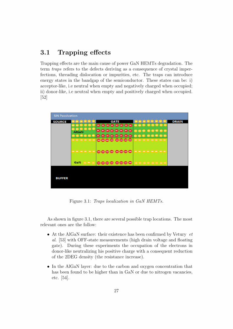
Figure 3.1: Traps localization in GaN HEMTs.
As shown in figure 3.1, there are several possible trap locations. The mostrelevant ones are the follow:
• At the AlGaN surface: their existence has been confirmed by Vetury etal. [53] with OFF-state measurements (high drain voltage and floatinggate). During these experiments the occupation of the electrons indonor-like neutralizing his positive charge with a consequent reductionof the 2DEG density (the resistance increase).
• In the AlGaN layer: due to the carbon and oxygen concentration thathas been found to be higher than in GaN or due to nitrogen vacancies,etc. [54].
27

• In the GaN layer: as seen in the previous chapter, a carbon doped GaNbuffer is required to suppress the current leakage. Still, the dopingintroduces acceptor-like impurities [52], [55].
• At the interfaces between layers of different materials: these traps canbe related to threading dislocation caused by lattice constants and ther-mal expansion coefficients between adopted epi-materials [56], [57].
• In the buffer (not shown in Fig. 3.1): this kind of traps are localizedin the stack between the GaN channel layer and the substrate due tolattice mismatch between the various epilayer made of different mate-rials.
To determine a specific degradation mechanism, it is necessary to understandhow the traps behave and what energy levels they are related to, where theyare physically localized and what trapping/de-trapping time constants dothey have. To do this, various trap characterization experiments, such asCurrent-Transient measurements [58], frequency dependent capacitance andconductance measurements [59] and capacitance-voltage (C-V) have beenemployed.Based on their localization, each kind of trap can impact a different param-eter. In particular, the traps localized in the region under the gate (in redin figure 3.1) have a dominant impact on the threshold voltage, while allthe other impurities (in yellow in figure 3.1) could lead to a change in thetransconductance due to resistivity increase of the gate-drain and gate-sourceaccess regions [60].
3.2 On-State Degradation Mechanisms
In on-state condition the GaN devices are submitted to a low drain volt-age, but normally-off devices operate with positives gate biases that lead tofurther degradation mechanisms. The reliability issues for MISHEMTs andp-GaN gate HEMTs are different because of the different gate stack.As already said in the section 2.4, MISHEMTs suffer of threshold voltageinstability due to defect states at the dielectric/AlGaN interface. Lagger etal. [61] explained Vth degradation with a schematic band diagram (Fig. 3.2).In particular, by increasing the gate bias (VG), the electrons barrier heightbetween 2DEG and dielectric/AlGaN interface decreases, favoring electroninjection. A further increase in VG pushes the AlGaN conduction band (Fig.3.2(c)) at the interface with the dielectric below the Fermi level, with a con-sequent formation of a second channel. As a result, the Vth shifts depends
28
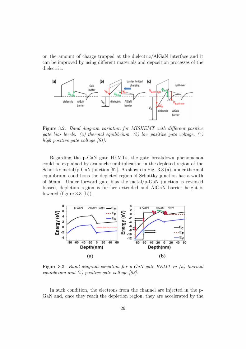
on the amount of charge trapped at the dielectric/AlGaN interface and itcan be improved by using different materials and deposition processes of thedielectric.
Figure 3.2: Band diagram variation for MISHEMT with different positivegate bias levels: (a) thermal equilibrium, (b) low positive gate voltage, (c)high positive gate voltage [61].
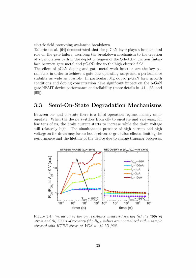
Regarding the p-GaN gate HEMTs, the gate breakdown phenomenoncould be explained by avalanche multiplication in the depleted region of theSchottky metal/p-GaN junction [62]. As shown in Fig. 3.3 (a), under thermalequilibrium conditions the depleted region of Schottky junction has a widthof 50nm. Under forward gate bias the metal/p-GaN junction is reversedbiased, depletion region is further extended and AlGaN barrier height islowered (figure 3.3 (b)).
Figure 3.3: Band diagram variation for p-GaN gate HEMT in (a) thermalequilibrium and (b) positive gate voltage [63].
In such condition, the electrons from the channel are injected in the p-GaN and, once they reach the depletion region, they are accelerated by the
29
electric field promoting avalanche breakdown.Tallarico et al. [64] demonstrated that the p-GaN layer plays a fundamentalrole on the gate failure, ascribing the breakdown mechanism to the creationof a percolation path in the depletion region of the Schottky junction (inter-face between gate metal and pGaN) due to the high electric field.The effect of pGaN doping and gate metal work function are the key pa-rameters in order to achieve a gate bias operating range and a performancestability as wide as possible. In particular, Mg doped p-GaN layer growthconditions and doping concentration have significant impact on the p-GaNgate HEMT device performance and reliability (more details in [41], [65] and[66]).
3.3 Semi-On-State Degradation Mechanisms
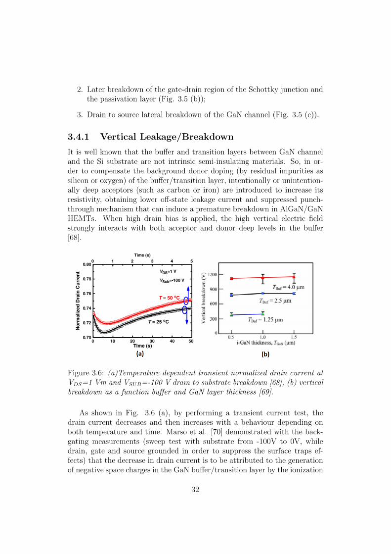
Between on- and off-state there is a third operation regime, namely semi-on-state. When the device switches from off- to on-state and viceversa, forfew tens of ns, the drain current starts to increase while the drain voltagestill relatively high. The simultaneous presence of high current and highvoltage on the drain may favour hot electrons degradation effects, limiting theperformance and the lifetime of the device due to charge trapping processes.
Figure 3.4: Variation of the on resistance measured during (a) the 200s ofstress and (b) 5000s of recovery (the RON values are normalized with a samplestressed with HTRB stress at VGS = -10 V) [62].
30

In particular, is such regime, electrons injected from the source are ac-celerated by the high longitudinal electric field toward the drain, acquiringenough kinetic energy to create new defects and/or to be trapped in pre-existing ones, [67]. The most affected parameter is the on-resistance, and inorder to investigate the hot electrons role in the degradation, high temper-ature source current (HTSC) stress tests are performed. Here, the devicesare stressed for a long period of time with constant current injection fromthe source and with a high drain voltage. In figure 3.4 (a), it is possible tonotice that the RON increases with both the current and time, but, on theother hand, the hot electrons induced degradation is recoverable as resultof trapping in the gate-drain access region. By increasing the temperature,the on-resistance degradation decreases because the mean energy of the hotelectrons is reduced by the scattering with the lattice. Still, these scatteringcould produce unrecoverable damage [62].
3.4 Off-State Degradation Mechanisms
During Off-state operation, the devices are submitted to a high drain voltagehaving their bulk, source and gate contacts grounded.
Figure 3.5: Different off-state breakdown mechanisms namely: (a) drain tosubstrate breakdown, (b) drain to gate breakdown and (c) drain to sourcebreakdown
This operation mode can lead to an unrecoverable breakdown that istime-dependent, a situation that also occurs at drain voltages lower thanthe breakdown voltage evaluated by a dc sweep. The off-state breakdownmechanism can be summarized in:
1. Vertical drain to substrate breakdown of the buffer (Fig. 3.5 (a));
31
2. Later breakdown of the gate-drain region of the Schottky junction andthe passivation layer (Fig. 3.5 (b));
3. Drain to source lateral breakdown of the GaN channel (Fig. 3.5 (c)).
3.4.1 Vertical Leakage/Breakdown
It is well known that the buffer and transition layers between GaN channeland the Si substrate are not intrinsic semi-insulating materials. So, in or-der to compensate the background donor doping (by residual impurities assilicon or oxygen) of the buffer/transition layer, intentionally or unintention-ally deep acceptors (such as carbon or iron) are introduced to increase itsresistivity, obtaining lower off-state leakage current and suppressed punch-through mechanism that can induce a premature breakdown in AlGaN/GaNHEMTs. When high drain bias is applied, the high vertical electric fieldstrongly interacts with both acceptor and donor deep levels in the buffer[68].
Figure 3.6: (a)Temperature dependent transient normalized drain current atVDS=1 Vm and VSUB=-100 V drain to substrate breakdown [68], (b) verticalbreakdown as a function buffer and GaN layer thickness [69].
As shown in Fig. 3.6 (a), by performing a transient current test, thedrain current decreases and then increases with a behaviour depending onboth temperature and time. Marso et al. [70] demonstrated with the back-gating measurements (sweep test with substrate from -100V to 0V, whiledrain, gate and source grounded in order to suppress the surface traps ef-fects) that the decrease in drain current is to be attributed to the generationof negative space charges in the GaN buffer/transition layer by the ionization
32

of acceptor traps, which depletes the 2DEG, and that the increase in draincurrent is caused by the ionization of donor traps, which generates positivespace charges. Fig. 3.6 (b) shows the trend of the vertical breakdown byvarying the buffer thickness (TBuf ) and the GaN layer thickness (TGaN). Inparticular, it can be seen that the breakdown voltage is slightly affected byTGaN , while TBuf plays a more important role [69].Many studies have investigated the responsible factors of the vertical con-duction, proposing some solutions such as the use of a highly resistive siliconsubstrate [71] or the insertion of a p-type region [72] due to the fact that thevoltage drop on the GaN buffer is mitigated by the partial depletion of thesubstrate.
3.4.2 Lateral Breakdown in the Gate-Drain Region
The other region affected by degradation/breakdown is the one between drainand gate. In particular, the breakdown can occur at the Schottky junctionand/or at the passivation layer, and it is caused by the high electric fielddue to high voltage between gate and drain, VGD. Regarding the Schottkyjunction, the real cause is a high peak of the electric field at the gate edgeon the drain side, as it can trigger the following mechanisms:
• Inverse piezoelectric effect: as it is well known, the AlGaN barrier layeris subject to a tensile stress due to the lattice mismatch with the GaNchannel layer. This can produce crystallographic defects resulting inthe degradation of the electrical characteristics due to trapping/de-trapping effects. Ancona et al. [73] demonstrated with an electrome-chanical analysis that the piezoelectric effect alone is not sufficient togenerate a crack in the AlGaN layer, but the combination of the highelectric field, gate leakage current and high temperature together leadto the breakage. The role of the AlGaN barrier properties is very im-portant and by reducing the Al content the mechanical stress with theGaN layer is reduced, though, the performance (such as the RON sincethe 2DEG has a lower density) will be worse.
• Electrochemical degradation: by etching the passivation and the met-allization from the device (without damaging the AlGaN or the GaNsurface) Makaram et al. [74] showed the presence of grooves and parti-cles. They also demonstrated that with the increase of the electric fieldin off-state conditions, the number of the particles and the depth of thegrooves increased at the drain-side of the gate edge. These phenomenaare related to an electrochemical reaction consisting in the oxidationof GaN or AlGaN, with formation of Ga2O3 and Al2O3 [75]. The main
33
issue is that the grooves and the particles can charge the device sur-face, forming a virtual gate responsible of drain current collapse andgate leakage current increase [76].
• Percolation processes: high electric field is also responsible for an in-crease in the amount of defects in the AlGaN barrier layer (demon-strated by electroluminescence measurements [77]). This can create apercolation multistep tunnelling path. The number of defects creatinga percolation path is voltage and time dependent, as they lead to anincrease of the gate leakage current (until the permanent breakdown)and a shift of I-V curves measured after constant voltage stress [78].
It emerges that the main issues for the gate-drain region are the highelectric field peaks and the impurities in the epilayers. Both of them mayproduce current collapse, which consists in a drastic reduction of the draincurrent (ID) after the application of a high drain voltage (VD) [79]. Thecurrent collapse is caused by acceptor-like traps in both AlGaN/GaN layersand the passivation/AlGaN interface: this leads to trapping mechanism ofthe 2DEG electrons accelerated by the high electric field [52].
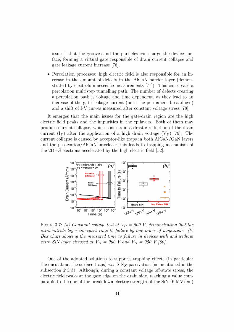
Figure 3.7: (a) Constant voltage test at VD = 900 V, demonstrating that theextra nitride layer increases time to failure by one order of magnitude. (b)Box chart showing the measured time to failure in devices with and withoutextra SiN layer stressed at VD = 900 V and VD = 950 V [80].
One of the adopted solutions to suppress trapping effects (in particularthe ones about the surface traps) was SiNX passivation (as mentioned in thesubsection 2.3.4 ). Although, during a constant voltage off-state stress, theelectric field peaks at the gate edge on the drain side, reaching a value com-parable to the one of the breakdown electric strength of the SiN (6 MV/cm)
34

[80]. In particular, in [80], an improvement has been found by adding anextra SiN layer above the already present one. The electric field peak hasbeen reduced, resulting in one order of magnitude increase of the time tofailure/breakdown with respect to the devices without the extra SiN layer,shown in Fig. 3.7.Another way to increase the breakdown voltage is by reducing the electricfield (close to gate edge) with the adoption of the field plates. As shown inFig. 3.8, this approach consists in depositing three metal layers, two linkedto the source and one to the gate, all of them separated by oxide layers. Inparticular, the longer the field plates, the lower the electric fields. However,it is worth noting that a too long field plate (e.g. S-FP2 in Fig. 1.5) couldlead to a lower breakdown voltage due to short distance between field plateand drain contact. As a result, the right trade-off must be achieved.
Figure 3.8: Cross-section of a GaN HEMT with double source field plates(S-FP1 and S-FP2) and single gate field plate (G-FP).
3.4.3 Lateral Breakdown between Source and Drain
Finally, the last breakdown mechanism with regards to the off-state condi-tion, is the one involving th GaN channel layer. This breakdown is due toan increase in the drain-source leakage current, linked to the punch-througheffects. If the region of the GaN channel under the gate is not well depleted,the high drain voltage allows a current flow through the GaN layer in a deeperposition respect to the AlGaN/GaN interface and strongly depends on thegate length [81]. As shown in Fig. 3.9 (a) , the higher the negative VGS, thehigher the punch-through voltage,, since the GaN channel under the gate is
35
more depleted in the vertical direction (towards the buffer).
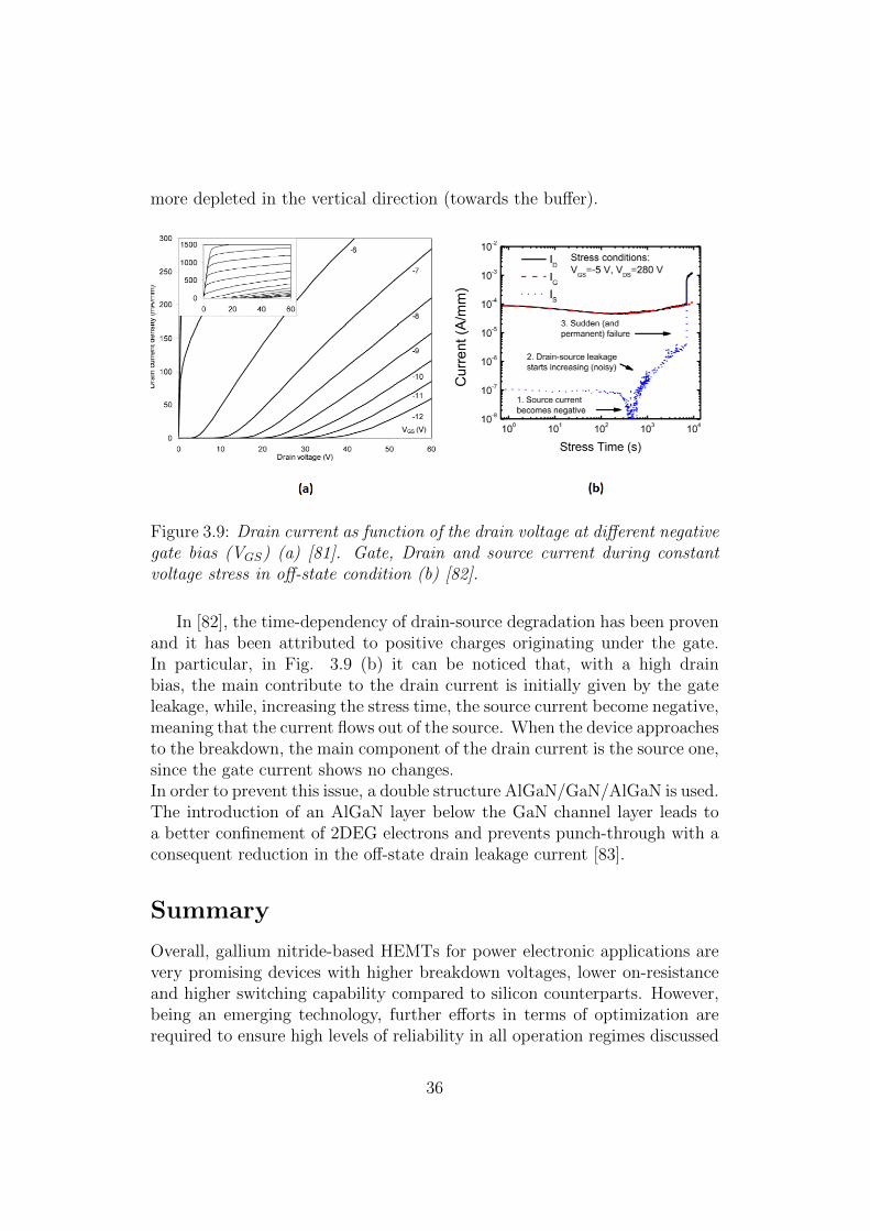
Figure 3.9: Drain current as function of the drain voltage at different negativegate bias (VGS) (a) [81]. Gate, Drain and source current during constantvoltage stress in off-state condition (b) [82].
In [82], the time-dependency of drain-source degradation has been provenand it has been attributed to positive charges originating under the gate.In particular, in Fig. 3.9 (b) it can be noticed that, with a high drainbias, the main contribute to the drain current is initially given by the gateleakage, while, increasing the stress time, the source current become negative,meaning that the current flows out of the source. When the device approachesto the breakdown, the main component of the drain current is the source one,since the gate current shows no changes.In order to prevent this issue, a double structure AlGaN/GaN/AlGaN is used.The introduction of an AlGaN layer below the GaN channel layer leads toa better confinement of 2DEG electrons and prevents punch-through with aconsequent reduction in the off-state drain leakage current [83].
Summary
Overall, gallium nitride-based HEMTs for power electronic applications arevery promising devices with higher breakdown voltages, lower on-resistanceand higher switching capability compared to silicon counterparts. However,being an emerging technology, further efforts in terms of optimization arerequired to ensure high levels of reliability in all operation regimes discussed
36

in this chapter, i.e. (1) on-state, (2) semi-on-state, (3) off-state. The nextchapter reports an experimental activity aimed at investigating the off-statereliability of power GaN HEMTs with p-type gate fabricated on 200 mmsilicon substrates by imec.
37

Chapter 4
Investigation of the Off-StateReliability on 200V pGaNHEMTs
In this chapter an Off-state reliability study is presented performed on 200V p-GaN HEMTs featuring different structural configurations summarizedin section 1.1.1. In particular, time-dependent dielectric breakdown andhard breakdown experimental tests have been performed in combination withTCAD simulations. Thanks to this approach, the root causes limiting theoff-state device reliability have been identified, highlighting the role and theimportance of structural parameters, which are fundamental for guiding de-vice optimization.
4.1 Experimental Details
Off-state electrical stress and measurements have been carried out by meansof a MPI-TS2000-HP probe station connected to KEYSIGHT B1505A pa-rameter analyser equipped with high power, high voltage and ground sourcemeasure units (SMUs). In particular, the devices under test are connectedas follows:
• Source contact: connected to high power SMU (HPSMU1);
• Drain contact: connected to high voltage SMU (HVSMU);
• Gate contact: connected to high power SMU (HPSMU2);
• Substrate contact: connected to ground SMU (GNDSMU);
38
During Off-state stress, the gate, source and bulk contacts are forced to 0 Vwhile, the drain voltage is sweeped up to stress voltage and/or breakdownvoltage. All contacts currents are monitored. Usually, accelerated stresstests are performed at 150 oC but, in this case, a temperature of 210 oC hasbeen adopted to limit the stress voltage (< 500 V) and time-to-failure (< 105
s). Devices with different geometry parameters such as gate-drain distance(LGD) and the field plates lengths have been adopted. The role of the AlGaNbarrier thickness (TAlGaN), Al content, and GaN channel thickness (TGaN)on the off-state degradation has been also investigated.
4.1.1 Device Under Test
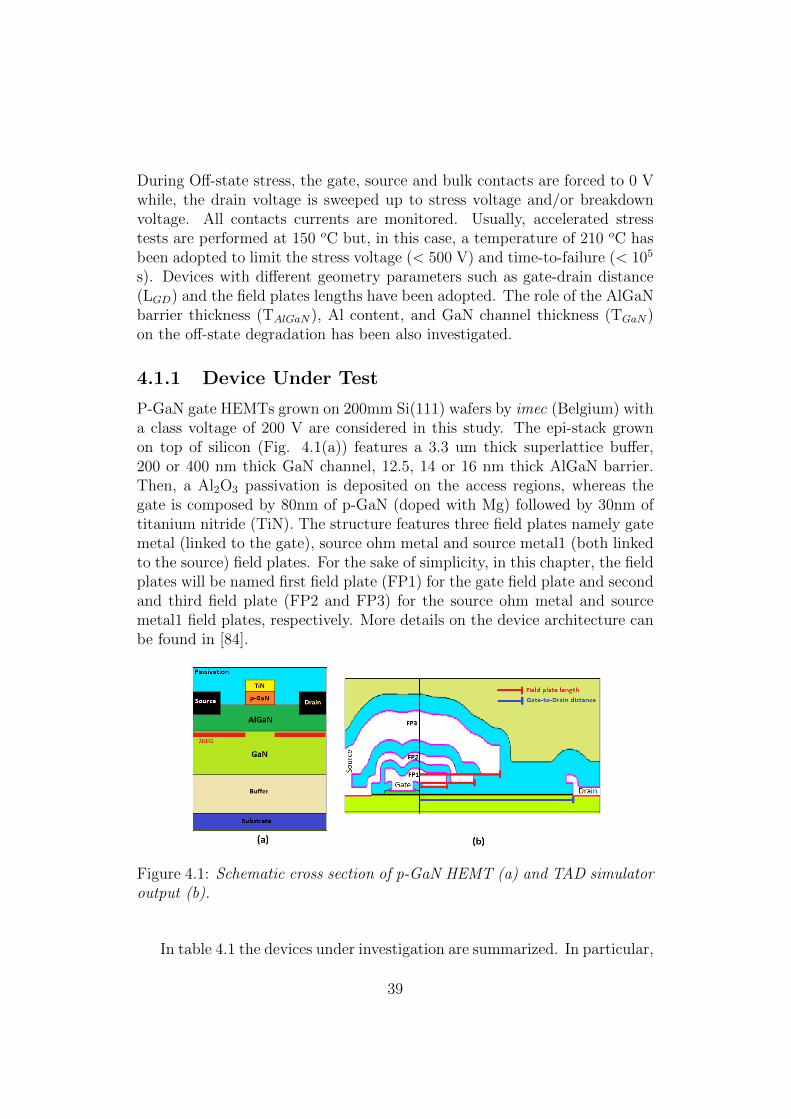
P-GaN gate HEMTs grown on 200mm Si(111) wafers by imec (Belgium) witha class voltage of 200 V are considered in this study. The epi-stack grownon top of silicon (Fig. 4.1(a)) features a 3.3 um thick superlattice buffer,200 or 400 nm thick GaN channel, 12.5, 14 or 16 nm thick AlGaN barrier.Then, a Al2O3 passivation is deposited on the access regions, whereas thegate is composed by 80nm of p-GaN (doped with Mg) followed by 30nm oftitanium nitride (TiN). The structure features three field plates namely gatemetal (linked to the gate), source ohm metal and source metal1 (both linkedto the source) field plates. For the sake of simplicity, in this chapter, the fieldplates will be named first field plate (FP1) for the gate field plate and secondand third field plate (FP2 and FP3) for the source ohm metal and sourcemetal1 field plates, respectively. More details on the device architecture canbe found in [84].
Figure 4.1: Schematic cross section of p-GaN HEMT (a) and TAD simulatoroutput (b).
In table 4.1 the devices under investigation are summarized. In particular,
39
each device differs for gate-drain distance and field plate length configuration.
Device name LGD (µm) FP1 (µm) FP2 (µm) FP3 (µm)Device1 3 0.35 0.65 1Device2 4 0.65 1.35 2Device3 5 1 2 3Device4 6 1 2 3
Table 4.1: Overview of the devices under test.
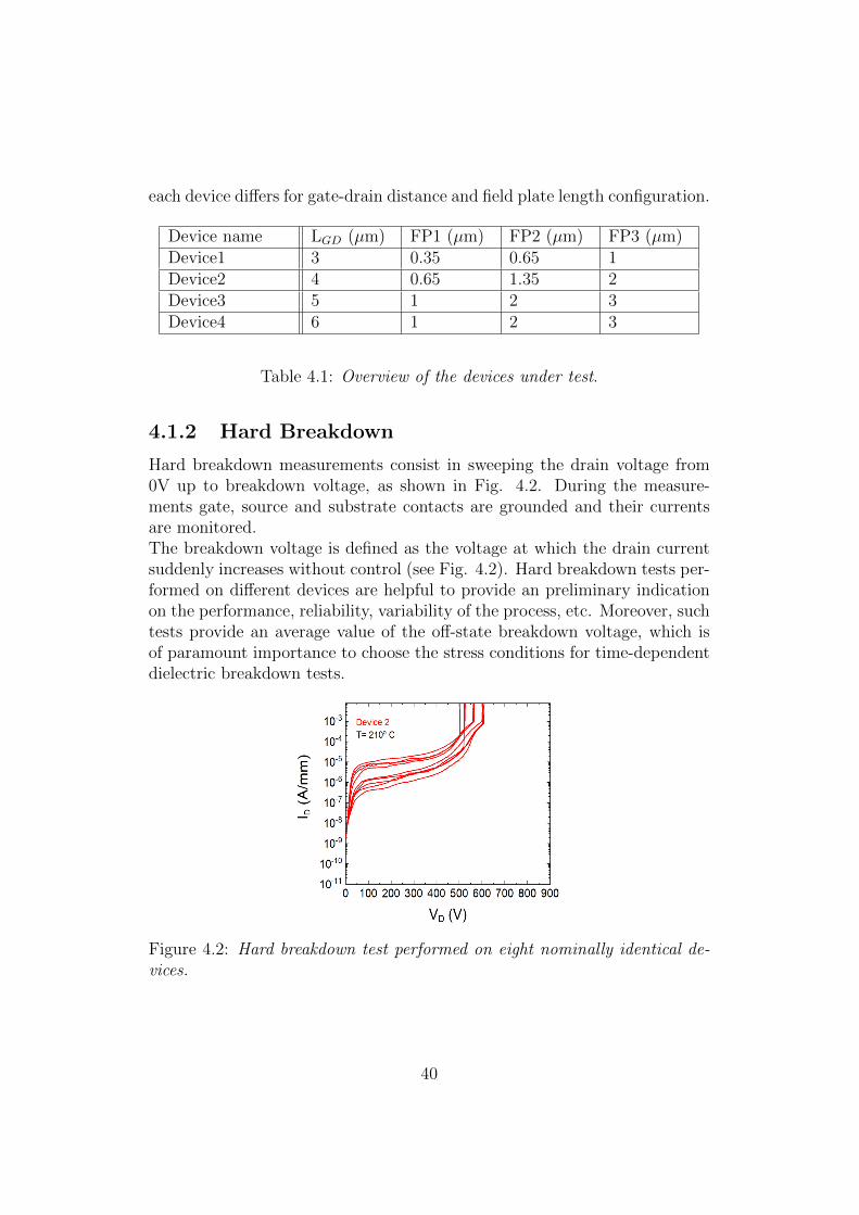
4.1.2 Hard Breakdown
Hard breakdown measurements consist in sweeping the drain voltage from0V up to breakdown voltage, as shown in Fig. 4.2. During the measure-ments gate, source and substrate contacts are grounded and their currentsare monitored.The breakdown voltage is defined as the voltage at which the drain currentsuddenly increases without control (see Fig. 4.2). Hard breakdown tests per-formed on different devices are helpful to provide an preliminary indicationon the performance, reliability, variability of the process, etc. Moreover, suchtests provide an average value of the off-state breakdown voltage, which isof paramount importance to choose the stress conditions for time-dependentdielectric breakdown tests.
Figure 4.2: Hard breakdown test performed on eight nominally identical de-vices.
40
4.1.3 Time-Dependent Dielectric Breakdown (TDDB)
Time-dependent dielectric breakdown has been studied for the first time inthin oxide films [85] and [86], due to their importance in silicon CMOS in-tegrated circuits. Regarding GaN devices, the situation is slightly differentsince the time-dependent breakdown can occur in different regions/materials,i.e. passivation layers (SiO2, AlO2, SiN, etc.), or semiconductor layers (GaN,AlGaN, etc.) [87], [80], [88] . The most commonly used test for the inves-tigation of TDDB behavior is ”constant stress”. Such stress can be appliedin form of constant voltage stress (CVS) or constant current stress (CCS).In the case of CVS test adopted for off-state reliability of GaN devices, avoltage is applied to the drain, while its leakage current is being monitoredup to failure.
Time-to-Breakdown
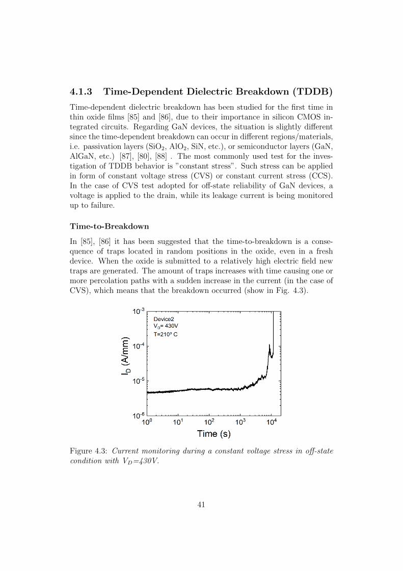
In [85], [86] it has been suggested that the time-to-breakdown is a conse-quence of traps located in random positions in the oxide, even in a freshdevice. When the oxide is submitted to a relatively high electric field newtraps are generated. The amount of traps increases with time causing one ormore percolation paths with a sudden increase in the current (in the case ofCVS), which means that the breakdown occurred (show in Fig. 4.3).
Figure 4.3: Current monitoring during a constant voltage stress in off-statecondition with VD=430V.
41

In the case of a CVS, the time-to-breakdown (tBD), also called time-to-failure (TTF), corresponds to the time when the current (the drain currentin the case illustrated in Fig. 4.3) increase beyond a defined current value.
Statistical Analysis
When TDDB stress is applied on several devices with same geometry, dif-ferent times-to-breakdown occur because of non-ideality of devices, process,etc. Actually, the tBD is a statistical distributed parameter with cumulativefailure distribution function F(t), which can be calculated from a fitting ofthe cumulative distribution of the tBD values. The tBD values in [85], [86]have been shown to be distributed according to Weibull statistic distributionfunction defined as:
F (t) = 1 − exp[−(t− γ
η)β] (4.1)
where β is the shape parameter, η is the scale factor (or the time in whichthe 63.2% of the devices fail) and γ is the time delay. Assuming γ=0 the eq.4.1 can be rewritten as:
ln[−ln(1 − F (t))] = βln(t) − βln(η) (4.2)
The analysis procedure for the TDDB experiments can be summarized asfollow [85], [86]:
1. Extraction of tBD values from the recorded measurements during CVStest (Fig. 4.4(a));
2. Ordering the obtained tBD values from the smallest to the biggest andextraction of F(tBD−i) (Fig. 4.4(b)) by the Bernard formula of themedian ranking approximation:
F (tBD−i) =i− 0.3
n+ 0.4(4.3)
where i is the number of the i-th failed device, and n is the total numberof failed devices;
3. Plot the F(tBD−i) data in a Weibull plot (ln[-ln(1-F(tBD−i))] vs. ln(tBD−i)))and apply a linear fit (Fig. 4.4(c)).
Finally, from the Weibull plot it is possible to extract the value of βand η. The shape parameter β of the Weibull distribution represents theslope of F(t) function and it can give information about the reliability. In
42

particular, β>1 indicates a smaller spread on the data which means that thetime-to-breakdown is induced by a single degradation mechanism (intrinsicbreakdown). When β<1, the presence of different degradation mechanismsor the poor quality of the device process is the root cause for TDDB (extrinsicbreakdown).
Figure 4.4: Example of analysis for a TDDB experiment:(a) tBD values areextracted from the measurements, (b) the obtained tBD values are ordered(from the smallest to the biggest) and then the F(tBD−i) is calculate usingthe Bernard formula. Finally (c) from the plot of ln[-ln(1-F(tBD−i))] vs.ln(tBD−i) the values of η and β can be extrapolated.
The scale factor η strongly depends on the applied voltage and the areaof the devices. Since the percolation paths could be formed randomly inthe device area, a larger area implies a higher failure probability (lower η).Based on TDDB theory,the F(t) of different areas with the same dielectricthickness follows the area scaling law [85]. In particular, the Weibull functionof devices with area A1 (FA1(t)) can be expressed as a function of the thesame F(t) of devices with area A2 (FA2(t)) as follows:
ln[−ln(1 − FA1(t))] = ln(A2
A1
) + ln[−ln(1 − FA2(t))] (4.4)
43

Replacing the Eq. 4.2 in 4.4:
ln(A2
A1
) + βln(t) − βln(η2) = βln(t) − βln(η1) (4.5)
where:
η1 = η2(A2
A1
)1β (4.6)
The area scaling produce a time-shift by (A2/A1)1β of the Weibull plot with
an alignment of the two straight lines only in case of homogenous stressand degradation (same β for the Weibull plots related to A1 and A2). Onthe other hand, if the failure (forming of percolation path) occurs in a verylocalized spot (e.g. at a corner), the area is not responsible of a η shift andthe Eq. 4.6 can not be applied [89].
Lifetime extrapolation
Figure 4.5: Example of lifetime extrapolation:(a) Weibull plot associated withTDDB experiments under 3 different stress condition, (b) lifetime predictionfrom the values of η1, η2 and η3 [89].
As mentioned above, the Weibull parameter η depends on the applied voltage(in the case of CVS), indeed, a larger voltage means a lower value of η.By performing TDDB experiments at different stress conditions (voltage orcurrent) the resulting failure distributions F(t) are parallel to each other(same β) and only shifted by the η factor as shown in Fig. 4.5 (a). Toextrapolate the lifetime it is necessary to plot the different η values versus
44
the stress conditions and, by fitting this relation with an exponential law,it is possible to predict when the 63.2% of the devices fail under a certainoperating voltage (shown in Fig. 4.5 (b)). Additionally, it is possible toextract the time corresponding to the failure of an arbitrary percentage x%and determine the guaranteed operating conditions [89]. Note that the stressconditions are always higher than the operating condition in order to obtainthe failure in a reasonable time.
4.2 Results and Discussion
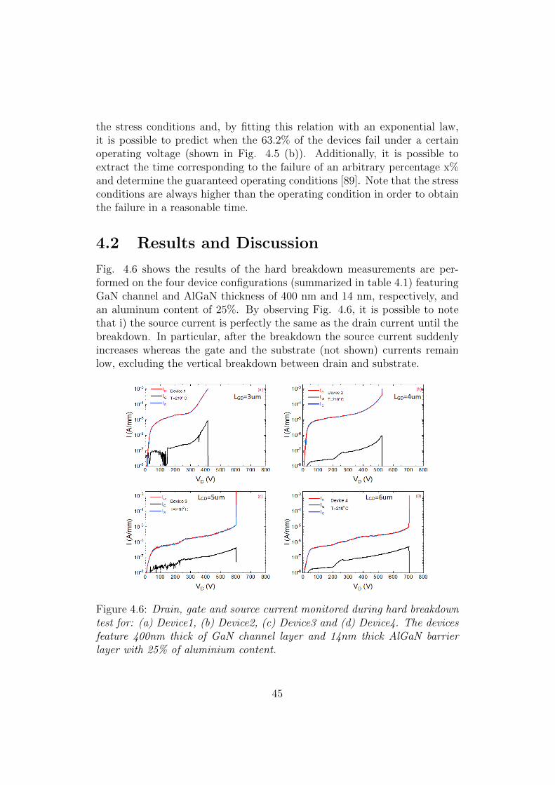
Fig. 4.6 shows the results of the hard breakdown measurements are per-formed on the four device configurations (summarized in table 4.1) featuringGaN channel and AlGaN thickness of 400 nm and 14 nm, respectively, andan aluminum content of 25%. By observing Fig. 4.6, it is possible to notethat i) the source current is perfectly the same as the drain current until thebreakdown. In particular, after the breakdown the source current suddenlyincreases whereas the gate and the substrate (not shown) currents remainlow, excluding the vertical breakdown between drain and substrate.
Figure 4.6: Drain, gate and source current monitored during hard breakdowntest for: (a) Device1, (b) Device2, (c) Device3 and (d) Device4. The devicesfeature 400nm thick of GaN channel layer and 14nm thick AlGaN barrierlayer with 25% of aluminium content.
45
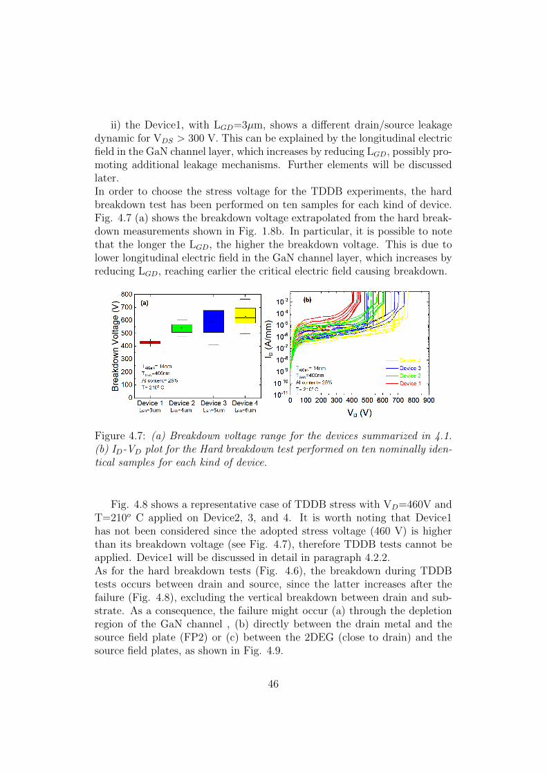
ii) the Device1, with LGD=3µm, shows a different drain/source leakagedynamic for VDS > 300 V. This can be explained by the longitudinal electricfield in the GaN channel layer, which increases by reducing LGD, possibly pro-moting additional leakage mechanisms. Further elements will be discussedlater.In order to choose the stress voltage for the TDDB experiments, the hardbreakdown test has been performed on ten samples for each kind of device.Fig. 4.7 (a) shows the breakdown voltage extrapolated from the hard break-down measurements shown in Fig. 1.8b. In particular, it is possible to notethat the longer the LGD, the higher the breakdown voltage. This is due tolower longitudinal electric field in the GaN channel layer, which increases byreducing LGD, reaching earlier the critical electric field causing breakdown.
Figure 4.7: (a) Breakdown voltage range for the devices summarized in 4.1.(b) ID-VD plot for the Hard breakdown test performed on ten nominally iden-tical samples for each kind of device.
Fig. 4.8 shows a representative case of TDDB stress with VD=460V andT=210o C applied on Device2, 3, and 4. It is worth noting that Device1has not been considered since the adopted stress voltage (460 V) is higherthan its breakdown voltage (see Fig. 4.7), therefore TDDB tests cannot beapplied. Device1 will be discussed in detail in paragraph 4.2.2.As for the hard breakdown tests (Fig. 4.6), the breakdown during TDDBtests occurs between drain and source, since the latter increases after thefailure (Fig. 4.8), excluding the vertical breakdown between drain and sub-strate. As a consequence, the failure might occur (a) through the depletionregion of the GaN channel , (b) directly between the drain metal and thesource field plate (FP2) or (c) between the 2DEG (close to drain) and thesource field plates, as shown in Fig. 4.9.
46
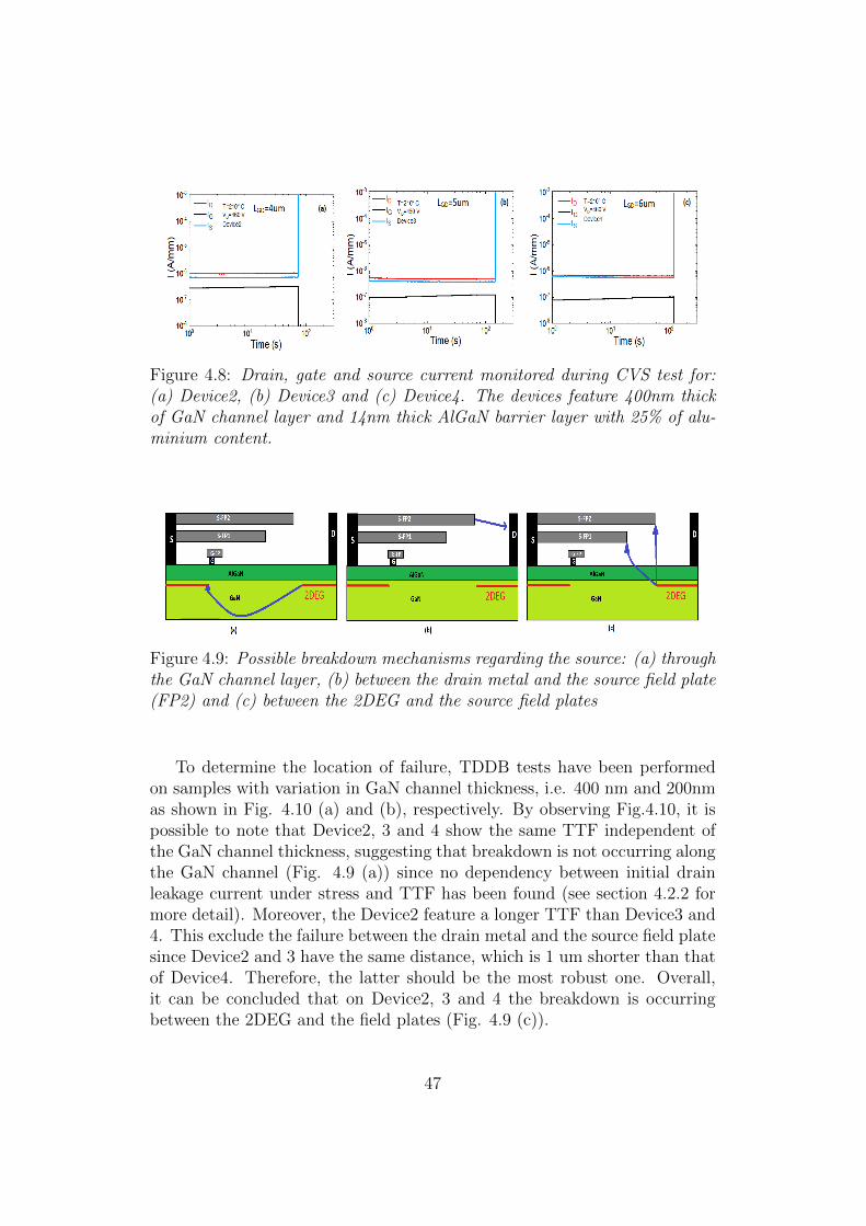
Figure 4.8: Drain, gate and source current monitored during CVS test for:(a) Device2, (b) Device3 and (c) Device4. The devices feature 400nm thickof GaN channel layer and 14nm thick AlGaN barrier layer with 25% of alu-minium content.
Figure 4.9: Possible breakdown mechanisms regarding the source: (a) throughthe GaN channel layer, (b) between the drain metal and the source field plate(FP2) and (c) between the 2DEG and the source field plates
To determine the location of failure, TDDB tests have been performedon samples with variation in GaN channel thickness, i.e. 400 nm and 200nmas shown in Fig. 4.10 (a) and (b), respectively. By observing Fig.4.10, it ispossible to note that Device2, 3 and 4 show the same TTF independent ofthe GaN channel thickness, suggesting that breakdown is not occurring alongthe GaN channel (Fig. 4.9 (a)) since no dependency between initial drainleakage current under stress and TTF has been found (see section 4.2.2 formore detail). Moreover, the Device2 feature a longer TTF than Device3 and4. This exclude the failure between the drain metal and the source field platesince Device2 and 3 have the same distance, which is 1 um shorter than thatof Device4. Therefore, the latter should be the most robust one. Overall,it can be concluded that on Device2, 3 and 4 the breakdown is occurringbetween the 2DEG and the field plates (Fig. 4.9 (c)).
47

Figure 4.10: Time to failure distribution for the Device2 (red), Device3 (blu)and Device4 (yellow) with (a) TGaN=400nm and (b) TGaN=200nm. For bothcases TAlGaN is 14m with th 25% of aluminum. The TTF values are carriedout from constant voltage stress tests at 210o C with VD=460V.
To understand the reason why Device2 features a longer TTF comparedto Device3 and 4, TCAD simulations have been performed to monitor theelectric field distribution in the region below the field plates, i.e. the regioninterested by the failure during off-state stress. Fig. 4.11 shows the electricfield distribution at VD= 460 V for the 3 devices with different LGD andfield plates lengths summarized in table 4.1. In particular, although thedifferences in LGD and field plate lengths, the electric field is more or lesssimilar in all devices (see Fig. 4.12) whereas the area exposed to high electricfield is smaller in Device2 (are below FP2 and FP3) because of the shorterfield plates. As a result, similar electric field across a larger area produces ashorter time-to-failure, since TTF (or TTB) is strongly area-dependent.
Figure 4.11: TCAD electric field simulations for the Device2, Device3 andDevice4.
48

In conclusion, with longer gate-to-drain distance it is possible to obtainhigher breakdown voltages (Fig. 4.6), however, it is not a good solutionto improve the off-state reliability since, as shown in Fig. 4.10, there is nosignificant TFF difference between Device 3 and 4 (same field plate config-uration and different LGD). On the contrary, by optimizing the field platesgeometry, the lifetime can be significantly improved, allowing to reduce LGD,thus reducing the drain-to-source resistance during on-state operation.So, it is worth noticing that for shorter LGD the breakdown voltage is reduced(around 550V) but, it is enough to be above the operating voltage (200V).
Figure 4.12: Electric field distribution closer the FP1 and FP2 extrapolatedby TCAD simulations for the Device2, Device3 and Device4 with VD=460V.
4.2.1 Role of the AlGaN on off-state reliability.
Established the location of the failure on device with LGD≥4µm, i.e. betweenthe 2DEG and the source field plates (FP2 and/or FP3), the material layers inbetween (e.g. the AlGaN barrier) could play a fundamental role on the TTF.Consequently, a off-state reliability analysis has been performed on devicesfeaturing different AlGaN properties. It is worth noting that, because of itshigher robustness, only Device2 have been adopted for such investigation.Fig. 4.13 shows the Weibull plots, carried out from CVS tests, for threedifferent TAlGaN values: 12.5nm (Fig. 4.13(a)), 14nm (Fig. 4.13(b)) and16nm (Fig. 4.13(c)). The GaN channel layer thickness is 400nm and the Alcontent in AlGaN layer is 25%. For all the three thickness the TTF valuesare Weibull distributed with a slope (β) around 1.3, meaning that TTF is
49

induced by the same degradation mechanism.
Figure 4.13: Weibull plots of the constant voltage stress for the Device2, atdifferent AlGaN barrier layer thickness: (a) 12.5nm, (b) 14nm and (c) 16nm.
From the data presented in Fig. 4.13, the lifetime has been extrapolatedfor the devices with different AlGaN thickness, as shown in Fig. 4.14 (a) and4.14 (b). The failure criterion is 1% at 210o C. In particular, by observingFig. 4.14 (a) it is possible to note that the thicker the AlGaN, the longer theTTF, confirming on more time the failure location, i.e. between 2DEG andsource field plates.
Figure 4.14: Lifetime plot of the constant voltage stress for different AlGaNbarrier layer thickness (a). Drain voltage for ten years of lifetime versus theAlGaN barrier thickness.
In particular, with a thicker AlGaN barrier two possible situations canoccur: i) if the voltage drop across the barrier does not change, the electric
50
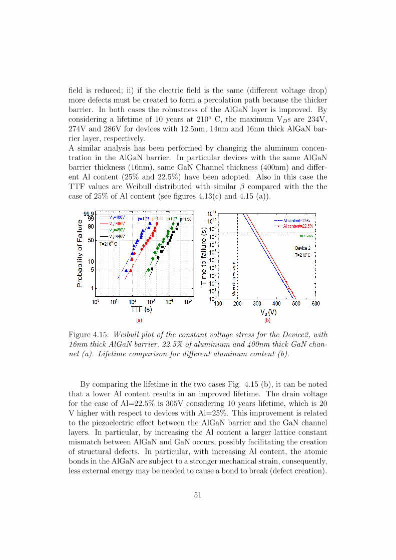
field is reduced; ii) if the electric field is the same (different voltage drop)more defects must be created to form a percolation path because the thickerbarrier. In both cases the robustness of the AlGaN layer is improved. Byconsidering a lifetime of 10 years at 210o C, the maximum VDs are 234V,274V and 286V for devices with 12.5nm, 14nm and 16nm thick AlGaN bar-rier layer, respectively.A similar analysis has been performed by changing the aluminum concen-tration in the AlGaN barrier. In particular devices with the same AlGaNbarrier thickness (16nm), same GaN Channel thickness (400nm) and differ-ent Al content (25% and 22.5%) have been adopted. Also in this case theTTF values are Weibull distributed with similar β compared with the thecase of 25% of Al content (see figures 4.13(c) and 4.15 (a)).
Figure 4.15: Weibull plot of the constant voltage stress for the Device2, with16nm thick AlGaN barrier, 22.5% of aluminium and 400nm thick GaN chan-nel (a). Lifetime comparison for different aluminum content (b).
By comparing the lifetime in the two cases Fig. 4.15 (b), it can be notedthat a lower Al content results in an improved lifetime. The drain voltagefor the case of Al=22.5% is 305V considering 10 years lifetime, which is 20V higher with respect to devices with Al=25%. This improvement is relatedto the piezoelectric effect between the AlGaN barrier and the GaN channellayers. In particular, by increasing the Al content a larger lattice constantmismatch between AlGaN and GaN occurs, possibly facilitating the creationof structural defects. In particular, with increasing Al content, the atomicbonds in the AlGaN are subject to a stronger mechanical strain, consequently,less external energy may be needed to cause a bond to break (defect creation).
51

It is worth noting that, in order to have failure between 2DEG and sourcefield plate the percolation path must be created in both AlGaN barrier layerand passivation layer. Further analyses are needed to understand who isfailing earlier.
4.2.2 From surface to bulk failure
Fig. 4.16 shows the monitored drain current during CVS test for the Device1with different TGaN and TAlGaN . In particular, in Fig. 4.16 (a) it is shownthat decreasing the GaN channel layer thickness, the drain leakage currentis lower and the TTF is higher. The same behaviour can be observed byincreasing the AlGaN layer thickness Fig. 4.16 (b).
Figure 4.16: Drain current of the Device1 (LGD=3µm) during CVS tests fordifferent TGaN with the same TAlGaN (14nm) and Al content (25%) (a) andfor different TAlGaN with the same TGaN (400nm) and Al content (25%) (b).
Since, Device1 has the shortest gate-to-drain distance (LGD = 3µm), themotivation of such behaviour can be related to short channel effects, such aspunch-through or drain induced barrier lowering (DIBL). Therefore, unlikedevices with LGD ≥ 4um, Device1 can be affected by breakdown occurringin the GaN channel. In this case, the depletion of the GaN channel layercan play a fundamental role. If the GaN channel layer under the gate ispartially depleted, the drain leakage subjected to high longitudinal electricfield is higher, promoting the creation of defects hence of the breakdown. InFig. 4.17 the TTF versus the inverse of the initial drain leakage during thestress is shown. A strong dependency is observed for different GaN (4.17 (a))
52

and AlGaN thicknesses (4.17 (b)).In particular, by increasing the AlGaN thickness the 2DEG density increasesas well because of the higher spontaneous polarization. As a result, the higherthe 2DEG density, the greater the difficulty to deplete such charge. Conse-quently, the extension of the related depletion region is limited, promotinghigher drain leakage, thus shorter TTF. This phenomenon is attenuated bydecreasing TGaN since the undepleted GaN layer is reduced.
Figure 4.17: Correlation between the drain leakage current (ID), monitored atthe beginning of the stress, for different TGaN with the same TAlGaN (14nm)and Al content (25%) (a) and for different TAlGaN with the same TGaN
(400nm) and Al content (25%) (b), for the Device1.
Figure 4.18: Correlation between the drain leakage current (ID), monitoredat the beginning of the stress, and the time-to-failure for the Device2 (a),Device3 (b) and Device4 (c).
To further demonstrate the occurrence of the breakdown in the GaNchannel layer in the case of devices with LGD=3µm, a similar investigation
53

has been provided for Device2, 3 and 4. In particular, in Fig. 4.18, the lackof TTF dependency on the initial drain leakage during the stress is shown.In particular, unlike the Device1, by changing the GaN channel thickness nodependency is shown. This confirm that: i) if the LGD is shorter than 4µmthe breakdown occurs in the GaN channel (400nm); ii) if longer than 4µmthe failure occurs at the surface between 2DEG and source field plates.Fig. 4.19 shows the time-to-failure distribution by varying TGaN (4.19 (a))and TAlGaN (4.19 (b)). Note that two different TTF scales are adopted forthe two figures. However, as already discussed, the thinner the AlGaN barrierand the GaN channel layers, the longer the TTF. Finally, the lifetime hasbeen evaluated for the two device groups marked by the red boxes, i.e. (1)TGaN=200nm and TAlGaN=14nm, (2) TGaN=400nm and TAlGaN=12.5nm.
Figure 4.19: Time to failure distribution for the Device1 for different TGaN
with the same TAlGaN (14nm) and Al content (25%) (a) and for differ-ent TAlGaN with the same TGaN (400nm) and Al content (25%) (b). TheTTF values are carried out from constant voltage stress tests at 210o C withVD=430V, for the Device1.
In the first case by performing CVS test at four different voltages, theTTF values are Weibull distributed with β∼1.4, as shown in Fig. 4.20 (a).Although, the TTF are Weibull distributed, the lifetime at 1% of failure doesnot respect the target of 200V for ten years (4.20 (b)).A strong improvement is noticed for the second case (Fig. 4.21). In particu-lar, the extrapolated maximum drain voltage which guarantees a lifetime of10 years at 210o C, considering 1% as failure criterion, is 262 V. The latteris higher than devices operating voltage (200 V). This means that by de-creasing the GaN channel layer thickness the short channel effect, causing a
54

premature failure, can be suppressed.
Figure 4.20: Weibull plot of the constant voltage stress for the Device1, with12.5nm thick AlGaN barrier, 25% of aluminium and 400nm thick GaN chan-nel (a). (b) Extrapolated lifetime from (a).
Figure 4.21: Weibull plot of the constant voltage stress for the Device1, with14nm thick AlGaN barrier, 25% of aluminium and 200nm thick GaN channel(a). (b) Extrapolated lifetime from (a).
In table 4.2, the extrapolated lifetime, shown in this chapter, are summa-rized.
55
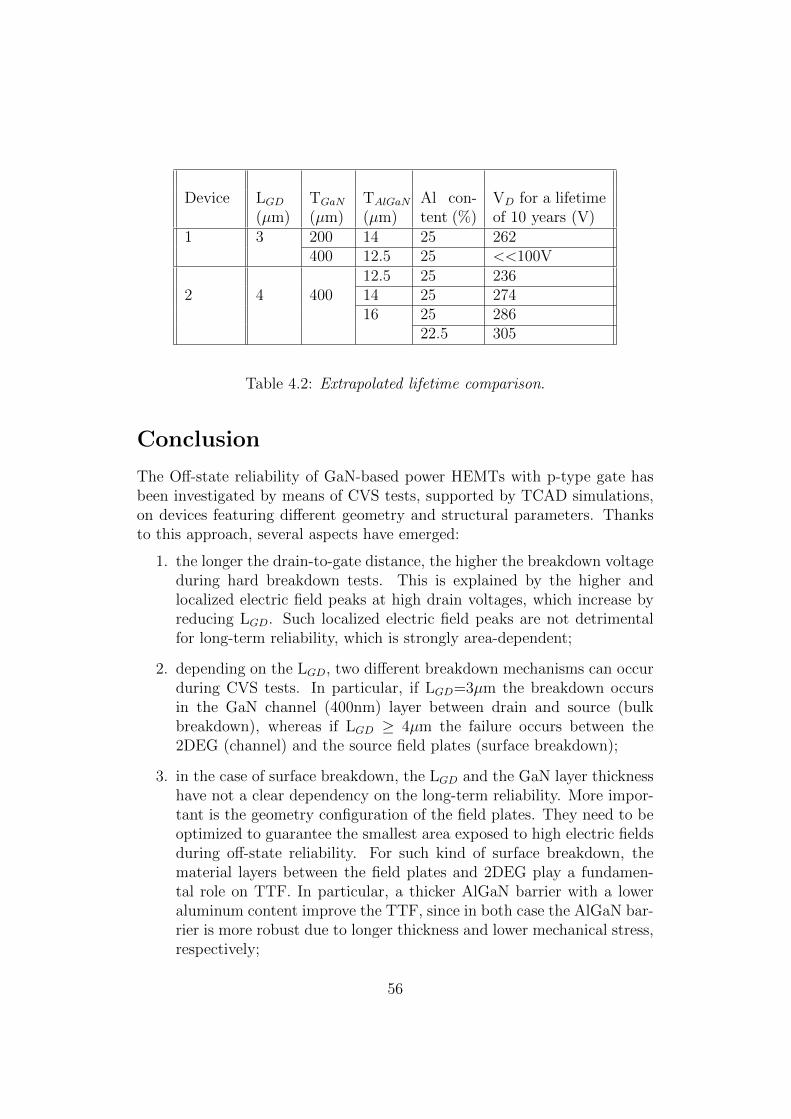
Device LGD(µm)
TGaN
(µm)TAlGaN
(µm)Al con-tent (%)
VD for a lifetimeof 10 years (V)
1 3 200 14 25 262400 12.5 25 <<100V
12.5 25 2362 4 400 14 25 274
16 25 28622.5 305
Table 4.2: Extrapolated lifetime comparison.
Conclusion
The Off-state reliability of GaN-based power HEMTs with p-type gate hasbeen investigated by means of CVS tests, supported by TCAD simulations,on devices featuring different geometry and structural parameters. Thanksto this approach, several aspects have emerged:
1. the longer the drain-to-gate distance, the higher the breakdown voltageduring hard breakdown tests. This is explained by the higher andlocalized electric field peaks at high drain voltages, which increase byreducing LGD. Such localized electric field peaks are not detrimentalfor long-term reliability, which is strongly area-dependent;
2. depending on the LGD, two different breakdown mechanisms can occurduring CVS tests. In particular, if LGD=3µm the breakdown occursin the GaN channel (400nm) layer between drain and source (bulkbreakdown), whereas if LGD ≥ 4µm the failure occurs between the2DEG (channel) and the source field plates (surface breakdown);
3. in the case of surface breakdown, the LGD and the GaN layer thicknesshave not a clear dependency on the long-term reliability. More impor-tant is the geometry configuration of the field plates. They need to beoptimized to guarantee the smallest area exposed to high electric fieldsduring off-state reliability. For such kind of surface breakdown, thematerial layers between the field plates and 2DEG play a fundamen-tal role on TTF. In particular, a thicker AlGaN barrier with a loweraluminum content improve the TTF, since in both case the AlGaN bar-rier is more robust due to longer thickness and lower mechanical stress,respectively;
56
4. Finally, in the case of bulk breakdown, the GaN layer thickness play afundamental role, i.e. the thinner the longer TTF. It can be related toeffectiveness of the depletion region under the gate. If the GaN layeris partially depleted, the drain leakage subjected to high longitudinalelectric field (due to short LGD) is higher, promoting defects creationand shorter TTF. Similarly, by increasing the AlGaN thickness the2DEG density is higher, limiting the extension of the depletion region.This phenomenon can be suppressed by reducing the GaN thickness.
The tested p-GaN gate HEMTs designed for 200V operation feature an ex-trapolated 10 years lifetime at a voltage of 234V to 305V extending the targetoperating voltage of 200 V (see table 4.2).
57

Bibliography
[1] http://www.worldenergydata.org/world/.
[2] Jose Millan, Philippe Godignon, Xavier Perpina, Amador Perez-Tomas,and Jose Rebollo. A survey of wide bandgap power semiconductor de-vices. IEEE Transactions on Power Electronics, 29:2155–2163, 05 2014.
[3] Angelo Raciti, Santi Rizzo, Nunzio Salerno, Giovanni Susinni, Con-cettina Buccella, Carlo Cecati, and Mario Tinari. State of the art andemerging solid-state power devices in the perspective of more electricaircraft. 10 2018.
[4] N. Kaminski. State of the art and the future of wide band-gap devices.2009 13th European Conference on Power Electronics and Applications,EPE ’09, pages 1 – 9, 10 2009.
[5] B. J. Baliga. Power semiconductor device figure of merit for high-frequency applications. IEEE Electron Device Letters, 10(10):455–457,Oct 1989.
[6] E. Johnson. Physical limitations on frequency and power parameters oftransistors. In 1958 IRE International Convention Record, volume 13,pages 27–34, March 1965.
[7] B. J. Baliga. Semiconductors for high-voltage, vertical channel field-effect transistors. Journal of Applied Physics, 53(3):1759–1764, 1982.
[8] B. Baliga. Fundamentals of Power Semiconductor Devices. 01 2008.
[9] O. Hilt N. Kaminskim. Sic and gan devices – wide bandgap is not allthe same. Circuits, Devices & Systems, IET, 8:227–236, 05 2014.
[10] Oliver Ambacher, B. Foutz, Joseph Smart, J.R. Shealy, Nils Weimann,K. Chu, M. Murphy, AJ Sierakowski, William Schaff, L. Eastman,R. Dimitrov, A. Mitchell, and Martin Stutzmann. Two dimensional
59
electron gases induced by spontaneous and piezoelectric polarizationundoped and doped algan/gan heterostructures. Journal of AppliedPhysics, 87:334–344, 01 2000.
[11] O. Ambacher, J. Smart, J. R. Shealy, N. G. Weimann, K. Chu, M. Mur-phy, W. J. Schaff, L. F. Eastman, R. Dimitrov, L. Wittmer, M. Stutz-mann, W. Rieger, and J. Hilsenbeck. Two-dimensional electron gasesinduced by spontaneous and piezoelectric polarization charges in n-and ga-face algan/gan heterostructures. Journal of Applied Physics,85(6):3222–3233, 1999.
[12] Tsung Yu Chen, Cheng-Ta Kuo, Chi-Ling Lee, and Wei-I Lee. Studyof free-standing gan substrates prepared by hydride vapor phase epi-taxy technology. In Proceedings of the Sixth Chinese OptoelectronicsSymposium (IEEE Cat. No.03EX701), pages 46–49, Sep. 2003.
[13] M. Sumiya and S. Fuke. Review of polarity determination and controlof gan. MRS Internet Journal of Nitride Semiconductor Research, 9:e1,2004.
[14] L. Liu and J.H. Edgar. Substrates for gallium nitride epitaxy. MaterialsScience & Engineering R-reports - MAT SCI ENG R, 37:61–127, 042002.
[15] C. Mion, J. F. Muth, E. A. Preble, and D. Hanser. Accurate dependenceof gallium nitride thermal conductivity on dislocation density. AppliedPhysics Letters, 89(9):092123, 2006.
[16] F. Ruiz-Zepeda, O. Contreras, A. Dadgar, and A. Krost. Microstructureof gallium nitride films grown on silicon (110). Applied Physics Letters,96(23):231908, 2010.
[17] J. W. Chung, J. Lee, E. L. Piner, and T. Palacios. Seamless on-waferintegration of si(100) mosfets and gan hemts. IEEE Electron DeviceLetters, 30(10):1015–1017, Oct 2009.
[18] https://ecse.rpi.edu/~schubert/Light-Emitting-Diodes-dot-org/
chap12/chap12.htm.
[19] Gerald Stringfellow. Organometallic Vapor-Phase Epitaxy. 03 1999.
[20] Shuji Nakamura, Naruhito Iwasa, Masayuki Senoh, and Takashi Mukai.Hole compensation mechanism of p-type GaN films. Japanese Journalof Applied Physics, 31(Part 1, No. 5A):1258–1266, may 1992.
60
[21] L. B. Rowland, K. Doverspike, and D. K. Gaskill. Silicon doping of ganusing disilane. Applied Physics Letters, 66(12):1495–1497, 1995.
[22] H. Marchand, Liang Zhao, N. Zhang, Brendan Moran, R. Coffie, U.K.Mishra, James Speck, Steven Denbaars, and JA Freitas. Metalorganicchemical vapor deposition of gan on si(111): Stress control and applica-tion to field-effect transistors. Journal of Applied Physics, 89:7846–7851,06 2001.
[23] Domenica Visalli, Marleen Van Hove, Puneet Srivastava, Joff Derluyn,Johan Das, Maarten Leys, Stefan Degroote, Kai Cheng, Marianne Ger-main, and Gustaaf Borghs. Experimental and simulation study of break-down voltage enhancement of algan/gan heterostructures by si substrateremoval. Applied Physics Letters, 97(11):113501, 2010.
[24] Deok Kyu Kim. Effect of aln buffer thickness on stress relaxation in ganlayer on si (111). Solid-State Electronics, 51(7):1005 – 1008, 2007.
[25] Kai Cheng, M. Leys, S. Degroote, B. Daele, S. Boeykens, Joff Derluyn,Marianne Germain, Gustaaf van Tendeloo, Jan Engelen, and GustaafBorghs. Flat gan epitaxial layers grown on si(111) by metalorganic vaporphase epitaxy using step-graded algan intermediate layers. Journal ofElectronic Materials, 35:592–598, 04 2006.
[26] Eric Feltin, Brad Beaumont, M. Laugt, P. Mierry, Philippe Vennegues,H. Lahreche, M. Leroux, and P. Gibart. Stress control in gan grownon silicon (111) by metalorganic vapor phase epitaxy. Applied PhysicsLetters, 79:3230–3232, 11 2001.
[27] M. J. Uren, M. Silvestri, M. Casar, G. A. M. Hurkx, J. A. Croon,J. Sonsky, and M. Kuball. Intentionally carbon-doped algan/gan hemts:Necessity for vertical leakage paths. IEEE Electron Device Letters,35(3):327–329, March 2014.
[28] O. Hilt, F. Brunner, E. Cho, A. Knauer, E. Bahat-Treidel, and J. Wurfl.Normally-off high-voltage p-gan gate gan hfet with carbon-doped buffer.In 2011 IEEE 23rd International Symposium on Power SemiconductorDevices and ICs, pages 239–242, May 2011.
[29] J. P. Ibbetson, P. T. Fini, K. D. Ness, S. P. DenBaars, J. S. Speck,and U. K. Mishra. Polarization effects, surface states, and the source ofelectrons in algan/gan heterostructure field effect transistors. AppliedPhysics Letters, 77(2):250–252, 2000.
61

[30] Ho Jang, Chang Jeon, Ki-Hong Kim, Jong Kyu Kim, Bae Sung Bum,Jung-Hee Lee, Jae Choi, and Jong-Lam Lee. Mechanism of two-dimensional electron gas formation in alxga1-xn/gan heterostructures.Applied Physics Letters, 81:1249 – 1251, 09 2002.
[31] E. Yu, X. Dang, L. Yu, Dayong Qiao, P. Asbeck, S. Lau, G. Sullivan,Karim Boutros, and Joan Redwing. Schottky barrier engineering in iii–vnitrides via the piezoelectric effect. Applied Physics Letters, 73:1880–1882, 09 1998.
[32] Giorgia Longobardi, Florin Udrea, Stephen Sque, Jeroen Croon, FredHurkx, E. Napoli, and J. Sonsky. Modelling 2deg charges in algan/ganheterostructures. volume 2, pages 363–366, 10 2012.
[33] Sten Heikman, Stacia Keller, Yuan Wu, James S. Speck, Steven P.DenBaars, and Umesh K. Mishra. Polarization effects in algan/-gan and gan/algan/gan heterostructures. Journal of Applied Physics,93(12):10114–10118, 2003.
[34] T. R. Prunty, J. A. Smart, E. N. Chumbes, B. K. Ridley, L. F. Eastman,and J. R. Shealy. Passivation of algan/gan heterostructures with siliconnitride for insulated gate transistors. In Proceedings 2000 IEEE/ CornellConference on High Performance Devices (Cat. No.00CH37122), pages208–214, Aug 2000.
[35] K. J. Chen, O. Haberlen, A. Lidow, C. l. Tsai, T. Ueda, Y. Uemoto, andY. Wu. Gan-on-si power technology: Devices and applications. IEEETransactions on Electron Devices, 64(3):779–795, March 2017.
[36] Fabrizio Roccaforte, Giuseppe Greco, Patrick Fiorenza, and Iucolano.An overview of normally-off gan-based high electron mobility transistors.Materials, 12:1599, 05 2019.
[37] W. Saito, Y. Takada, M. Kuraguchi, K. Tsuda, and I. Omura. Recessed-gate structure approach toward normally off high-voltage algan/ganhemt for power electronics applications. IEEE Transactions on Elec-tron Devices, 53(2):356–362, Feb 2006.
[38] Y. Cai, Y. Zhou, K. M. Lau, and K. J. Chen. Control of thresholdvoltage of algan/gan hemts by fluoride-based plasma treatment: Fromdepletion mode to enhancement mode. IEEE Transactions on ElectronDevices, 53(9):2207–2215, Sep. 2006.
62

[39] Yuhao Zhang, Min Sun, Sameer Joglekar, Tatsuya Fujishima, and TomasPalacios. Threshold voltage control by gate oxide thickness in fluorinatedgan metal-oxide-semiconductor high-electron-mobility transistors. Ap-plied Physics Letters, 103, 07 2013.
[40] M. N. A. Aadit, S. G. Kirtania, and M. K. Alam. Dependence of thresh-old voltage on doped layer thickness in algan/gan hemt: An improvedsplit donor e-mode design. In 2016 5th International Conference on In-formatics, Electronics and Vision (ICIEV), pages 681–686, May 2016.
[41] N. E. Posthuma, S. You, H. Liang, N. Ronchi, X. Kang, D. Wellekens,Y. N. Saripalli, and S. Decoutere. Impact of mg out-diffusion and activa-tion on the p-gan gate hemt device performance. In 2016 28th Interna-tional Symposium on Power Semiconductor Devices and ICs (ISPSD),pages 95–98, June 2016.
[42] F. Lee, L. Su, C. Wang, Y. Wu, and J. Huang. Impact of gate metal onthe performance of p-gan/algan/gan high electron mobility transistors.IEEE Electron Device Letters, 36(3):232–234, March 2015.
[43] O.; Wurfl J.; Meneghesso G. Meneghini, M.; Hilt. Technology and reli-ability of normally-off gan hemts with p-type gate. Energies 2017.
[44] Infineon. https://www.infineon.com/cms/en/product/power/
wide-band-gap-semiconductors-sic-gan/gallium-nitride-gan/.
[45] GaN systems. https://gansystems.com/.
[46] Panasonic. https://eu.industrial.panasonic.com/products/
semiconductors/gan-power/.
[47] K. Kim, S. Jung, D. Kim, H. Kang, K. Im, J. Oh, J. Ha, J. Shin, andJ. Lee. Effects of tmah treatment on device performance of normally offAl2O3/GaN mosfet. IEEE Electron Device Letters, 32(10):1376–1378,Oct 2011.
[48] Y.; Kokawa T.; Ikeda N.; Nomura T.; Kato S. Kambayashi, H.; Satoh.High field-effect mobility normallyoff algan/gan hybrid mos-hfeton sisubstrate by selective area growth technique. Solid-State Electron.,56:163–167, 2011.
[49] Mengyuan Hua, Zhaofu Zhang, Jin Wei, Jiacheng Lei, Gaofei Tang, KaiFu, Yong Cai, Baoshun Zhang, and Kevin J. Chen. Integration of lpcvd-sinx gate dielectric with recessed-gate e-mode gan mis-fets: Toward high
63

performance, high stability and long tddb lifetime. 2016 IEEE Interna-tional Electron Devices Meeting (IEDM), pages 10.4.1–10.4.4, 2016.
[50] D. Marcon, Marleen Van Hove, Brice Jaeger, N. Posthuma, DirkWellekens, S. You, Xuanwu Kang, Tian-Li Wu, Maarten Willems, SteveStoffels, and S. Decoutere. Direct comparison of gan-based e-mode ar-chitectures (recessed mishemt and p-gan hemts) processed on 200mmgan-on-si with au-free technology. Proceedings of SPIE - The Interna-tional Society for Optical Engineering, 9363, 03 2015.
[51] Sylvain Delage and Christian Dua. Wide band gap semiconductor reli-ability : Status and trends. Microelectronics Reliability, 43:1705–1712,09 2003.
[52] S. C. Binari, P. B. Klein, and T. E. Kazior. Trapping effects in ganand sic microwave fets. Proceedings of the IEEE, 90(6):1048–1058, June2002.
[53] R. Vetury, N. Q. Zhang, S. Keller, and U. K. Mishra. The impact ofsurface states on the dc and rf characteristics of algan/gan hfets. IEEETransactions on Electron Devices, 48(3):560–566, March 2001.
[54] P. B. Klein, S. C. Binari, K. Ikossi, A. E. Wickenden, D. D. Koleske,and R. L. Henry. Current collapse and the role of carbon in algan/ganhigh electron mobility transistors grown by metalorganic vapor-phaseepitaxy. Applied Physics Letters, 79(21):3527–3529, 2001.
[55] S. J. Pearton, J. C. Zolper, R. J. Shul, and F. Ren. Gan: Processing,defects, and devices. Journal of Applied Physics, 86(1):1–78, 1999.
[56] P. J. Hansen, Y. E. Strausser, A. N. Erickson, E. J. Tarsa, P. Kozodoy,E. G. Brazel, J. P. Ibbetson, U. Mishra, V. Narayanamurti, S. P. Den-Baars, and J. S. Speck. Scanning capacitance microscopy imaging ofthreading dislocations in gan films grown on (0001) sapphire by metalor-ganic chemical vapor deposition. Applied Physics Letters, 72(18):2247–2249, 1998.
[57] A. F. Wright and U. Grossner. The effect of doping and growth stoi-chiometry on the core structure of a threading edge dislocation in gan.Applied Physics Letters, 73(19):2751–2753, 1998.
[58] J. Joh and J. A. del Alamo. A current-transient methodology for trapanalysis for gan high electron mobility transistors. IEEE Transactionson Electron Devices, 58(1):132–140, Jan 2011.
64
[59] A. Telia L. Semra and A. Soltani. Trap characterization in algan/ganhemt by analyzing frequency dispersion in capacitance and conductance.Surface and Interface Analysis, 42(6-7):799–802, 2010.
[60] Gaudenzio Meneghesso, Matteo Meneghini, Davide Bisi, Isabella Ros-setto, Andrea Cester, Umesh K Mishra, and Enrico Zanoni. Trap-ping phenomena in AlGaN/GaN HEMTs: a study based on pulsedand transient measurements. Semiconductor Science and Technology,28(7):074021, jun 2013.
[61] P. Lagger, P. Steinschifter, M. Reiner, M. Stadtmuller, G. Denifl,A. Naumann, J. Muller, L. Wilde, J. Sundqvist, D. Pogany, and C. Os-termaier. Role of the dielectric for the charging dynamics of the dielec-tric/barrier interface in algan/gan based metal-insulator-semiconductorstructures under forward gate bias stress. Applied Physics Letters,105(3):033512, 2014.
[62] M. Ruzzarin, M. Meneghini, I. Rossetto, M. Van Hove, S. Stoffels,T. Wu, S. Decoutere, G. Meneghesso, and E. Zanoni. Evidence of hot-electron degradation in gan-based mis-hemts submitted to high tem-perature constant source current stress. IEEE Electron Device Letters,37(11):1415–1417, Nov 2016.
[63] T. Wu, D. Marcon, S. You, N. Posthuma, B. Bakeroot, S. Stof-fels, M. Van Hove, G. Groeseneken, and S. Decoutere. Forward biasgate breakdown mechanism in enhancement-mode p-gan gate algan/-gan high-electron mobility transistors. IEEE Electron Device Letters,36(10):1001–1003, Oct 2015.
[64] A. N. Tallarico, S. Stoffels, P. Magnone, N. Posthuma, E. Sangiorgi,S. Decoutere, and C. Fiegna. Investigation of the p-gan gate breakdownin forward-biased gan-based power hemts. IEEE Electron Device Letters,38(1):99–102, Jan 2017.
[65] A. N. Tallarico, S. Stoffels, N. Posthuma, S. Decoutere, E. Sangiorgi, andC. Fiegna. Threshold voltage instability in gan hemts with p-type gate:Mg doping compensation. IEEE Electron Device Letters, 40(4):518–521,April 2019.
[66] L. Efthymiou, G. Longobardi, G. Camuso, T. Chien, M. Chen, andF. Udrea. On the physical operation and optimization of the p-gan gate in normally-off gan hemt devices. Applied Physics Letters,110(12):123502, 2017.
65

[67] M. Meneghini, I. Rossetto, C. De Santi, F. Rampazzo, A. Tajalli, A. Bar-bato, M. Ruzzarin, M. Borga, E. Canato, E. Zanoni, and G. Meneghesso.Reliability and failure analysis in power gan-hemts: An overview. In2017 IEEE International Reliability Physics Symposium (IRPS), pages3B–2.1–3B–2.8, April 2017.
[68] C. Zhou, Q. Jiang, S. Huang, and K. J. Chen. Vertical leakage/break-down mechanisms in algan/gan-on-si structures. In 2012 24th Inter-national Symposium on Power Semiconductor Devices and ICs, pages245–248, June 2012.
[69] I. B. Rowena, S. L. Selvaraj, and T. Egawa. Buffer thickness contribu-tion to suppress vertical leakage current with high breakdown field (2.3mv/cm) for gan on si. IEEE Electron Device Letters, 32(11):1534–1536,Nov 2011.
[70] M. Marso, M. Wolter, P. Javorka, P. Kordos, and H. Luth. Investigationof buffer traps in an algan/gan/si high electron mobility transistor bybackgating current deep level transient spectroscopy. Applied PhysicsLetters, 82(4):633–635, 2003.
[71] M. Borga, M. Meneghini, S. Stoffels, X. Li, N. Posthuma, M. Van Hove,S. Decoutere, G. Meneghesso, and E. Zanoni. Impact of substrate resis-tivity on the vertical leakage, breakdown, and trapping in gan-on-si e-mode hemts. IEEE Transactions on Electron Devices, 65(7):2765–2770,July 2018.
[72] H. Umeda, A. Suzuki, Y. Anda, M. Ishida, T. Ueda, T. Tanaka, andD. Ueda. Blocking-voltage boosting technology for gan transistors bywidening depletion layer in si substrates. In 2010 International ElectronDevices Meeting, pages 20.5.1–20.5.4, Dec 2010.
[73] M. G. Ancona, S. C. Binari, and D. Meyer. Fully-coupled electrome-chanical analysis of stress-related failure in gan hemts. physica statussolidi c, 8(7-8):2276–2278, 2011.
[74] Prashanth Makaram, Jungwoo Joh, Jesus A. del Alamo, Tomas Palacios,and Carl V. Thompson. Evolution of structural defects associated withelectrical degradation in algan/gan high electron mobility transistors.Applied Physics Letters, 96(23):233509, 2010.
[75] Feng Gao, Bin Lu, Libing Li, Stephen Kaun, James S. Speck, Carl. V.Thompson, and Tomas Palacios. Role of oxygen in the off-state degra-
66

dation of algan/gan high electron mobility transistors. Applied PhysicsLetters, 99(22):223506, 2011.
[76] F. Gao, D. Chen, B. Lu, H. L. Tuller, C. V. Thompson, S. Keller,U. K. Mishra, and T. Palacios. Impact of moisture and fluorocarbonpassivation on the current collapse of algan/gan hemts. IEEE ElectronDevice Letters, 33(10):1378–1380, Oct 2012.
[77] D. Marcon, T. Kauerauf, F. Medjdoub, J. Das, M. Van Hove, P. Sri-vastava, K. Cheng, M. Leys, R. Mertens, S. Decoutere, G. Meneghesso,E. Zanoni, and G. Borghs. A comprehensive reliability investigation ofthe voltage-, temperature- and device geometry-dependence of the gatedegradation on state-of-the-art gan-on-si hemts. In 2010 InternationalElectron Devices Meeting, pages 20.3.1–20.3.4, Dec 2010.
[78] P. Marko, M. Meneghini, S. Bychikhin, D. Marcon, G. Meneghesso,E. Zanoni, and D. Pogany. Iv, noise and electroluminescence analysisof stress-induced percolation paths in algan/gan high electron mobilitytransistors. Microelectronics Reliability, 52(9):2194 – 2199, 2012. SPE-CIAL ISSUE 23rd EUROPEAN SYMPOSIUM ON THE RELIABIL-ITY OF ELECTRON DEVICES, FAILURE PHYSICS AND ANALY-SIS.
[79] H.B. Dietrich G. Kelner A.E. Wickenden C. Binari, W. Kruppa andJ.A. FreitasJr. Fabrication and characterization of gan fets. Solid-StateElectronics, 41(10):1549–1554, 1997.
[80] I. Rossetto, M. Meneghini, S. Pandey, M. Gajda, G. A. M. Hurkx, J. A.Croon, J. Sonsky, G. Meneghesso, and E. Zanoni. Field-related failureof gan-on-si hemts: Dependence on device geometry and passivation.IEEE Transactions on Electron Devices, 64(1):73–77, Jan 2017.
[81] M. J. Uren, K. J. Nash, R. S. Balmer, T. Martin, E. Morvan, N. Cail-las, S. L. Delage, D. Ducatteau, B. Grimbert, and J. C. De Jaeger.Punch-through in short-channel algan/gan hfets. IEEE Transactionson Electron Devices, 53(2):395–398, Feb 2006.
[82] M. Meneghini, G. Cibin, M. Bertin, G. A. M. Hurkx, P. Ivo, J. Sonsky,J. A. Croon, G. Meneghesso, and E. Zanoni. Off-state degrada-tion of algan/gan power hemts: Experimental demonstration of time-dependent drain-source breakdown. IEEE Transactions on Electron De-vices, 61(6):1987–1992, June 2014.
67

[83] Eldad Bahat-Treidel, Oliver Hilt, Fank Brunner, Joachim Wurfl, andGunther Trankle. Punch-through voltage enhancement scaling of al-gan/gan hemts using algan double heterojunction confinement. physicastatus solidi c, 6(6):1373–1377, 2009.
[84] N. E. Posthuma, S. You, S. Stoffels, H. Liang, M. Zhao, and S. De-coutere. Gate architecture design for enhancement mode p-gan gatehemts for 200 and 650v applications. In 2018 IEEE 30th InternationalSymposium on Power Semiconductor Devices and ICs (ISPSD), pages188–191, May 2018.
[85] R. Degraeve, B. Kaczer, and G. Groeseneken. Degradation and break-down in thin oxide layers: mechanisms, models and reliability prediction.Microelectronics Reliability, 39(10):1445 – 1460, 1999.
[86] R. Degraeve, G. Groeseneken, R. Bellens, J. L. Ogier, M. Depas, P. J.Roussel, and H. E. Maes. New insights in the relation between electrontrap generation and the statistical properties of oxide breakdown. IEEETransactions on Electron Devices, 45(4):904–911, April 1998.
[87] P. Moens, A. Banerjee, P. Coppens, A. Constant, P. Vanmeerbeek, Z. Li,F. Declercq, L. De Schepper, H. De Vleeschouwer, C. Liu, B. Padman-abhan, W. Jeon, J. Guo, A. Salih, and M. Tack. Technology and designof gan power devices. In 2015 45th European Solid State Device ResearchConference (ESSDERC), pages 64–67, Sep. 2015.
[88] M. Borga, M. Meneghini, I. Rossetto, S. Stoffels, N. Posthuma, M. VanHove, D. Marcon, S. Decoutere, G. Meneghesso, and E. Zanoni. Evi-dence of time-dependent vertical breakdown in gan-on-si hemts. IEEETransactions on Electron Devices, 64(9):3616–3621, Sep. 2017.
[89] T. Kauerauf. Degradation and breakdown of mos gate stacks with highpermittivity dielectrics. PhD thesis, Faculty Eng., Katholieke Univ.,Leuven, Belgium, 2007.
68