Teoria dei Solidi, Fotonica, Nanostrutture -...
27
Teoria dei Solidi, Fotonica, Nanostrutture Dipartimento di Fisica, Università di Pavia & C.N.I.S.M. (Consorzio Nazionale Interuniversitario per le Scienze Fisiche della Materia) Giornata di orientamento L.M. in Scienze Fisiche - 23 Maggio 2013 Dario Gerace CNISM CNISM
Transcript of Teoria dei Solidi, Fotonica, Nanostrutture -...

Teoria dei Solidi, Fotonica, Nanostrutture
Dipartimento di Fisica, Università di Pavia &
C.N.I.S.M. (Consorzio Nazionale Interuniversitario per le Scienze Fisiche della Materia)
Giornata di orientamento L.M. in Scienze Fisiche - 23 Maggio 2013
Dario Gerace
CNISM CNISM
Teoria dei solidi, fotonica e nanostrutture – Dip. Fisica, Università di Pavia – http://fisica.unipv.it/nanophotonics
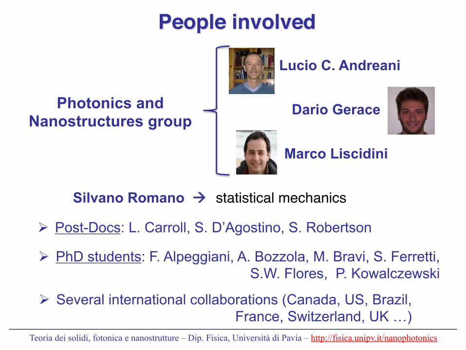
People involved!
Lucio C. Andreani
Marco Liscidini
Dario Gerace
Silvano Romano à statistical mechanics!
Photonics and Nanostructures group
Ø PhD students: F. Alpeggiani, A. Bozzola, M. Bravi, S. Ferretti, S.W. Flores, P. Kowalczewski
Ø Post-Docs: L. Carroll, S. D’Agostino, S. Robertson
Ø Several international collaborations (Canada, US, Brazil, France, Switzerland, UK …)

Teoria dei solidi, fotonica e nanostrutture – Dip. Fisica, Università di Pavia – http://fisica.unipv.it/nanophotonics
Condensed Matter Physics!Interested scales and ranges:
Energy scales à µeV - KeV
met
re
realm of electromagnetic interactions
Teoria dei solidi, fotonica e nanostrutture – Dip. Fisica, Università di Pavia – http://fisica.unipv.it/nanophotonics
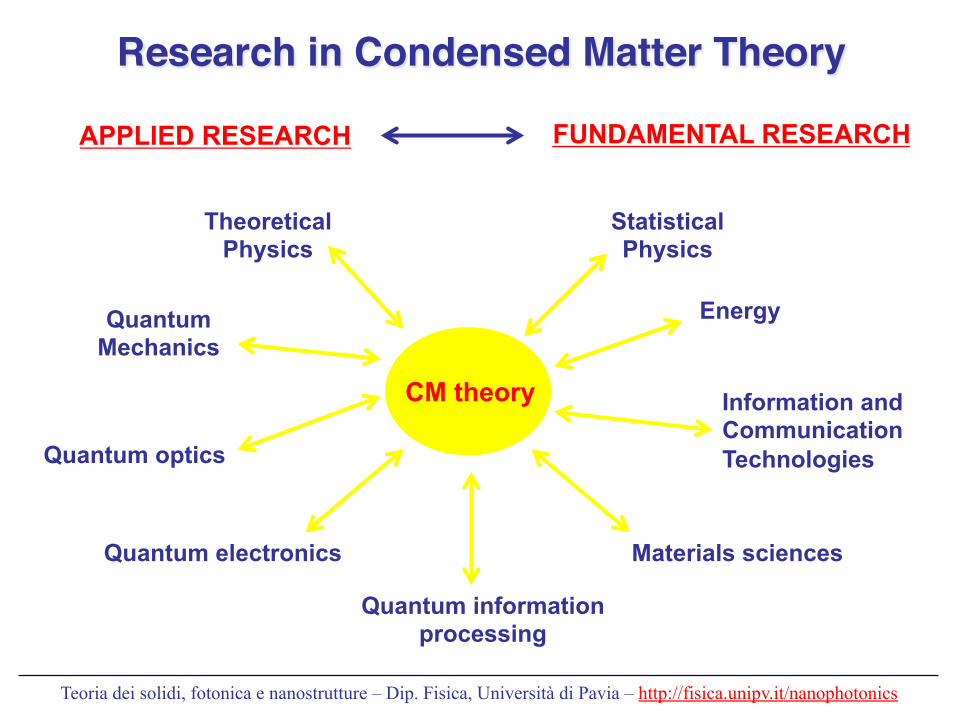
Research in Condensed Matter Theory!
CM theory
Theoretical Physics
Statistical Physics
Materials sciences
Quantum information processing
Quantum electronics
Quantum optics
Quantum Mechanics
Energy
Information and Communication Technologies
APPLIED RESEARCH FUNDAMENTAL RESEARCH

Teoria dei solidi, fotonica e nanostrutture – Dip. Fisica, Università di Pavia – http://fisica.unipv.it/nanophotonics
Active research lines
Ø Radiation-matter interaction in nanostructures
Ø Photonic Crystals: physics and applications
Ø Nonlinear and quantum photonics
Ø Statistical Mechanics of spins on lattices
Ø Photovoltaics
Ø Strongly correlated systems & analog models
Ø Plasmonics and superconductors

Teoria dei solidi, fotonica e nanostrutture – Dip. Fisica, Università di Pavia – http://fisica.unipv.it/nanophotonics
Ø Photonic Crystals: physics and applications

Teoria dei solidi, fotonica e nanostrutture – Dip. Fisica, Università di Pavia – http://fisica.unipv.it/nanophotonics
Photonic crystals photons in periodic dielectric media
“Photonic bands” and energy gaps, as in solids!
electrons in crystalline solids
Schrödinger equation 2nd-order Maxwell eqs. for harmonic fields

Teoria dei solidi, fotonica e nanostrutture – Dip. Fisica, Università di Pavia – http://fisica.unipv.it/nanophotonics
Photonics for telecom applications (Andreani-Gerace)
FABULOUS -FDMA Access By Using Low-cost Optical network Units in Silicon photonics , FP7-ICT-2011-8
Teoria dei solidi, fotonica e nanostrutture – Dip. Fisica, Università di Pavia – http://fisica.unipv.it/nanophotonics
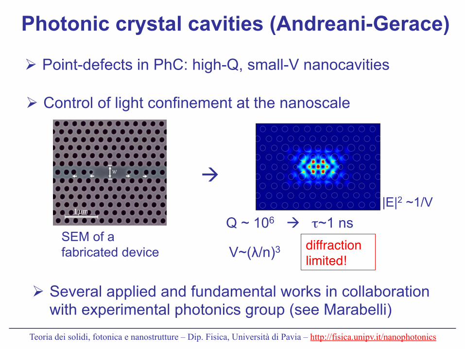
Photonic crystal cavities (Andreani-Gerace)
Ø Point-defects in PhC: high-Q, small-V nanocavities
Q ~ 106 à τ~1 ns |E|2 ~1/V
V~(λ/n)3 diffraction !limited!!
Ø Control of light confinement at the nanoscale
à
Ø Several applied and fundamental works in collaboration with experimental photonics group (see Marabelli)
SEM of a fabricated device

Teoria dei solidi, fotonica e nanostrutture – Dip. Fisica, Università di Pavia – http://fisica.unipv.it/nanophotonics
Ø Radiation-matter interaction in nanostructures

Teoria dei solidi, fotonica e nanostrutture – Dip. Fisica, Università di Pavia – http://fisica.unipv.it/nanophotonics
Semiconductor Nanostructures
-
+
Quantum confined electron-hole pairs in nanostructures
TEM image of a quantum dot
Bottom-up assembly of different semiconductors
Artificial atoms

Teoria dei solidi, fotonica e nanostrutture – Dip. Fisica, Università di Pavia – http://fisica.unipv.it/nanophotonics
Cavity Quantum Electro-Dynamics (Gerace)
BE
Ø Single (or a few) atom coupled to a high-Q/small-V resonator
model Traditionally used in atomic CQED
Ø Today applied to diverse nanostructured systems
MIUR - FIRB “giovani” project with NMR group
QD in PhC cavity
Spin ensemble in superconducting resonator
à 2012 Nobel Prize for Physics!

Teoria dei solidi, fotonica e nanostrutture – Dip. Fisica, Università di Pavia – http://fisica.unipv.it/nanophotonics
Bloch surface waves (Liscidini)
Ø Theoretical study of optical surface waves in periodic media.
Ø Connection with fundamental research in light-matter interaction (polaritons) and optical sensing (Raman, fluorescence).

Teoria dei solidi, fotonica e nanostrutture – Dip. Fisica, Università di Pavia – http://fisica.unipv.it/nanophotonics
Ø Photovoltaics

Teoria dei solidi, fotonica e nanostrutture – Dip. Fisica, Università di Pavia – http://fisica.unipv.it/nanophotonics
Photovoltaics: general Photovoltaic conversion in solar cells = optical problem (light trapping) + electronic problem (carrier collection) ⇒ ideal playground for photonics + semiconductors ⇒ with both fundamental aspects (efficiency limits) and applied ones ⇒ cultural opportunities, as well as funding and career ones

Teoria dei solidi, fotonica e nanostrutture – Dip. Fisica, Università di Pavia – http://fisica.unipv.it/nanophotonics
Photovoltaics research (Andreani-Liscidini)
Ø Fondazione Cariplo “Nanophotonics for thin-film photovoltaics” Ø ENI S.p.A. research contract “Photonics for photovoltaics systems based on fluorescent concentrators”
Focus of research: towards thin-film solar cells with high conversion efficiency – crucial for large-scale photovoltaic energy production in the long term.
Highlight: thin-film silicon solar cells can be more performing than bulk ones provided optimal (Lambertian) light trapping is applied (Bozzola et al., 2013, unpublished)
à Nanophotonics meets Photovoltaics
Light trapping à optimal thickness < 10 µm
No light trapping
Ø EU FP7 Marie Curie ITN Network PROPHET – “Postgraduate Research in Photonics as an Enabling Technology”

Teoria dei solidi, fotonica e nanostrutture – Dip. Fisica, Università di Pavia – http://fisica.unipv.it/nanophotonics
Ø Nonlinear and quantum photonics

Teoria dei solidi, fotonica e nanostrutture – Dip. Fisica, Università di Pavia – http://fisica.unipv.it/nanophotonics
Generation of entangled-photon pairs (Liscidini)
Ø Theoretical study and design of possible sources of quantum correlated photon pairs in nonlinear devices
Ø Connections to Quantum Mechanics, Quantum Computation and Quantum Information.
ωSignal ωPump ωIdler
2
Figure 1. (a) Emission of two photons by parametric fluores-cence; (b) Sketch of set-up for polarization resolved coinci-dence measurement; and (c) corresponding stimulated emis-sion configuration.
ditional experimental requirement, we demonstrate thatthe savings in time and improvement in precision are sogreat that this should become the preferred method forcharacterising sources of two-photon states generated byparametric fluorescence.
We consider the general situation sketched in Fig.1a, inwhich photon pairs are generated by SPDC in a genericstructure. The e↵ect of the nonlinearity in generatingthe downcoverted photons can be described by a for-mal transition at t = 0 from an asymptotic-in to anasymptotic-out state, with these states otherwise involv-ing only linear propagation, however complicated [9]. Ifthe probability of generating photons in each pair ofmodes (⌫k1, ⌘k2) is su�ciently small, then if a pair isgenerated the state describing the downconverted pho-tons can be written as [10]
|IIi = 1p2
X
⌫,⌘
Zdk1dk2�⌫⌘
(k1,k2)b†⌫k1
b†⌘k2
|vaci, (1)
(see supplemental material) where �⌫⌘
(k1,k2) is the nor-malized biphoton wave function, ⌫ and ⌘ indicate thepolarization of the generated photons, k1 and k2 are thewave vectors, and b†
⌫k1and b†
⌘k2are the corresponding
creation operators.A common experiment to characterise two-photon
sources is a set of coincidence measurements in a config-
uration similar to the one shown in Fig.1b, in which twosingle photon detectors count the photon-pairs generatedat wave vectors in the neighborhood of k3 and k3
0, andwith specified polarizations � and �0. Here we considerconfigurations in which the generated photons are eithernon-collinear or have di↵erent energies, such that theycan always be separated; thus we always have k3
0 6= k3.If one wants to reconstruct the biphoton wave function,the detection is done by taking small ranges �k3 and �k3
0
over which variation of the biphoton wave function can beconsidered negligible. In practice, in free space such a sit-uation can be realized using two pin-holes, which accountfor the filtering in the area transverse to the propagationdirection before the detectors, and optical filters, whichdefine the detection region in the direction parallel to k3
and k30. The average number of generated pairs in the
specified ranges is easily found to be
hb†�k3
b�k3b
†�
0k30b
�
0k30i�k3�k3
0
= 2|�|2���
�,�
0(k3,k30)��2 �k3�k3
0, (2)
where |�|2 is the probability that a pair of photons isgenerated.We now consider the case shown in Fig.1c, in which a
proper combination of incoming beams results in a co-herent state exiting from the structure with polarization�0 and centred at k3
0. The asymptotic-out state satisfies
B�
0k30 |B
�
0k30i = B
�
0k30 |B
�
0k30i (3)
where |B�
0k30 |2 is the average number of photons in the
coherent state, and
B†�
0k30 =
Zdkf
�
0k30(k)b†
�
0k (4)
with f�
0k30(k) a normalized function centred at k3
0. Forbulk crystals [6], optical fibers [11], and one-channel in-tegrated optical devices [12], the coherent state |B
�
0k03i
can be realized with a single input beam. For more com-plicated structures, the construction of |B
�
0k03i might re-
quire a combination of more than one input beam, but itcan always be obtained [9].
We consider the number of photons exiting from thestructure at k3 with polarization � (see Fig.1c); Thesephotons are generated by parametric fluorescence as wellas by the corresponding nonlinear process stimulated bythe coherent state, i.e., DFG [13]. The average numberof generated photons is
hb†�k3
b�k3i|B�0k3
0 i�k3 ⇡ 2|�|2X
⌘
Zdk|�
�⌘
(k3,k)|2�k3
+2|�|2|B�
0k30 |2
Zdk1dk2���
0(k3,k1)�⇤��
0(k3,k2)f⇤�
0k03(k1)f
�
0k03(k2)�k3, (5)
Stimulated and spontaneous four-wave mixing in silicon-on-insulator coupled photonicwire nano-cavities
Stefano Azzini,1 Davide Grassani,1 Matteo Galli,1 Dario Gerace,1 MaddalenaPatrini,1 Marco Liscidini,1 Philippe Velha,2 and Daniele Bajoni3, !
1Dipartimento di Fisica, Universita degli Studi di Pavia, via Bassi 6, 27100 Pavia, Italy2School of Engineering, University of Glasgow, Glasgow G12 8LT, UK
3Dipartimento di Ingegneria Industriale e dell’Informazione,Universita degli Studi di Pavia, via Ferrata 1, Pavia, Italy
(Dated: April 24, 2013)
We report on four-wave mixing in coupled photonic crystal nano-cavities on a silicon-on-insulatorplatform. Three photonic wire cavities are side-coupled to obtain three modes equally separatedin energy. The structure is designed to be self-filtering, and we show that the pump is rejected byalmost two orders of magnitudes. We study both the stimulated and the spontaneous four-wavemixing processes: owing to the small modal volume, we find that signal and idler photons aregenerated with a hundred-fold increase in e!ciency as compared to silicon micro-ring resonators.
PACS numbers: 42.65.Hw,42.70.Qs,42.82.Et
The adoption of photonic devices integrated on semi-conductor chips is increasing over the years. Circuitscontaining light sources, waveguides, and detectors havebeen successfully demonstrated and are used to routeinformation between components in high-end computersystems as well as in data centers. Silicon is by far themostly used material in a wide range of technological pro-cesses. Due to its strong refractive index contrast withair and silica, silicon-on-insulator (SOI) wafers can beprocessed in devices for e!cient confinement and propa-gation of light, such as photonic wire (PhW) waveguides.The goal of obtaining active functionalities in such de-vices has started a thorough investigation on silicon op-tical nonlinearities [1]. The inversion symmetry of thecrystalline unit cell prohibits second-order nonlinearitiesin bulk silicon, but third order nonlinear e"ects have beenreported, including Raman scattering [2, 3], Kerr nonlin-earity [4, 5] and two-photon absorption [6].
A common way to enhance optical nonlinearities is touse optical confinement to increase the overlap betweenthe electromagnetic field and the nonlinear material. Inthese regards, photonic crystals (PhCs) [7], and in par-ticular PhC nano-cavities [8], allow for the confinementof light to volumes comparable to the cube of their wave-length in the material and can be fabricated using sev-eral top-down approaches [9, 10] compatible with CMOStechnology [11, 12]. PhC cavities have been employedto enhance basic cavity quantum electrodynamics e"ects[13, 14], to demonstrate ultra-low threshold lasing [15, 16]and to enhance optical nonlinear e"ects in silicon [17–20].
In this work we use a PhC molecule (PCM) to achievefour-wave mixing (FWM) in a silicon integrated device.In order to achieve the energy conservation necessary forFWM, three resonances evenly separated in energy arenecessary [21]. One way to achieve this condition is toexploit the natural splitting in the resonances ot threecoupled identical cavities: this was first demonstrated for
one dimensional cavities in strong coupling with quantumwell excitons [22], but the same geometry can work withthree dimensional cavities in any material with a !(3)
optical nonlinearity.
FIG. 1: (color online) (a) SEM image of the SOI-integratedphotonic crystal molecule. (b) Left: SEM close-up view of thetriple cavity region, showing the cavity length c=620nm andthe coupling distance d=100nm. Right: FDTD-calculatedelectric field intensity cross-section of the three eigenmodesof the coupled structure along the dash-dotted yellow line (y-direction).
MIUR - FIRB “giovani” project (Bajoni - Liscidini)
Teoria dei solidi, fotonica e nanostrutture – Dip. Fisica, Università di Pavia – http://fisica.unipv.it/nanophotonics
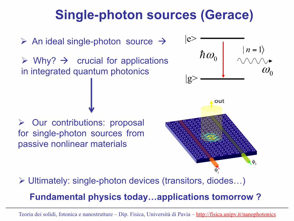
Single-photon sources (Gerace)
Ø Why? à crucial for applications in integrated quantum photonics
Ø Ultimately: single-photon devices (transitors, diodes…)
Ø Our contributions: proposal for single-photon sources from passive nonlinear materials
Ø An ideal single-photon source à |e>
|g>
〉=1| n0ω
0ω
Fundamental physics today…applications tomorrow ?

Teoria dei solidi, fotonica e nanostrutture – Dip. Fisica, Università di Pavia – http://fisica.unipv.it/nanophotonics
Ø Plasmonics and superconductors

Teoria dei solidi, fotonica e nanostrutture – Dip. Fisica, Università di Pavia – http://fisica.unipv.it/nanophotonics
Plasmonics PLASMONS are collective excitations of free electrons in a metal
They can LOCALIZE à surface plasmons
They can COUPLE TO RADIATION à surface plasmon polaritons
Electronic systems
Photonics PLASMONICS
+ - + - +
dielectric
metal
Vibrant field of research, with many fundamental aspects (control of radiative processes, sub-wavelength optics…) and applied ones (biosensors…)

Teoria dei solidi, fotonica e nanostrutture – Dip. Fisica, Università di Pavia – http://fisica.unipv.it/nanophotonics
Plasmonics research (Andreani) Ø Control of radiation-matter interaction, dipole-emission rates
Ø Surface-enhanced processes because of electric-field localization à Biosensors
Ø High-Tc superconductors: low-frequency plasma waves due to Josephson tunnelling along c-axis à Terahertz plasmons
à Connection with Terahertz photonics
à Possible link with mechanism of high-Tc superconductivity
Bi2Sr2CuO6+x

Teoria dei solidi, fotonica e nanostrutture – Dip. Fisica, Università di Pavia – http://fisica.unipv.it/nanophotonics
Ø Statistical Mechanics of spins on lattices

Teoria dei solidi, fotonica e nanostrutture – Dip. Fisica, Università di Pavia – http://fisica.unipv.it/nanophotonics
Statistical Mechanics (S. Romano)
Ø Statistical mechanics of Spin lattices
Ø Computational research on liquid phases of matter
Ø Study of thermodynamic and structural properties of systems of interacting many particles
RELATED COURSES (L.M. Chimica): Statistical Thermodynamics!Theoretical and Computational Chemistry!
Teoria dei solidi, fotonica e nanostrutture – Dip. Fisica, Università di Pavia – http://fisica.unipv.it/nanophotonics
Ø Strongly correlated systems & analog models

Teoria dei solidi, fotonica e nanostrutture – Dip. Fisica, Università di Pavia – http://fisica.unipv.it/nanophotonics
Strongly correlated systems (Gerace-Andreani)
Ø The physics of interacting quasi-particles (electrons, polaritons, phonons, plasmons, magnons, …)
Ø Manybody theory…techniques from QFT phonon
Analog models (Gerace) Ø Studying systems with formal analogies with known models in
theoretical physics
Ø Aim: creating a bridge between theoretical physics and CM physics of elementary excitations
e.g.: relativistic electrons in graphene, strongly correlated photonic lattices, analog Hawking radiation in superfluids,…

Teoria dei solidi, fotonica e nanostrutture – Dip. Fisica, Università di Pavia – http://fisica.unipv.it/nanophotonics
Visit our website (jointly with experimental photonics group)
http://fisica.unipv.it/nanophotonics