
Tema n. 2 POLITECNICO DI TORINO ESAMI DI STATO PER L ... · - Codice VHDL per le parti principali...
21
Tema n. 2 POLITECNICO DI TORINO ESAMI DI STATO PER L’ABILITAZIONE ALLA PROFESSIONE DI INGEGNERE DELL’INFORMAZIONE I Sessione 2012 - Sezione A Settore dell’Informazione Classe 32/S – Ingegneria Elettronica Prova pratica del 20 luglio 2012 Il candidato progetti un sistema elettronico per realizzare timelapse (filmati a basso frame rate, e.g. un frame ogni qualche secondo, con frame rate massimo di 1fps) e salvarli su scheda SD. Il sistema dispone di una scheda di acquisizione, costituita da un sensore Micron MT9M001 (vedi datasheet allegato), controllato da una FPGA, e collegato mediante una opportuna connessione seriale ad una scheda di elaborazione, realizzata mediante un sistema a microprocessore. Il sensore deve essere configurato in modalità snapshot in modo da acquisire una immagine alla volta, sempre con lo stesso tempo di esposizione deciso all’inizio del timelapse, sotto il controllo della FPGA. I dati raccolti alla risoluzione di 1280 x 1024, con dinamica ridotta agli 8 bit più significativi, devono essere decimati all'interno della FPGA in modo da ridurre la risoluzione a 320 x 240 (QVGA), dove ogni pixel dell'immagine risultante è ottenuto dalla media aritmetica di 16 pixel (4x4) dell'immagine originale. Le ultime righe dell’immagine iniziale siano ignorate. Le immagini ottenute vengono trasmesse ad un microprocessore mediante una connessione seriale (possibilmente sincrona) e qui elaborate per realizzare un filmato in un formato standard a scelta. Il risultato dell'elaborazione viene quindi man mano salvato su una scheda SD. Il sistema deve inoltre disporre di un tasto di start, uno di stop, un pulsante di selezione del frame rate tra un certo numero di scelte standard, e un pulsante di selezione del tempo di esposizione per ogni frame in un insieme di valori predefiniti. Dispone inoltre di un display LCD di 16 caratteri come interfaccia con l'utente. Il sistema funziona collegato alla rete elettrica a 230V, 50Hz. In particolare si richiede: 1. Lo schema a blocchi del sistema. 2. Specifiche di dettaglio dei blocchi, con la scelta dei componenti motivata, ove possibile. 3. La configurazione dei registri del sensore per almeno due tempi di esposizione diversi, con esempi di programmazione (timing diagram) tramite l’interfaccia seriale a 2 fili. 4. Lo schema a blocchi dettagliato dell'hardware digitale contenuto all'interno della FPGA (datapath e diagramma degli stati di eventuali FSM). 5. Il flowchart (o altro schema equivalente) del codice presente sul microprocessore. Si dettagli quindi uno a scelta tra: - Schema elettrico della scheda di acquisizione - Codice VHDL per le parti principali della FPGA
Transcript of Tema n. 2 POLITECNICO DI TORINO ESAMI DI STATO PER L ... · - Codice VHDL per le parti principali...

Tema n. 2
POLITECNICO DI TORINO
ESAMI DI STATO PER L’ABILITAZIONE ALLA PROFESSIONE DI INGEGNERE DELL’INFORMAZIONE
I Sessione 2012 - Sezione A
Settore dell’Informazione
Classe 32/S – Ingegneria Elettronica
Prova pratica del 20 luglio 2012
Il candidato progetti un sistema elettronico per realizzare timelapse (filmati a basso frame rate, e.g. un frame ogni qualche secondo, con frame rate massimo di 1fps) e salvarli su scheda SD. Il sistema dispone di una scheda di acquisizione, costituita da un sensore Micron MT9M001 (vedi datasheet allegato), controllato da una FPGA, e collegato mediante una opportuna connessione seriale ad una scheda di elaborazione, realizzata mediante un sistema a microprocessore. Il sensore deve essere configurato in modalità snapshot in modo da acquisire una immagine alla volta, sempre con lo stesso tempo di esposizione deciso all’inizio del timelapse, sotto il controllo della FPGA. I dati raccolti alla risoluzione di 1280 x 1024, con dinamica ridotta agli 8 bit più significativi, devono essere decimati all'interno della FPGA in modo da ridurre la risoluzione a 320 x 240 (QVGA), dove ogni pixel dell'immagine risultante è ottenuto dalla media aritmetica di 16 pixel (4x4) dell'immagine originale. Le ultime righe dell’immagine iniziale siano ignorate. Le immagini ottenute vengono trasmesse ad un microprocessore mediante una connessione seriale (possibilmente sincrona) e qui elaborate per realizzare un filmato in un formato standard a scelta. Il risultato dell'elaborazione viene quindi man mano salvato su una scheda SD. Il sistema deve inoltre disporre di un tasto di start, uno di stop, un pulsante di selezione del frame rate tra un certo numero di scelte standard, e un pulsante di selezione del tempo di esposizione per ogni frame in un insieme di valori predefiniti. Dispone inoltre di un display LCD di 16 caratteri come interfaccia con l'utente. Il sistema funziona collegato alla rete elettrica a 230V, 50Hz. In particolare si richiede:
1. Lo schema a blocchi del sistema.
2. Specifiche di dettaglio dei blocchi, con la scelta dei componenti motivata, ove possibile.
3. La configurazione dei registri del sensore per almeno due tempi di esposizione diversi, con esempi di programmazione (timing diagram) tramite l’interfaccia seriale a 2 fili.
4. Lo schema a blocchi dettagliato dell'hardware digitale contenuto all'interno della FPGA
(datapath e diagramma degli stati di eventuali FSM).
5. Il flowchart (o altro schema equivalente) del codice presente sul microprocessore. Si dettagli quindi uno a scelta tra:
- Schema elettrico della scheda di acquisizione
- Codice VHDL per le parti principali della FPGA
‡PRODUCTS AND SPECIFICATIONS DISCUSSED HEREIN ARE FOR EVALUATION AND REFERENCE PURPOSES ONLY AND ARE SUBJECT TO CHANGE BY MICRON WITHOUT NOTICE. PRODUCTS ARE ONLY WARRANTED BY MICRON TO MEET MICRON’S PRODUCTION DATA SHEET SPECIFICATIONS.
09005aef80a3e031MT9M001_DS.fm - Rev. A 11/03 EN 1 ©2003 Micron Technology, Inc.
1/2-INCH 1.3 MEGAPIXEL CMOSACTIVE-PIXEL DIGITAL IMAGE SENSORPRELIMINARY‡
1/2-INCH 1.3 MEGAPIXEL CMOS ACTIVE-PIXEL DIGITAL IMAGE SENSOR
MT9M001Micron Part Number: MT9M001C12ST
Features• Array Format (5:4): 1,280H x 1,024V (1,310,720 active
pixels). Total (incl. dark pixels): 1,312H x 1,048V (1,374,976 pixels)
• Pixel Size and Type: 5.2µm x 5.2µm active-pixel photodiode-type
• Color Filter Array: RGB Bayer primary color filters• Optical Format: 1/2-inch• Supply Voltage: 3.0V to 3.6V, 3.3V nominal• Frame Rate: 30 fps progressive scan; programmable• Data Rate: 48 MHz at 48 MHz master clock• Responsivity (green pixels): 1.8 V/lux-sec with
source illumination at 550nm• SNRmax: 45dB • Dynamic Range: 61dB• Shutter: Electronic rolling shutter (ERS)• Window Size: SXGA; programmable to any smaller
format (VGA, QVGA, CIF, QCIF, etc.)• Programmable Controls: Gain, frame rate, frame
size• ADC: On-chip, 10 bit • Power Consumption:
• Nominal: 325mW at maximum data rate (3.3V)• Standby: 275µW
• Operating Temperature: 0°C to +70°C• Package: 48-pin CLCC• Dark Current at 25°C: 20 elec/sec• Q. E. (green): 52%• Temporal Noise: 10e• Saturation Voltage: 1.2V• Pixel Capacity: 40Ke• Conversion Gain: 32 uV/e• Monochrome:
• Q.E.: 56%• Dynamic Range: 68.2dB• Responsivity: 2.1 V/lux-sec
DescriptionThe Micron® Imaging MT9M001 is an SXGA-format
with a 1/2-inch CMOS active-pixel digital image sen-sor. The active imaging pixel array of 1,280H x 1,024V. Itincorporates sophisticated camera functions on-chipsuch as windowing, column and row skip mode, andsnapshot mode. It is programmable through a simpletwo-wire serial interface.
The sensor can be operated in its default mode orprogrammed by the user for frame size, exposure, gainsetting, and other parameters. The default mode out-puts an SXGA-size image at 30 frames per second (fps).An on-chip analog-to-digital converter (ADC) provides10 bits per pixel. FRAME_VALID and LINE_VALID sig-nals are output on dedicated pins, along with a pixelclock that is synchronous with valid data.
1/2-INCH 1.3 MEGAPIXEL CMOSACTIVE-PIXEL DIGITAL IMAGE SENSORPRELIMINARY
09005aef80a3e031 Micron Technology, Inc., reserves the right to change products or specifications without notice.MT9M001_DS.fm - Rev. A 11/03 EN 2 ©2003 Micron Technology, Inc.
Figure 1: 48-Pin CLCC
Figure 2: Block Diagram
123456 48 47 46 45 44 43
19 20 21 22 23 24 25 26 27 28 29 30
7
8
9
10
11
12
13
14
15
16
17
18
42
41
40
39
38
37
36
35
34
33
32
31
STANDBYTRIGGER
NCRESET_BAR
NCNC
OE_BARNC
AGNDVAA
AGNDAGND
NCFRAME_VALIDLINE_VALIDSTROBEDGNDVDDDOUT<9>DOUT<8>DOUT<7>DOUT<6>DOUT<5>PIX_CLK
NC V AA
AGND VD
DDG
NDDO
UT<0
>D O
UT<1
>DO
UT<2
>D O
UT<3
>DO
UT<4
>CL
K_IN NC
NC D GND
VDD
NC NC VAA_
PIXA G
NDAG
NDSC
LKSD
ATA
NC SCAN
_EN
$FWLYH3L[HO6HQVRU$UUD\
$QDORJ3URFHVVLQJ $'&
&RQWURO5HJ
7LPLQJ$QG
&RQWURO
ZLUH6HULDO+RVW,)
&ORFN6\QFVLJQDOV
ELW'DWD
0,
1/2-INCH 1.3 MEGAPIXEL CMOSACTIVE-PIXEL DIGITAL IMAGE SENSORPRELIMINARY
09005aef80a3e031 Micron Technology, Inc., reserves the right to change products or specifications without notice.MT9M001_DS.fm - Rev. A 11/03 EN 3 ©2003 Micron Technology, Inc.
Table 1: Pin DescriptionsPIN NUMBERS SYMBOL TYPE DESCRIPTION
29 CLK_IN Input Clock In: Master clock into sensor (48 MHz maximum).13 OE_BAR Input Output Enable: OE_BAR when HIGH places outputs DOUT<0–9>,
FRAME_VALID, LINE_VALID, PIX_CLK, and STROBE into a tri-state configuration.
10 RESET_BAR Input Reset: Activates (LOW) asynchronous reset of sensor. All registers assume factory defaults.
46 SCLK Input Serial Clock: Clock for serial interface.7 STANDBY Input Standby: Activates (HIGH) standby mode, disables analog bias circuitry
for power saving mode.8 TRIGGER Input Trigger: Activates (HIGH) snapshot sequence.
43 SCAN_EN Input Tie to digital ground.45 SDATA Input/Output Serial Data: Serial data bus, requires 1.5KΩ resistor to 3.3V for pull-up.
24–28, 32–36 DOUT<0–9> Output Data Out: Pixel data output bits 0–9, DOUT<9> (MSB), DOUT<0> (LSB).41 FRAME_VALID Output Frame Valid: Output is pulsed HIGH during frame of valid pixel data.40 LINE_VALID Output Line Valid: Output is pulsed HIGH during line of selectable valid pixel
data (see Reg0x20 for options).31 PIX_CLK Output Pixel Clock: Pixel data outputs are valid during falling edge of this
clock. Frequency = (master clock).39 STROBE Output Strobe: Output is pulsed HIGH to indicate sensor reset operation of
pixel array has completed.15, 17, 18, 21,
47, 48AGND Supply Analog Ground: Provide isolated ground for analog block and pixel
array.5, 23, 38 DGND Supply Digital Ground: Provide isolated ground for digital block.
16, 20 VAA Supply Analog Power: Provide power supply for analog block, 3.3V ±0.3V.1 VAA_PIX Supply Analog Pixel Power: Provide power supply for pixel array, 3.3V ±0.3V
(3.3V).4, 22, 37 VDD Supply Digital Power: Provide power supply for digital block, 3.3V ±0.3V.
2, 3, 6, 9, 11, 12, 14, 19, 30,
42, 44NC – No Connect: These pins must be left unconnected.
1/2-INCH 1.3 MEGAPIXEL CMOSACTIVE-PIXEL DIGITAL IMAGE SENSORPRELIMINARY
09005aef80a3e031 Micron Technology, Inc., reserves the right to change products or specifications without notice.MT9M001_DS.fm - Rev. A 11/03 EN 4 ©2003 Micron Technology, Inc.
Pixel Data FormatPixel Array Structure
The MT9M001 pixel array is configured as 1,312 col-umns by 1,048 rows (shown in Figure 3). The first 16columns and the first eight rows of pixels are opticallyblack, and can be used to monitor the black level. Thelast seven columns and the last seven rows of pixels arealso optically black. The black row data is used inter-nally for the automatic black level adjustment. How-ever, the black rows can also be read out by setting thesensor to raw data output mode (Reg0x20, bit 11 = 1).There are 1,289 columns by 1,033 rows of opticallyactive pixels, which provides a four-pixel boundaryaround the SXGA (1,280 x 1,024) image to avoidboundary effects during color interpolation and cor-rection.
Figure 3: Pixel Array Description
The MT9M001 uses a Bayer color pattern, as shownin Figure 4. The even-numbered rows contain greenand red color pixels, and odd numbered rows contain
blue and green color pixels. Likewise, the even num-bered columns contain green and blue color pixels,and odd numbered columns contain red and greencolor pixels.
Figure 4: Pixel Color Pattern Detail (Top Right Corner)
Output Data FormatThe MT9M001 image data is read out in a progres-
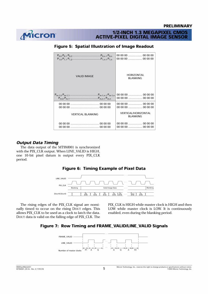
sive scan. Valid image data is surrounded by horizontalblanking and vertical blanking, as shown in Figure 5.The amount of horizontal blanking and vertical blank-ing is programmable through Reg0x05 and Reg0x06,respectively. LINE_VALID is HIGH during the shadedregion of the figure. FRAME_VALID timing is describedin the next section.
(1311, 1047)
16 black columns
7 black rows
8 black rows (0, 0)
7 black columns
SXGA (1,280 x 1,024)+ 4 pixel boundary for
color correction+ additional active column
+ additional active row= 1,289 x 1,033 active pixels
Pixel(8, 16)
black pixelscolumn readout direction
...
...rowreadoutdirection
GBGBGB
RGRGRG
GBGBGB
RGRGRG
GBGBGB
RGRGRG
GBGBGB
1/2-INCH 1.3 MEGAPIXEL CMOSACTIVE-PIXEL DIGITAL IMAGE SENSORPRELIMINARY
09005aef80a3e031 Micron Technology, Inc., reserves the right to change products or specifications without notice.MT9M001_DS.fm - Rev. A 11/03 EN 5 ©2003 Micron Technology, Inc.
Figure 5: Spatial Illustration of Image Readout
Output Data TimingThe data output of the MT9M001 is synchronized
with the PIX_CLK output. When LINE_VALID is HIGH,one 10-bit pixel datum is output every PIX_CLKperiod.
Figure 6: Timing Example of Pixel Data
The rising edges of the PIX_CLK signal are nomi-nally timed to occur on the rising DOUT edges. Thisallows PIX_CLK to be used as a clock to latch the data.DOUT data is valid on the falling edge of PIX_CLK. The
PIX_CLK is HIGH while master clock is HIGH and thenLOW while master clock is LOW. It is continuouslyenabled, even during the blanking period.
Figure 7: Row Timing and FRAME_VALID/LINE_VALID Signals
P0,0 P0,1 P0,2.....................................P0,n-1 P0,nP1,0 P1,1 P1,2.....................................P1,n-1 P1,n
00 00 00 .................. 00 00 0000 00 00 .................. 00 00 00
Pm-1,0 Pm-1,1.....................................Pm-1,n-1 Pm-1,nPm,0 Pm,1.....................................Pm,n-1 Pm,n
00 00 00 .................. 00 00 0000 00 00 .................. 00 00 00
00 00 00 .................. 00 00 0000 00 00 .................. 00 00 00
00 00 00 .................. 00 00 0000 00 00 .................. 00 00 00
00 00 00 ..................................... 00 00 0000 00 00 ..................................... 00 00 00
00 00 00 ..................................... 00 00 0000 00 00 ..................................... 00 00 00
VALID IMAGE HORIZONTALBLANKING
VERTICAL BLANKING VERTICAL/HORIZONTALBLANKING
LINE_VALID
PIX_CLK
DOUT9-DOUT0
. . . .
. . . .
. . . .
. . . .
P0(9:0) P1(9:0) P2(9:0) P3(9:0) P4(9:0) Pn-1(9:0) Pn(9:0)
Valid Image DataBlanking Blanking
P1 A Q A Q A P2
. . .
. . .
. . .Number of master clocks
FRAME_VALID
LINE_VALID
1/2-INCH 1.3 MEGAPIXEL CMOSACTIVE-PIXEL DIGITAL IMAGE SENSORPRELIMINARY
09005aef80a3e031 Micron Technology, Inc., reserves the right to change products or specifications without notice.MT9M001_DS.fm - Rev. A 11/03 EN 6 ©2003 Micron Technology, Inc.
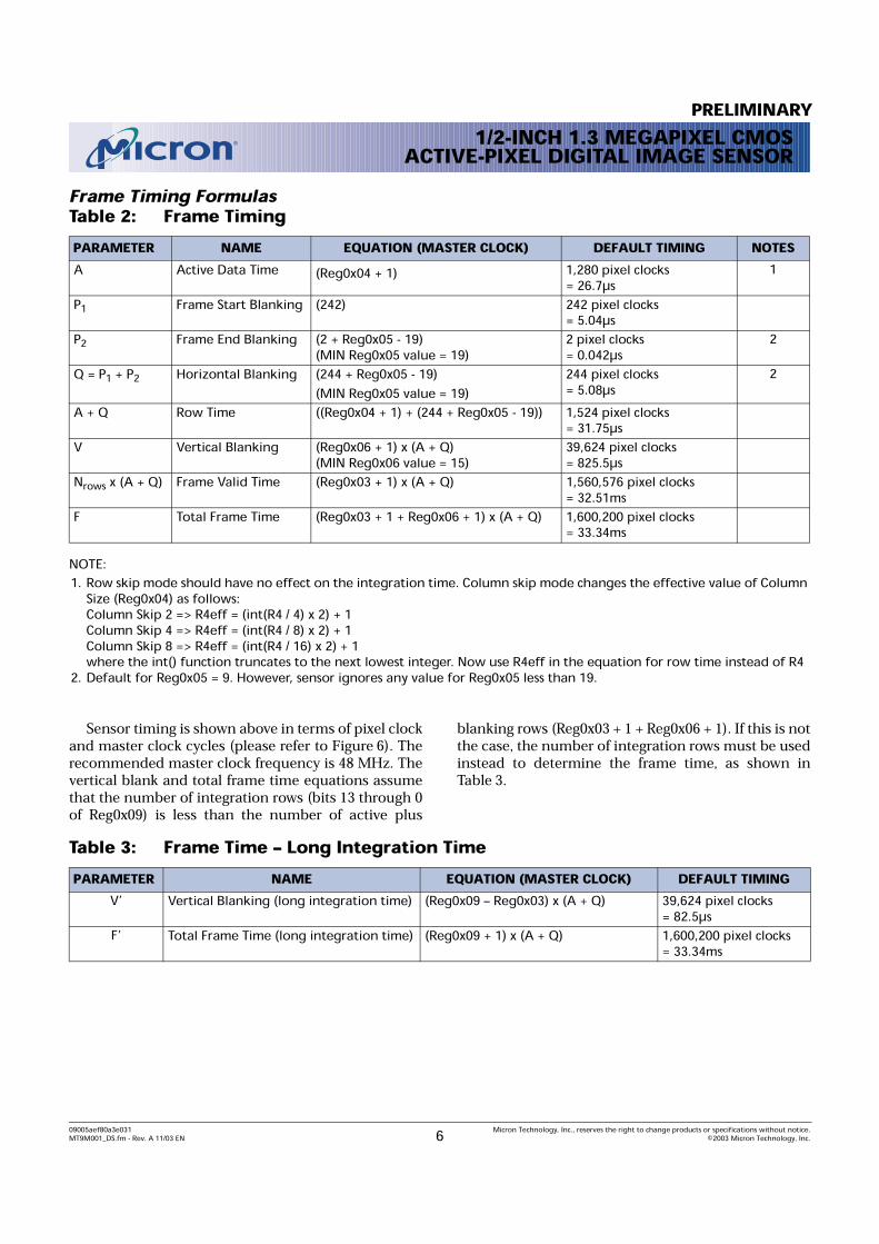
Frame Timing Formulas
NOTE:1. Row skip mode should have no effect on the integration time. Column skip mode changes the effective value of Column
Size (Reg0x04) as follows:Column Skip 2 => R4eff = (int(R4 / 4) x 2) + 1Column Skip 4 => R4eff = (int(R4 / 8) x 2) + 1Column Skip 8 => R4eff = (int(R4 / 16) x 2) + 1where the int() function truncates to the next lowest integer. Now use R4eff in the equation for row time instead of R4
2. Default for Reg0x05 = 9. However, sensor ignores any value for Reg0x05 less than 19.
Sensor timing is shown above in terms of pixel clockand master clock cycles (please refer to Figure 6). Therecommended master clock frequency is 48 MHz. Thevertical blank and total frame time equations assumethat the number of integration rows (bits 13 through 0of Reg0x09) is less than the number of active plus
blanking rows (Reg0x03 + 1 + Reg0x06 + 1). If this is notthe case, the number of integration rows must be usedinstead to determine the frame time, as shown inTable 3.
Table 2: Frame TimingPARAMETER NAME EQUATION (MASTER CLOCK) DEFAULT TIMING NOTESA Active Data Time (Reg0x04 + 1) 1,280 pixel clocks
= 26.7µs1
P1 Frame Start Blanking (242) 242 pixel clocks= 5.04µs
P2 Frame End Blanking (2 + Reg0x05 - 19) (MIN Reg0x05 value = 19)
2 pixel clocks= 0.042µs
2
Q = P1 + P2 Horizontal Blanking (244 + Reg0x05 - 19)(MIN Reg0x05 value = 19)
244 pixel clocks= 5.08µs
2
A + Q Row Time ((Reg0x04 + 1) + (244 + Reg0x05 - 19)) 1,524 pixel clocks = 31.75µs
V Vertical Blanking (Reg0x06 + 1) x (A + Q)(MIN Reg0x06 value = 15)
39,624 pixel clocks= 825.5µs
Nrows x (A + Q) Frame Valid Time (Reg0x03 + 1) x (A + Q) 1,560,576 pixel clocks= 32.51ms
F Total Frame Time (Reg0x03 + 1 + Reg0x06 + 1) x (A + Q) 1,600,200 pixel clocks= 33.34ms
Table 3: Frame Time – Long Integration TimePARAMETER NAME EQUATION (MASTER CLOCK) DEFAULT TIMING
V’ Vertical Blanking (long integration time) (Reg0x09 – Reg0x03) x (A + Q) 39,624 pixel clocks = 82.5µs
F’ Total Frame Time (long integration time) (Reg0x09 + 1) x (A + Q) 1,600,200 pixel clocks= 33.34ms
1/2-INCH 1.3 MEGAPIXEL CMOSACTIVE-PIXEL DIGITAL IMAGE SENSORPRELIMINARY
09005aef80a3e031 Micron Technology, Inc., reserves the right to change products or specifications without notice.MT9M001_DS.fm - Rev. A 11/03 EN 7 ©2003 Micron Technology, Inc.
Serial Bus DescriptionRegisters are written to and read from the MT9M001
through the two-wire serial interface bus. The sensor isa two-wire serial interface slave and is controlled bythe two-wire serial interface clock (SCLK), which isdriven by the two-wire serial interface master. Data istransferred into and out through the MT9M001 two-wire serial interface data (SDATA) line. The SDATA lineis pulled up to 3.3V off-chip by a 1.5KΩ resistor. Eitherthe slave or master device can pull the SDATA linedown—the two-wire serial interface protocol deter-mines which device is allowed to pull the SDATA linedown at any given time.
ProtocolThe two-wire serial interface bus defines several dif-
ferent transmission codes, as follows:• a start bit• the slave device eight-bit address • a(an) (no) acknowledge bit• an eight-bit message• a stop bit
SequenceA typical read or write sequence begins by the mas-
ter sending a start bit. After the start bit, the mastersends the slave device's eight-bit address. The last bitof the address determines if the request will be a reador a write, where a “0” indicates a write and a “1” indi-cates a read. The slave device acknowledges its addressby sending an acknowledge bit back to the master.
If the request was a write, the master then transfersthe eight-bit register address to which a write shouldtake place. The slave sends an acknowledge bit to indi-cate that the register address has been received. Themaster then transfers the data eight bits at a time, withthe slave sending an acknowledge bit after each eightbits. The MT9M001 uses 16-bit data for its internal reg-isters, thus requiring two eight-bit transfers to write toone register. After 16 bits are transferred, the registeraddress is automatically incremented, so that the next16 bits are written to the next register address. Themaster stops writing by sending a start or stop bit.
A typical read sequence is executed as follows. Firstthe master sends the write-mode slave address andeight-bit register address, just as in the write request.The master then sends a start bit and the read-modeslave address. The master then clocks out the registerdata eight bits at a time. The master sends an acknowl-
edge bit after each eight-bit transfer. The registeraddress is auto-incremented after every 16 bits istransferred. The data transfer is stopped when themaster sends a no-acknowledge bit.
Bus Idle StateThe bus is idle when both the data and clock lines
are HIGH. Control of the bus is initiated with a startbit, and the bus is released with a stop bit. Only themaster can generate the start and stop bits.
Start BitThe start bit is defined as a HIGH-to-LOW transition
of the data line while the clock line is HIGH.
Stop BitThe stop bit is defined as a LOW-to-HIGH transition
of the data line while the clock line is HIGH.
Slave AddressThe eight-bit address of a two-wire serial interface
device consists of seven bits of address and 1 bit ofdirection. A “0” in the LSB (least significant bit) of theaddress indicates write mode, and a “1” indicates readmode.
Data Bit TransferOne data bit is transferred during each clock pulse.
The serial interface clock pulse is provided by the mas-ter. The data must be stable during the HIGH period ofthe two-wire serial interface clock—it can only changewhen the serial clock is LOW. Data is transferred eightbits at a time, followed by an acknowledge bit.
Acknowledge BitThe master generates the acknowledge clock pulse.
The transmitter (which is the master when writing, orthe slave when reading) releases the data line, and thereceiver indicates an acknowledge bit by pulling thedata line LOW during the acknowledge clock pulse.
No-Acknowledge BitThe no-acknowledge bit is generated when the data
line is not pulled down by the receiver during theacknowledge clock pulse. A no-acknowledge bit isused to terminate a read sequence.
1/2-INCH 1.3 MEGAPIXEL CMOSACTIVE-PIXEL DIGITAL IMAGE SENSORPRELIMINARY
09005aef80a3e031 Micron Technology, Inc., reserves the right to change products or specifications without notice.MT9M001_DS.fm - Rev. A 11/03 EN 8 ©2003 Micron Technology, Inc.
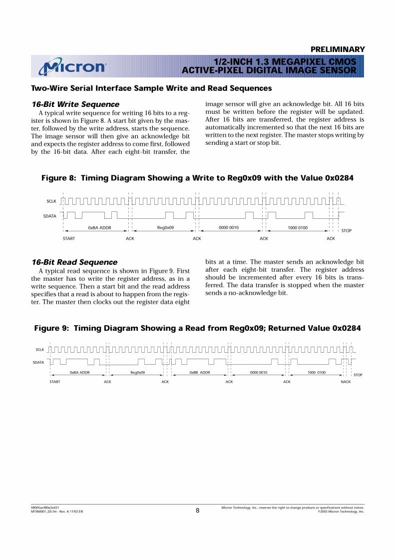
Two-Wire Serial Interface Sample Write and Read Sequences16-Bit Write Sequence
A typical write sequence for writing 16 bits to a reg-ister is shown in Figure 8. A start bit given by the mas-ter, followed by the write address, starts the sequence.The image sensor will then give an acknowledge bitand expects the register address to come first, followedby the 16-bit data. After each eight-bit transfer, the
image sensor will give an acknowledge bit. All 16 bitsmust be written before the register will be updated.After 16 bits are transferred, the register address isautomatically incremented so that the next 16 bits arewritten to the next register. The master stops writing bysending a start or stop bit.
Figure 8: Timing Diagram Showing a Write to Reg0x09 with the Value 0x0284
16-Bit Read SequenceA typical read sequence is shown in Figure 9. First
the master has to write the register address, as in awrite sequence. Then a start bit and the read addressspecifies that a read is about to happen from the regis-ter. The master then clocks out the register data eight
bits at a time. The master sends an acknowledge bitafter each eight-bit transfer. The register addressshould be incremented after every 16 bits is trans-ferred. The data transfer is stopped when the mastersends a no-acknowledge bit.
Figure 9: Timing Diagram Showing a Read from Reg0x09; Returned Value 0x0284
SCLK
SDATA
START ACK
0xBA ADDR
ACK ACK ACKSTOPReg0x09 1000 01000000 0010
SCLK
SDATA
START ACK
0xBA ADDR 0xBB ADDR 0000 0010Reg0x09
ACK ACK ACKSTOP1000 0100
NACK
1/2-INCH 1.3 MEGAPIXEL CMOSACTIVE-PIXEL DIGITAL IMAGE SENSORPRELIMINARY
09005aef80a3e031 Micron Technology, Inc., reserves the right to change products or specifications without notice.MT9M001_DS.fm - Rev. A 11/03 EN 9 ©2003 Micron Technology, Inc.
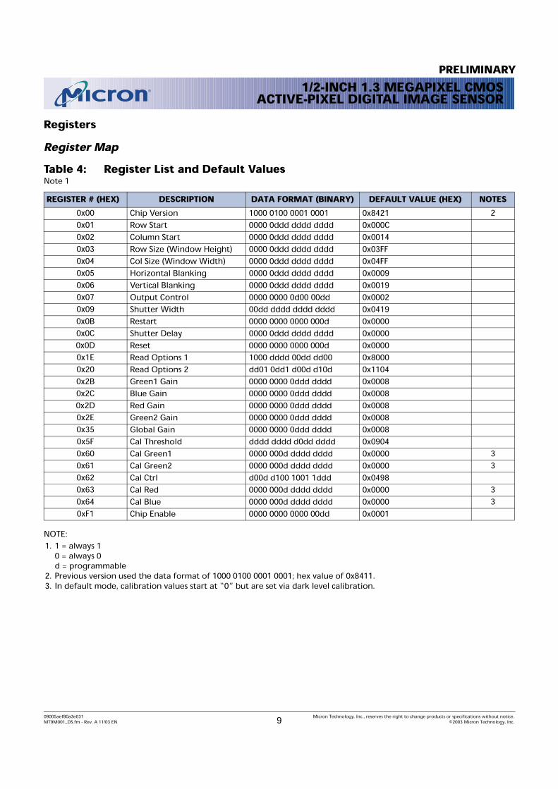
RegistersRegister Map
NOTE:1. 1 = always 1
0 = always 0d = programmable
2. Previous version used the data format of 1000 0100 0001 0001; hex value of 0x8411.3. In default mode, calibration values start at “0” but are set via dark level calibration.
Table 4: Register List and Default ValuesNote 1REGISTER # (HEX) DESCRIPTION DATA FORMAT (BINARY) DEFAULT VALUE (HEX) NOTES
0x00 Chip Version 1000 0100 0001 0001 0x8421 20x01 Row Start 0000 0ddd dddd dddd 0x000C0x02 Column Start 0000 0ddd dddd dddd 0x00140x03 Row Size (Window Height) 0000 0ddd dddd dddd 0x03FF0x04 Col Size (Window Width) 0000 0ddd dddd dddd 0x04FF0x05 Horizontal Blanking 0000 0ddd dddd dddd 0x00090x06 Vertical Blanking 0000 0ddd dddd dddd 0x00190x07 Output Control 0000 0000 0d00 00dd 0x00020x09 Shutter Width 00dd dddd dddd dddd 0x04190x0B Restart 0000 0000 0000 000d 0x00000x0C Shutter Delay 0000 0ddd dddd dddd 0x00000x0D Reset 0000 0000 0000 000d 0x00000x1E Read Options 1 1000 dddd 00dd dd00 0x80000x20 Read Options 2 dd01 0dd1 d00d d10d 0x11040x2B Green1 Gain 0000 0000 0ddd dddd 0x00080x2C Blue Gain 0000 0000 0ddd dddd 0x00080x2D Red Gain 0000 0000 0ddd dddd 0x00080x2E Green2 Gain 0000 0000 0ddd dddd 0x00080x35 Global Gain 0000 0000 0ddd dddd 0x00080x5F Cal Threshold dddd dddd d0dd dddd 0x09040x60 Cal Green1 0000 000d dddd dddd 0x0000 30x61 Cal Green2 0000 000d dddd dddd 0x0000 30x62 Cal Ctrl d00d d100 1001 1ddd 0x04980x63 Cal Red 0000 000d dddd dddd 0x0000 30x64 Cal Blue 0000 000d dddd dddd 0x0000 30xF1 Chip Enable 0000 0000 0000 00dd 0x0001

1/2-INCH 1.3 MEGAPIXEL CMOSACTIVE-PIXEL DIGITAL IMAGE SENSORPRELIMINARY
09005aef80a3e031 Micron Technology, Inc., reserves the right to change products or specifications without notice.MT9M001_DS.fm - Rev. A 11/03 EN 10 ©2003 Micron Technology, Inc.
Table 5: Register DescriptionREGISTER BIT DESCRIPTIONChip ID
0x00 0–15 This register is read-only and gives the chip identification number: 0x8421.Window ControlThese registers control the size of the window.
0x01 0–10 First row to be read out—default = 0x000C (12).0x02 0–10 First column to be read out—default = 0x0014 (20).
Register value must be an even number.0x03 0–10 Window height (number of rows - 1)—default = 0x03FF (1023).
Minimum value for 0x03 = 0x0002.0x04 0–10 Window width (number of columns - 1)—default = 0x04FF (1279).
Register value must be an odd number.Minumum value for 0x04 = 0x0003.
Blanking ControlThese registers control the blanking time in a row (called column fill-in or horizontal blanking) and between frames (vertical blanking). Horizontal blanking is specified in terms of pixel clocks. Vertical blanking is specified in terms of row readout times. The actual imager timing can be calculated using Table 2, Frame Timing, on page 6.
0x05 0–10 Horizontal Blanking—default = 0x0009 (9 pixels).0x06 0–10 Vertical Blanking—default = 0x0019 (25 rows).
Output ControlThis register controls various features of the output format for the sensor.
0x07 0 Synchronize changes (copied to Reg0xF1, bit1).0 = normal operation. Update changes to registers that affect image brightness (integration time, integration delay, gain, horizontal blanking and vertical blanking, window size, row/column skip or row mirror) at the next frame boundary. The “frame boundary” is 8 row_times before the rising edge of FRAME_VALID. (If “Show Dark Rows” is set, it will be coincident with the rising edge of FRAME_VALID.)1 = do not update any changes to these settings until this bit is returned to “0.”
1 Chip Enable (copied to Reg0xF1, bit0).1 = normal operation.0 = stop sensor readout. When this is returned to “1,” sensor readout restarts at the starting row in a new frame. The digital power consumption can then also be reduced to less than 5uA by turning off the master clock.
2 Reserved—default is 0; set to zero at all times.3 Reserved—default is 0; set to zero at all times.6 Override pixel data.
0 = normal operation.1 = output programmed test data (see Reg0x32). First valid columns will output contents of test data register; second columns will output inverted data. Third columns will output noninverted data, fourth inverted, etc.

1/2-INCH 1.3 MEGAPIXEL CMOSACTIVE-PIXEL DIGITAL IMAGE SENSORPRELIMINARY
09005aef80a3e031 Micron Technology, Inc., reserves the right to change products or specifications without notice.MT9M001_DS.fm - Rev. A 11/03 EN 11 ©2003 Micron Technology, Inc.
Pixel Integration ControlThese registers (along with the window sizing and blanking registers) control the integration time for the pixels. The actual total integration time (tINT) is:
tINT = Reg0x09 x row time - overhead time - reset delay, where:Row time = ((Reg0x04 + 1) + 244 + Reg0x05 - 19) pixel clock periodsOverhead time = 180 pixel clock periods
Reset delay = 4 x Reg0x0C pixel clock periodsIf the value in Reg0x0C exceeds (row time - 548)/4 pixel clock cycles, the row time will be extended by (4 x Reg0x0C - (row time - 548)) pixel clock cycles.In this expression, the row time term, Reg0x09 x ((number of columns) + 244 + horizontal blanking register - 19), corresponds to the number of rows integrated. The overhead time (180 pixel clocks) is the overhead time between the READ cycle and the RESET cycle, and the final term is the effect of the reset delay. Typically, the value of Reg0x09 is limited to the number of rows per frame (which includes vertical blanking rows) such that the frame rate is not affected by the integration time. If Reg0x09 is increased beyond the total number of rows per frame, the MT9M001 will add additional blanking rows as needed. A second constraint is that tINT must be adjusted to avoid banding in the image from light flicker. Under 60Hz flicker, this means tINT must be a multiple of 1/120 of a second. Under 50Hz flicker, tINT must be a multiple of 1/100 of a second.
0x09 0–13 Number of rows of integration—default = 0x0419 (1049).0x0C 0–10 Shutter delay—default = 0x0000 (0). This is the number of master clocks times four that the timing
and control logic waits before asserting the reset for a given row.Frame Restart
0x0B 0 Setting bit 0 to “1” of Reg0x0B will cause the sensor to abandon the readout of the current frame and restart from the first row. This register automatically resets itself to 0x0000 after the frame restart. The first frame after this event is considered to be a "bad frame" (see description for Reg0x20, bit0).
Reset0x0D 0 This register is used to reset the sensor to its default, power-up state. To put the MT9M001 in reset
mode first write a “1” into bit 0 of this register, then write a “0” into bit 0 to resume operation.Read Mode 1In read mode 1, this register is used to control many aspects of the readout of the sensor.
Table 5: Register Description (continued)REGISTER BIT DESCRIPTION
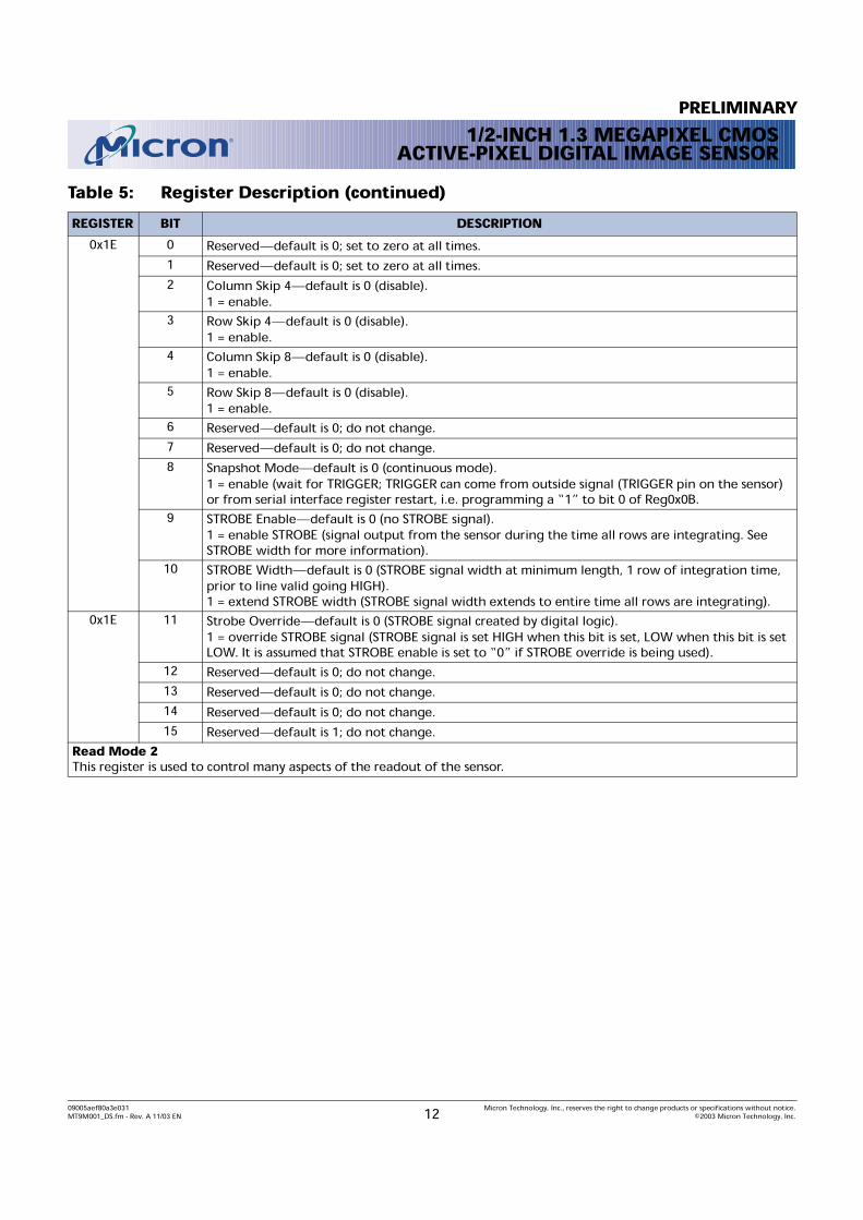
1/2-INCH 1.3 MEGAPIXEL CMOSACTIVE-PIXEL DIGITAL IMAGE SENSORPRELIMINARY
09005aef80a3e031 Micron Technology, Inc., reserves the right to change products or specifications without notice.MT9M001_DS.fm - Rev. A 11/03 EN 12 ©2003 Micron Technology, Inc.
0x1E 0 Reserved—default is 0; set to zero at all times.1 Reserved—default is 0; set to zero at all times.2 Column Skip 4—default is 0 (disable).
1 = enable.3 Row Skip 4—default is 0 (disable).
1 = enable.4 Column Skip 8—default is 0 (disable).
1 = enable.5 Row Skip 8—default is 0 (disable).
1 = enable.6 Reserved—default is 0; do not change.7 Reserved—default is 0; do not change.8 Snapshot Mode—default is 0 (continuous mode).
1 = enable (wait for TRIGGER; TRIGGER can come from outside signal (TRIGGER pin on the sensor) or from serial interface register restart, i.e. programming a “1” to bit 0 of Reg0x0B.
9 STROBE Enable—default is 0 (no STROBE signal).1 = enable STROBE (signal output from the sensor during the time all rows are integrating. See STROBE width for more information).
10 STROBE Width—default is 0 (STROBE signal width at minimum length, 1 row of integration time, prior to line valid going HIGH).1 = extend STROBE width (STROBE signal width extends to entire time all rows are integrating).
0x1E 11 Strobe Override—default is 0 (STROBE signal created by digital logic).1 = override STROBE signal (STROBE signal is set HIGH when this bit is set, LOW when this bit is set LOW. It is assumed that STROBE enable is set to “0” if STROBE override is being used).
12 Reserved—default is 0; do not change.13 Reserved—default is 0; do not change.14 Reserved—default is 0; do not change.15 Reserved—default is 1; do not change.
Read Mode 2This register is used to control many aspects of the readout of the sensor.
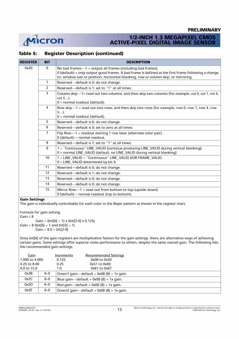
Table 5: Register Description (continued)REGISTER BIT DESCRIPTION
1/2-INCH 1.3 MEGAPIXEL CMOSACTIVE-PIXEL DIGITAL IMAGE SENSORPRELIMINARY
09005aef80a3e031 Micron Technology, Inc., reserves the right to change products or specifications without notice.MT9M001_DS.fm - Rev. A 11/03 EN 13 ©2003 Micron Technology, Inc.
0x20 0 No bad frames—1 = output all frames (including bad frames).0 (default) = only output good frames. A bad frame is defined as the first frame following a change to: window size or position, horizontal blanking, row or column skip, or mirroring.
1 Reserved—default is 0; do not change.2 Reserved—default is 1; set to “1” at all times.3 Column skip—1= read out two columns, and then skip two columns (for example, col 0, col 1, col 4,
col 5…).0 = normal readout (default).
4 Row skip—1 = read out two rows, and then skip two rows (for example, row 0, row 1, row 4, row 5…).0 = normal readout (default).
5 Reserved—default is 0; do not change.6 Reserved—default is 0; set to zero at all times.7 Flip Row—1 = readout starting 1 row later (alternate color pair).
0 (default) = normal readout.8 Reserved—default is 1; set to “1” at all times.9 1 = "Continuous" LINE_VALID (continue producing LINE_VALID during vertical blanking).
0 = normal LINE_VALID (default, no LINE_VALID during vertical blanking).10 1 = LINE_VALID = "Continuous" LINE_VALID XOR FRAME_VALID.
0 = LINE_VALID determined by bit 9.11 Reserved—default is 0; do not change.12 Reserved—default is 1; do not change.13 Reserved—default is 0; do not change.14 Reserved—default is 0; do not change.15 Mirror Row—1 = read out from bottom to top (upside down).
0 (default) = normal readout (top to bottom).Gain SettingsThe gain is individually controllable for each color in the Bayer pattern as shown in the register chart.Formula for gain setting:Gain ≤ 8
Gain = (bit[6] + 1) x (bit[5-0] x 0.125)Gain > 8 (bit[6] = 1 and bit[5] = 1)
Gain = 8.0 + bit[2-0]Since bit[6] of the gain registers are multiplicative factors for the gain settings, there are alternative ways of achieving certain gains. Some settings offer superior noise performance to others, despite the same overall gain. The following lists the recommended gain settings:
Gain Increments Recommended Settings1.000 to 4.000 0.125 0x08 to 0x204.25 to 8.00 0.25 0x51 to 0x609.0 to 15.0 1.0 0x61 to 0x67
0x2B 6–0 Green1 gain—default = 0x08 (8) = 1x gain.0x2C 6–0 Blue gain—default = 0x08 (8) = 1x gain.0x2D 6–0 Red gain—default = 0x08 (8) = 1x gain.0x2E 6–0 Green2 gain—default = 0x08 (8) = 1x gain.
Table 5: Register Description (continued)REGISTER BIT DESCRIPTION

1/2-INCH 1.3 MEGAPIXEL CMOSACTIVE-PIXEL DIGITAL IMAGE SENSORPRELIMINARY
09005aef80a3e031 Micron Technology, Inc., reserves the right to change products or specifications without notice.MT9M001_DS.fm - Rev. A 11/03 EN 14 ©2003 Micron Technology, Inc.
0x35 6–0 Global gain—default = 0x08 (8) = 1x gain. This register can be used to set all four gains at once. When read, it will return the value stored in Reg0x2B.
Black level CalibrationThese registers are used in the black level calibration. Their functionality is described in detail in the next section.
0x5F 5–0 Thres_lo—Lower threshold for black level in ADC LSBs—default = 000100.7 1 = override automatic Thres_hi and Thres_lo adjust (Thres_hi always = bits 14–8; Thres_lo always =
bits 5–0).Default = 0 = Automatic Thres_hi and Thres_lo adjustment.
14-8 Thres_hi—Maximum allowed black level in ADC LSBs (default = Thres_lo + 5).Black level maximum is set to this value when bit 7 = 1; black level maximum is reset to this value after every black level average restart if bit 15 = 1 and bit 7 = 0.
15 No gain dependence.1 = Thres_lo is set by the programmed value of bits 5–0, Thres_hi is reset to the programmed value (bits 14–8) after every black level average restart.0 = Thres_lo and Thres_hi are set automatically, as described above.
0x60 8–0 Cal Green1—analog offset correction value for Green 1, bits 0–7 sets magnitude, bit 8 set sign. 2’scomplement, if bit 8 = 1, Offset = bits [0-7] - 256.0 = positive.1 = negative.
0x61 8–0 Cal Green2—analog offset correction value for Green 2, bits 0–7 sets magnitude, bit 8 set sign.0 = positive.1 = negative.
0x62
0x62
0 Manual override of black level correction.1 = override automatic black level correction with programmed values.0 = normal operation (default).
2–1 Force/disable black level calibration.00 = apply black level calibration during ADC operation only (default).10 = apply black level calibration continuously.X1= disable black level correction (Offset Correction Voltage = 0.0V).(In this case, no black level correction is possible).
4–3 Reserved—default is 1; do not change.6–5 Reserved—default is 0; do not change.7 Reserved—default is 1; do not change.
9–8 Reserved—default is 0; do not change.10 Reserved—default is 1; do not change.11 1 = do not reset the upper threshold after a black level recalculation sweep.
0 = reset the upper threshold after a black level recalculation sweep (default).12 1 = start a new running digitally filtered average for the black level (this is internally reset to “0”
immediately), and do a rapid sweep to find the new starting point.0 = normal operation (default).
14–3 Reserved—default is 0; set to zero at all times.15 1 = do not perform the rapid black level sweep on new gain settings.
0 = normal operation.0x63 8–0 Cal Red—analog offset correction value for Red, bits 0–7 sets magnitude, bit 8 set sign. 2’s
complement, if bit 8 = 1, Offset = bits [0-7] - 256.0 = positive.1 = negative.
Table 5: Register Description (continued)REGISTER BIT DESCRIPTION

1/2-INCH 1.3 MEGAPIXEL CMOSACTIVE-PIXEL DIGITAL IMAGE SENSORPRELIMINARY
09005aef80a3e031 Micron Technology, Inc., reserves the right to change products or specifications without notice.MT9M001_DS.fm - Rev. A 11/03 EN 15 ©2003 Micron Technology, Inc.
0x64 8–0 Cal Blue—analog offset correction value for Blue, bits 0–7 sets magnitude, bit 8 set sign. 2’scomplement, if bit 8 = 1, Offset = bits [0-7] - 256.0 = positive.1 = negative.
Chip Enable and Two-wire serial interface write synchronize.0xF1 0 Mirrors the functionality of Reg0x07 bit1 (Chip Enable).
1 = normal operation.0 = stop sensor readout; when this is returned to “1,” sensor readout restarts at the starting row in a new frame.
1 Mirrors the functionality of Reg0x07 bit0 (Synchronize changes).0 = normal operation, update changes to registers that affect image brightness (integration time, integration delay, gain, horizontal blanking and vertical blanking, window size, row/column skip, or row/column mirror) at the next frame boundary.1 = do not update any changes to these settings until this bit is returned to “0.”
Table 5: Register Description (continued)REGISTER BIT DESCRIPTION
1/2-INCH 1.3 MEGAPIXEL CMOSACTIVE-PIXEL DIGITAL IMAGE SENSORPRELIMINARY
09005aef80a3e031 Micron Technology, Inc., reserves the right to change products or specifications without notice.MT9M001_DS.fm - Rev. A 11/03 EN 16 ©2003 Micron Technology, Inc.
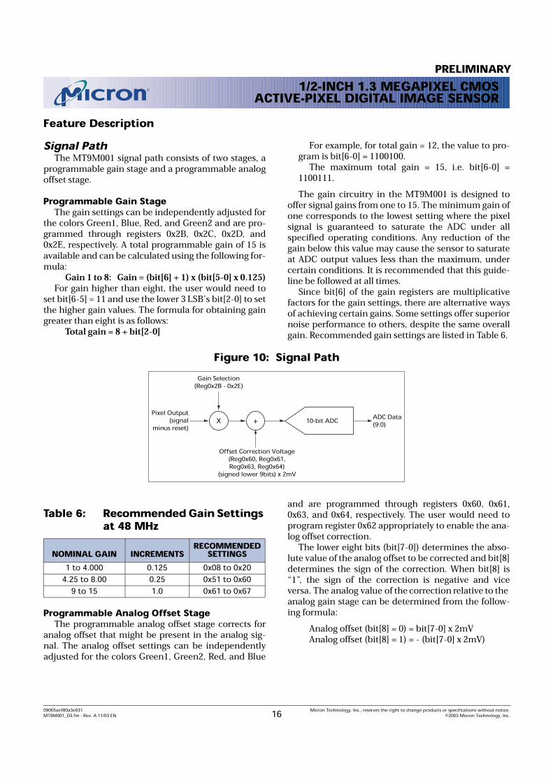
Feature DescriptionSignal Path
The MT9M001 signal path consists of two stages, aprogrammable gain stage and a programmable analogoffset stage.Programmable Gain Stage
The gain settings can be independently adjusted forthe colors Green1, Blue, Red, and Green2 and are pro-grammed through registers 0x2B, 0x2C, 0x2D, and0x2E, respectively. A total programmable gain of 15 isavailable and can be calculated using the following for-mula:
Gain 1 to 8: Gain = (bit[6] + 1) x (bit[5-0] x 0.125)For gain higher than eight, the user would need to
set bit[6-5] = 11 and use the lower 3 LSB’s bit[2-0] to setthe higher gain values. The formula for obtaining gaingreater than eight is as follows:
Total gain = 8 + bit[2-0]
For example, for total gain = 12, the value to pro-gram is bit[6-0] = 1100100.
The maximum total gain = 15, i.e. bit[6-0] =1100111.The gain circuitry in the MT9M001 is designed to
offer signal gains from one to 15. The minimum gain ofone corresponds to the lowest setting where the pixelsignal is guaranteed to saturate the ADC under allspecified operating conditions. Any reduction of thegain below this value may cause the sensor to saturateat ADC output values less than the maximum, undercertain conditions. It is recommended that this guide-line be followed at all times.
Since bit[6] of the gain registers are multiplicativefactors for the gain settings, there are alternative waysof achieving certain gains. Some settings offer superiornoise performance to others, despite the same overallgain. Recommended gain settings are listed in Table 6.
Figure 10: Signal Path
Programmable Analog Offset Stage The programmable analog offset stage corrects for
analog offset that might be present in the analog sig-nal. The analog offset settings can be independentlyadjusted for the colors Green1, Green2, Red, and Blue
and are programmed through registers 0x60, 0x61,0x63, and 0x64, respectively. The user would need toprogram register 0x62 appropriately to enable the ana-log offset correction.
The lower eight bits (bit[7-0]) determines the abso-lute value of the analog offset to be corrected and bit[8]determines the sign of the correction. When bit[8] is“1”, the sign of the correction is negative and viceversa. The analog value of the correction relative to the analog gain stage can be determined from the follow-ing formula:
Analog offset (bit[8] = 0) = bit[7-0] x 2mVAnalog offset (bit[8] = 1) = - (bit[7-0] x 2mV)
X +Pixel Output
(signalminus reset)
Offset Correction Voltage(Reg0x60, Reg0x61,Reg0x63, Reg0x64)
(signed lower 9bits) x 2mV
10-bit ADC ADC Data(9:0)
Gain Selection(Reg0x2B - 0x2E)
Table 6: Recommended Gain Settings at 48 MHz
NOMINAL GAIN INCREMENTS RECOMMENDED SETTINGS1 to 4.000 0.125 0x08 to 0x20
4.25 to 8.00 0.25 0x51 to 0x609 to 15 1.0 0x61 to 0x67
1/2-INCH 1.3 MEGAPIXEL CMOSACTIVE-PIXEL DIGITAL IMAGE SENSORPRELIMINARY
09005aef80a3e031 Micron Technology, Inc., reserves the right to change products or specifications without notice.MT9M001_DS.fm - Rev. A 11/03 EN 17 ©2003 Micron Technology, Inc.
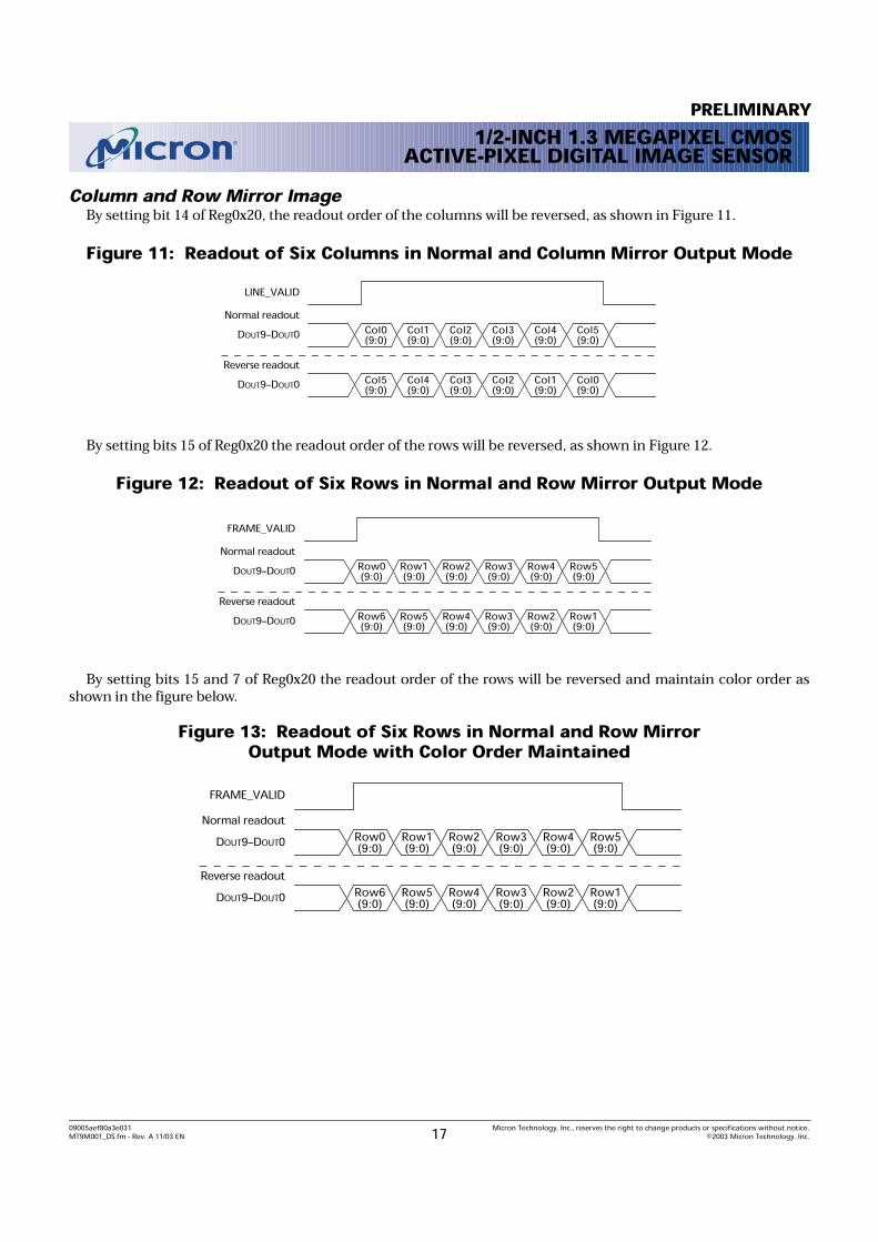
Column and Row Mirror Image By setting bit 14 of Reg0x20, the readout order of the columns will be reversed, as shown in Figure 11.
Figure 11: Readout of Six Columns in Normal and Column Mirror Output Mode
By setting bits 15 of Reg0x20 the readout order of the rows will be reversed, as shown in Figure 12.
Figure 12: Readout of Six Rows in Normal and Row Mirror Output Mode
By setting bits 15 and 7 of Reg0x20 the readout order of the rows will be reversed and maintain color order asshown in the figure below.
Figure 13: Readout of Six Rows in Normal and Row MirrorOutput Mode with Color Order Maintained
DOUT9–DOUT0
LINE_VALIDNormal readout
Col0(9:0) Col1(9:0) Col2(9:0) Col3(9:0) Col4(9:0) Col5(9:0)
DOUT9–DOUT0Reverse readout
Col5(9:0) Col4(9:0) Col3(9:0) Col2(9:0) Col1(9:0) Col0(9:0)
DOUT9–DOUT0
FRAME_VALIDNormal readout
Row0(9:0) Row1(9:0) Row2(9:0) Row3(9:0) Row4(9:0) Row5(9:0)
DOUT9–DOUT0Reverse readout
Row5(9:0)Row6(9:0) Row4(9:0) Row3(9:0) Row2(9:0) Row1(9:0)
DOUT9–DOUT0
FRAME_VALIDNormal readout
Row0(9:0) Row1(9:0) Row2(9:0) Row3(9:0) Row4(9:0) Row5(9:0)
DOUT9–DOUT0Reverse readout
Row5(9:0)Row6(9:0) Row4(9:0) Row3(9:0) Row2(9:0) Row1(9:0)

1/2-INCH 1.3 MEGAPIXEL CMOSACTIVE-PIXEL DIGITAL IMAGE SENSORPRELIMINARY
09005aef80a3e031 Micron Technology, Inc., reserves the right to change products or specifications without notice.MT9M001_DS.fm - Rev. A 11/03 EN 18 ©2003 Micron Technology, Inc.
Column and Row SkipBy setting bit 3 of Reg0x20, only half of the columns
set will be read out. An example is shown in Figure 14.Only columns with bit 1 equal to “0” will be read out(xxxxxxx0x). The row skip works in the same way and
will only read out rows with bit 1 equal to “0.” Row skipmode is enabled by setting bit 4 of Reg0x20. For bothrow and column skips, the number of rows or columnsread out will be half of what is set in Reg0x03 orReg0x04, respectively.
Figure 14: Readout of Eight Pixels in Normal and Column Skip Output Mode
DOUT9–DOUT0
LINE_VALIDNormal readout
G0(9:0) R0(9:0) G1(9:0) R1(9:0) G2(9:0) R2(9:0) G3(9:0) R3(9:0)
DOUT9–DOUT0
LINE_VALIDColumn skip readout
G0(9:0) R0(9:0) G2(9:0) R2(9:0)

1/2-INCH 1.3 MEGAPIXEL CMOSACTIVE-PIXEL DIGITAL IMAGE SENSORPRELIMINARY
09005aef80a3e031 Micron Technology, Inc., reserves the right to change products or specifications without notice.MT9M001_DS.fm - Rev. A 11/03 EN 22 ©2003 Micron Technology, Inc.
Still Image Capture with External Synchronization
In continuous mode video image capture, the TRIG-GER signal should be held LOW or “0.” To capture astill image, the sensor must first be put into snapshotmode by programming a “1” in register 0x1E, bit 8. Insnapshot mode, the sensor waits for a TRIGGER signal(FRAME_VALID, LINE_VALID signals are LOW, pixelclock signal continues). When the TRIGGER signal is
received (active HIGH), one frame is read out (a TRIG-GER signal can also be achieved by programming arestart—for example, program a “1” to bit 0 ofReg0x0B). The reset, readout timing for that frame willbe the same as for a continuous frame with similar reg-ister settings; the only difference is that only one frameis read out. General timing for the snapshot mode isshown in Figure 16.
Figure 16: General Timing for Snapshot Mode
LINE_VALID SignalBy setting bit 9 and 10 of Reg0x20 the line valid sig-
nal can get three different output formats. The formatsare shown when reading out four rows and two vertical
blanking rows (Figure 17). In the last format, theLINE_VALID signal is the XOR between the continu-ously LINE_VALID signal and the FRAME_VALID sig-nal.
Figure 17: Different LINE_VALID Formats
TRIGGERReset Row 1
Reset Row
Reset Row x
STROBE
Readout
MAX strobe length (all rows integrating)
MIN strobe length (1 row time)
DefaultFRAME_VALID
LINE_VALID
ContinuouslyFRAME_VALID
LINE_VALID
XORFRAME_VALID
LINE_VALID
1/2-INCH 1.3 MEGAPIXEL CMOSACTIVE-PIXEL DIGITAL IMAGE SENSORPRELIMINARY
09005aef80a3e031 Micron Technology, Inc., reserves the right to change products or specifications without notice.MT9M001_DS.fm - Rev. A 11/03 EN 23 ©2003 Micron Technology, Inc.
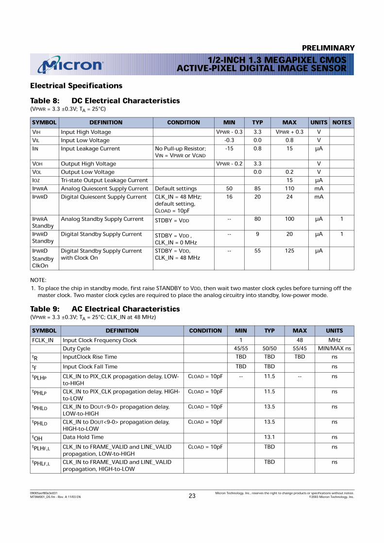
Electrical Specifications
NOTE:1. To place the chip in standby mode, first raise STANDBY to VDD, then wait two master clock cycles before turning off the
master clock. Two master clock cycles are required to place the analog circuitry into standby, low-power mode.
Table 8: DC Electrical Characteristics(VPWR = 3.3 ±0.3V; TA = 25°C)SYMBOL DEFINITION CONDITION MIN TYP MAX UNITS NOTESVIH Input High Voltage VPWR - 0.3 3.3 VPWR + 0.3 VVIL Input Low Voltage -0.3 0.0 0.8 VIIN Input Leakage Current No Pull-up Resistor;
VIN = VPWR or VGND-15 0.8 15 µA
VOH Output High Voltage VPWR - 0.2 3.3 VVOL Output Low Voltage 0.0 0.2 VIOZ Tri-state Output Leakage Current 15 µAIPWRA Analog Quiescent Supply Current Default settings 50 85 110 mAIPWRD Digital Quiescent Supply Current CLK_IN = 48 MHz;
default setting, CLOAD = 10pF
16 20 24 mA
IPWRAStandby
Analog Standby Supply Current STDBY = VDD -- 80 100 µA 1
IPWRDStandby
Digital Standby Supply Current STDBY = VDD ,CLK_IN = 0 MHz
-- 9 20 µA 1
IPWRDStandby ClkOn
Digital Standby Supply Current with Clock On
STDBY = VDD,CLK_IN = 48 MHz
-- 55 125 µA
Table 9: AC Electrical Characteristics(VPWR = 3.3 ±0.3V; TA = 25°C; CLK_IN at 48 MHz)SYMBOL DEFINITION CONDITION MIN TYP MAX UNITSFCLK_IN Input Clock Frequency Clock 1 48 MHz
Duty Cycle 45/55 50/50 55/45 MIN/MAX nstR InputClock Rise Time TBD TBD TBD nstF Input Clock Fall Time TBD TBD nstPLHP CLK_IN to PIX_CLK propagation delay, LOW-
to-HIGHCLOAD = 10pF -- 11.5 -- ns
tPHLP CLK_IN to PIX_CLK propagation delay, HIGH-to-LOW
CLOAD = 10pF 11.5 ns
tPHLD CLK_IN to DOUT<9-0> propagation delay, LOW-to-HIGH
CLOAD = 10pF 13.5 ns
tPHLD CLK_IN to DOUT<9-0> propagation delay, HIGH-to-LOW
CLOAD = 10pF 13.5 ns
tOH Data Hold Time 13.1 nstPLHF,L CLK_IN to FRAME_VALID and LINE_VALID
propagation, LOW-to-HIGHCLOAD = 10pF TBD ns
tPHLF,L CLK_IN to FRAME_VALID and LINE_VALID propagation, HIGH-to-LOW
TBD ns