Lezione Termografia 2017 - uniroma1.itmwl.diet.uniroma1.it/TeAB/Lezione_Termografia_2017.pdf ·...
28
Termografia
Transcript of Lezione Termografia 2017 - uniroma1.itmwl.diet.uniroma1.it/TeAB/Lezione_Termografia_2017.pdf ·...
Termografia
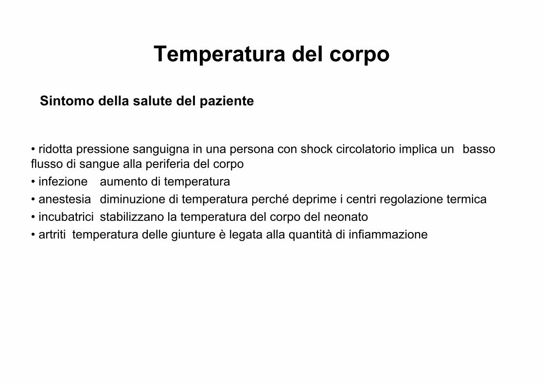
Temperatura del corpo
• ridotta pressione sanguigna in una persona con shock circolatorio implica un bassoflusso di sangue alla periferia del corpo• infezione aumento di temperatura• anestesia diminuzione di temperatura perché deprime i centri regolazione termica• incubatrici stabilizzano la temperatura del corpo del neonato• artriti temperatura delle giunture è legata alla quantità di infiammazione
Sintomo della salute del paziente

Termografia medicaSi basa sulla relazione tra la temperatura superficiale di un corpo e la sua potenza radiante; la temperatura delle varie zone dipende dai processi circolatori o cellulari che si hanno in un particolare punto; mappa della distribuzione della temperatura di un corpo con sensibilità di pochi decimi di grado °C
Applicazioni:tumore al senodisturbi artriticidisturbi circolatori

Immagini

5
0.001
0.002
0.0030.00312
10
Wavelength, µm
15 20
T = 300 K
lm= 9.66 µm
25
20
40
60
80
100%
% T
otal
pow
er
Spec
tral r
adie
nt e
mitt
ance
, W-c
m-2
·mm
-1
Radiazione termica
Spettro della radiazione a temperatura ambiente: 80% della potenza totale si trova nel lontano-molto lontano IR (4÷25 µm)
Massimo della potenza radiante lm=2898/T (µm)
Legge di Stefan-Boltzmann: la potenza radiante totale Wt=esT4 (W/m2) s = 5.67 10-12 W/cm2K4
Legge di Planck
W potenza radiante (W/cm2 µm)l lunghezza d’onda (µm)C1=3.74 104 (W µm4/cm2) C2=1.44 104 (µm K)T temperatura e emissività, (corpo nero e=1)
Corpo nero:assorbe tutta la radiazione incidente ed emette la massima radiazione termica possibile
W (λ) = εC1λ 5
exp(C2 / λT )−1[ ]−1
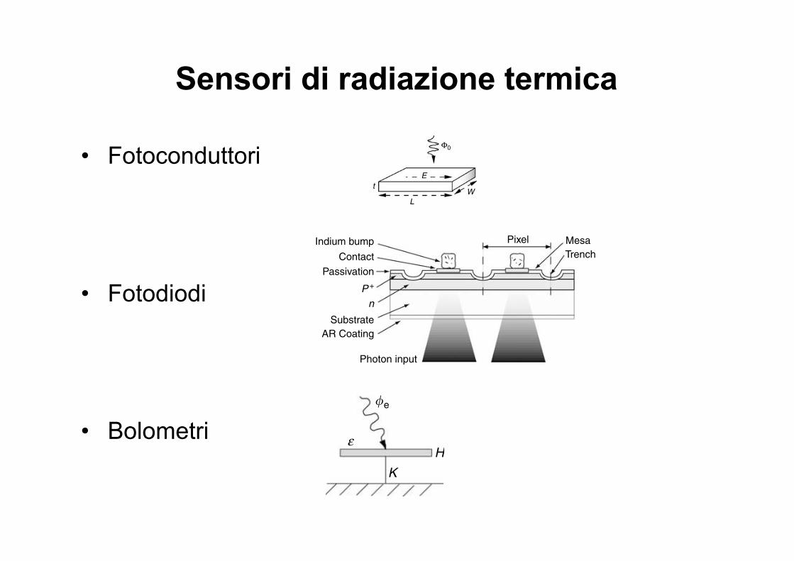
Sensori di radiazione termica
• Fotoconduttori
• Fotodiodi
• Bolometri
3-2 Medical Infrared Imaging
t
L
E
W
Φ0
FIGURE 3.1 Photoconductive detector geometery.
Cur
rent
Voltage
Ligh
tDar
k
FIGURE 3.2 Current–voltage characteristics of a photoconductive detector.
where h is the Planck’s constant, c is the speed of light, and λ is the wavelength of the infrared photon inmicrometers (µm).
Photon detectors respond by elevating an bound electron in a material to a free or conductive state.Two types are photon detectors are produced for the commercial market:
• Photoconductive• Photovoltaic
3.1.1 Photoconductive Detectors
The mechanism of photoconductive detectors is based upon the excitation of bound electrons to a mobilestate where they can move freely through the material. The increase in the number of conductive electrons,n, created by the photon flux, "0 allows more current to flow when the detective element is used in a biascircuit having an electric field E . The photoconductive detector element having dimensions of length L,width W , and thickness t is represented in Figure 3.1.
Figure 3.2 illustrates how the current–voltage characteristics of a photoconductor change with incidentphoton flux (Chapter 4).
The response of a photoconductive detector can be written as:
R = ηqREτ (µn + µp)
EphL(V /W ) (3.2)
where R is the response in volts per Watt, η is the quantum efficiency in electrons per photon, q is thecharge of an electron, R is the resistance of the detector element, τ is the lifetime of a photoexcited electron,and µn and µp are the mobilities of the electrons and holes in the material in volts per square centimeterper second.
Noise in photoconductors is the square root averaged sum of terms from three sources:
• Johnson noise• Thermal generation-recombination• Photon generation-recombination
© 2008 by Taylor & Francis Group, LLC
Infrared Detectors and Detector Arrays 3-3
Indium bump Pixel MesaTrenchContact
Passivation
SubstrateAR Coating
Photon input
P +
n
FIGURE 3.3 Photovoltaic detector structure example for mesa diodes.
Expressions for the total noise and each of the noise terms are given in Equations 3.3 to 3.6
Vnoise =!
V 2Johnson + V 2
phg-r + V 2thg-r (3.3)
VJohnson =√
4kTR (3.4)
Vph g-r =√
ηφ(WL)2qREτ (µn + µp)
L(3.5)
Vth g-r ="
np
n + pτ
#
Wt
L
$
2qRE(µn + µp) (3.6)
The figure of merit for infrared detectors is called D∗. The units of D∗ are cm (Hz)1/2/W, but are mostcommonly referred to as Jones. D∗ is the detector’s signal-to-noise (SNR) ratio, normalized to an area of1 cm2, to a noise bandwidth of 1 Hz, and to a signal level of 1 W at the peak of the detectors response.The equation for D∗ is:
D∗peak = R
Vnoise
√WL (Jones) (3.7)
where W and L are defined in Figure 3.1.A special condition of D∗ for a photoconductor is noted when the noise is dominated by the photon
noise term. This is a condition in which the D∗ is maximum.
D∗blip = λ
2hc
"
η
Eph(3.8)
where “blip” notes background-limited photodetector.
3.1.2 Photovoltaic Detectors
The mechanism of photovoltaic detectors is based on the collection of photoexcited carriers by a diodejunction. Photovoltaic detectors are the most commonly used photon detectors for imaging arrays incurrent production. An example of the structure of detectors in such an array is illustrated in Figure 3.3for a mesa photodiode. Photons are incident from the optically transparent detector substrate side andare absorbed in the n-type material layer. Absorbed photons create a pair of carriers, an electron and ahole. The hole diffuses to the p-type side of the junction creating a photocurrent. A contact on the p-typeside of the junction is connected to an indium bump that mates to an amplifier in a readout circuit wherethe signal is stored and conveyed to a display during each display frame. A common contact is made to
© 2008 by Taylor & Francis Group, LLC
3-6 Medical Infrared Imaging
3.2 Thermal Detectors
Thermal detectors operate by converting the incoming photon flux to heat [3]. The heat input causesthe thermal detector’s temperature to rise and this change in temperature is sensed by a bolometer.A bolometer element operates by changing its resistance as its temperature is changed. A bias circuitacross the bolometer can be used to convert the changing current to a signal output.
The coefficient α is used to compare the sensitivity of different bolometer materials and is given by:
α = 1
Rd
dR
dT(3.18)
where Rd is the resistance of the bolometer element, and dR/dT is the change in resistance per unit changein temperature. Typical values of α are 2 to 3%.
Theoretically, the bolometer structure can be represented as illustrated in Figure 3.6. The rise intemperature due to a heat flux φe is given by:
#T = ηP0
G(1 + ω2τ 2)1/2 (3.19)
where P0 is the radiant power of the signal in watts, G is the thermal conductance (K/W), h is thepercentage of flux absorbed, and ω is the angular frequency of the signal. The bolometer time constant,τ , is determined by:
τ = C
G(3.20)
where C is the heat capacity of detector element.The sensitivity or D∗ of a thermal detector is limited by variations in the detector temperature caused
by fluctuations in the absorption and radiation of heat between the detector element and the background.Sensitive thermal detectors must minimize competing mechanisms for heat loss by the element, namely,convection and conduction.
Convection by air is eliminated by isolating the detector in a vacuum. If the conductive heat losses wereless than those due to radiation, then the limiting D∗ would be given by:
D∗(T , f ) = 2.8 × 10¹⁶
!
ε
T 52 + T 5
1
Jone (3.21)
where T1 is the detector temperature, T2 the background temperature, and ε the value of the detector’semissivity and equally it’s absorption. For the usual case of both the detector and background temperatureat normal ambient, 300 K, the limiting D∗ is 1.8 × 10¹⁰ Jones.
Bolometer operation is constrained by the requirement that the response time of the detector becompatible with the frame rate of the imaging system. Most bolometer cameras operate at a 30 Hz frame
K
H
!e
ε
FIGURE 3.6 Abstract bolometer detector structure, where C is the thermal capacitance, G is the thermalconductance, and ε is the emissivity of the surface. φe represents the energy flux in W/cm2.
© 2008 by Taylor & Francis Group, LLC
Parametri di un rivelatore IR
• NEP
• Detectivity
• DBLIP
• NEDT
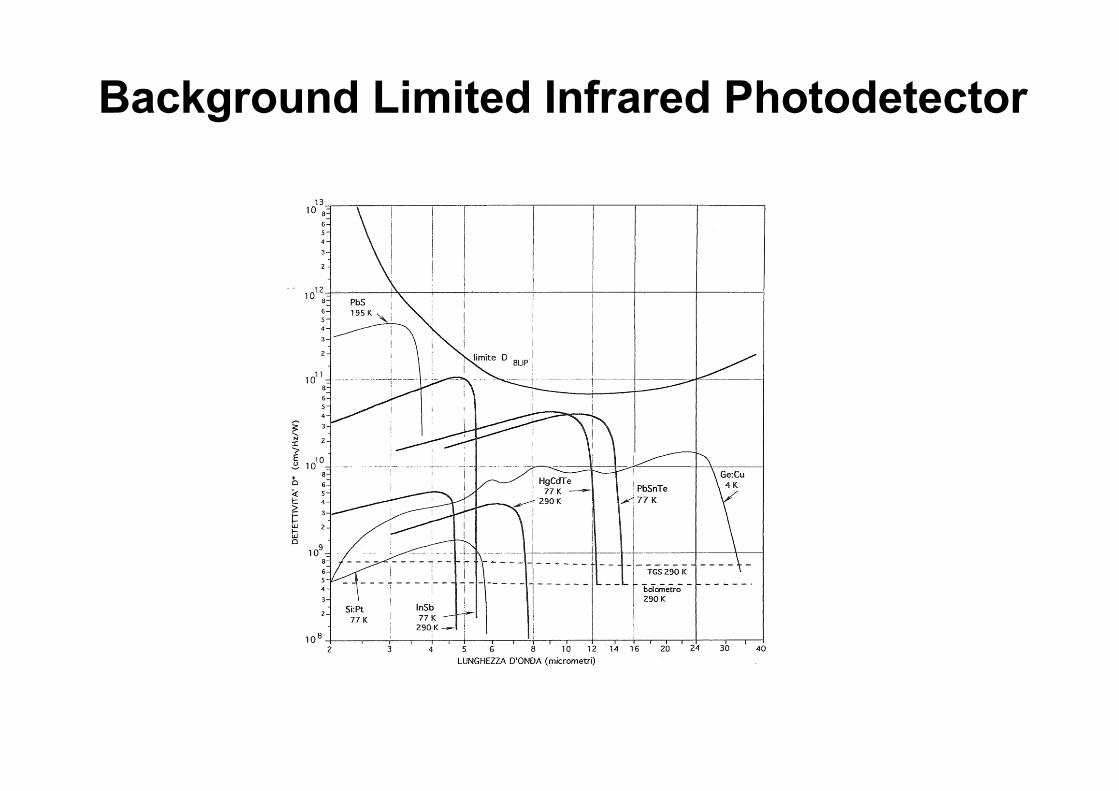
Background Limited Infrared Photodetector

Materiali per rivelatore IR
• CdHgTe (fotodiodi)3-8 Medical Infrared Imaging
10 12 140
1
0.1
0.012 4 6
Wavelength (mm)
Rel
ativ
e re
spon
se (p
er W
att)
8
FIGURE 3.8 Representative spectral response curves for a variety of HgCdTe alloy detectors. Spectral cutoff can bevaried over the SWIR, MWIR, and LWIR regions.
4 5 6 7 8 9 10 11 12 13
107
106
105
104
103
102
101
100
Wavelength (mm)
0 FOV
f/2
R0A
(Ω c
m2 )
FIGURE 3.9 Values of R0A product as a function of wavelength for HgCdTe photodiodes. Note that the R0Aproduct varies slightly with illumination — 0 field-of-view compared with f /2 — especially for shorter-wavelengthdevices.
At 80 K the leakage current of HgCdTe is small enough to provide both MWIR and LWIR detectorsthat can be photon-noise dominated. Figure 3.9 shows the R0A product of representative diodes forwavelengths ranging from 4 to 12 µm.
The versatility of HgCdTe detector material is directly related to being able to grow a broad range ofalloy compositions in order to optimize the response at a particular wavelength. Alloys are usually adjustedto provide response in the 1 to 3 µm short wavelength infrared (SWIR), 3 to 5 µm MWIR, or the 8 to12 µm LWIR spectral regions. Short wavelength detectors can operate uncooled, or with thermoelectriccoolers that have no moving parts. Medium and long wavelength detectors are generally operated at 80 Kusing a cryogenic cooler engine. HgCdTe detectors in 256 × 256, 240 × 320, 480 × 640, and 512 × 640formats are available from a number of vendors.
Quantum well infrared photodetectors (QWIPs) consist of alternating layers of semiconductor materialwith larger and narrower bandgaps [14–20]. This series of alternating semiconductor layers is depositedone layer upon another using an ultrahigh vacuum technique such as molecular beam epitaxy (MBE).Alternating large and narrow bandgap materials give rise to quantum wells that provide bound andquasi-bound states for electrons or holes [1–5].
© 2008 by Taylor & Francis Group, LLC
Infrared Detectors and Detector Arrays 3-9
GaAs AlGaAs
FIGURE 3.10 Quantum wells generate bound states for electrons in the conduction band. The conduction bandsfor a QWIP structure are shown consisting of Alx Ga1−x As barriers and GaAs wells. For a given pair of materialshaving a fixed conduction band offset, the binding energy of an electron in the well can be adjusted by varying thewidth of the well. With an applied bias, photoexcited electrons from the GaAs wells are transported and detected asphotocurrent.
Photon input
Indium bumpContact/grating
Alternating layersGaAs/AlGaAs
n– GaAs contactUndoped GaAs
EtchStop
FIGURE 3.11 Backside illuminated QWIP structure with a top side diffraction grating/contact metal. Normally-incident light is coupled horizontally into the quantum wells by scattering off a diffraction grating located at the topof the focal plane array.
Many simple QWIP structures have used GaAs as the narrow bandgap quantum well material andAlx Ga1−x As as the wide bandgap barrier layers as shown in Figure 3.10. The properties of the QWIP arerelated to the structural design and can be specified by the well width, barrier height, and doping density.In turn, these parameters can be tuned by controlling the cell temperatures of the gallium, aluminum,and arsenic cells as well as the doping cell temperature. The quantum well width (thickness) is governedby the time interval for which the Ga and As cell shutters are left opened. The barrier height is regulatedby the composition of the Alx Ga1−x As layers, which are determined by the relative temperature of the Aland Ga cells. QWIP detectors rely on the absorption of incident radiation within the quantum well andtypically the well material is doped n-type at an approximate level of 5 × 10¹⁷.
The QWIP detectors require that an electric field component of the incident radiation be perpendicularto the layer planes of the device. Imaging arrays use diffraction gratings as shown in Figure 3.11. Inparticular, the latter approach is of practical importance in order to realize two-dimensional detectorarrays. The QWIP focal plane array is a reticulated structure formed by conventional photolithographictechniques. Part of the processing involves placing a two-dimensional metallic grating over the focalplane pixels. The grating metal is typically angled at 45 patterns to reflect incident light obliquely so asto couple the perpendicular component of the electric field into the quantum wells thus producing thephotoexcitation. The substrate material (GaAs) is backside thinned and a chemical/mechanical polish isused to produce a mirrorlike finish on the backside. The front side of the pixels with indium bumps areflip-chip bonded to a readout IC. Light travels through the back side and is unabsorbed during its firstpass through the epilayers; upon scattering with a horizontal propagation component from the gratingsome of it is then absorbed by the quantum wells, photoexciting carriers. An electric field is producedperpendicular to the layers by applying a bias voltage at doped contact layers. The structure then behavesas a photoconductor.
© 2008 by Taylor & Francis Group, LLC
Infrared Detectors and Detector Arrays 3-3
Indium bump Pixel MesaTrenchContact
Passivation
SubstrateAR Coating
Photon input
P +
n
FIGURE 3.3 Photovoltaic detector structure example for mesa diodes.
Expressions for the total noise and each of the noise terms are given in Equations 3.3 to 3.6
Vnoise =!
V 2Johnson + V 2
phg-r + V 2thg-r (3.3)
VJohnson =√
4kTR (3.4)
Vph g-r =√
ηφ(WL)2qREτ (µn + µp)
L(3.5)
Vth g-r ="
np
n + pτ
#
Wt
L
$
2qRE(µn + µp) (3.6)
The figure of merit for infrared detectors is called D∗. The units of D∗ are cm (Hz)1/2/W, but are mostcommonly referred to as Jones. D∗ is the detector’s signal-to-noise (SNR) ratio, normalized to an area of1 cm2, to a noise bandwidth of 1 Hz, and to a signal level of 1 W at the peak of the detectors response.The equation for D∗ is:
D∗peak = R
Vnoise
√WL (Jones) (3.7)
where W and L are defined in Figure 3.1.A special condition of D∗ for a photoconductor is noted when the noise is dominated by the photon
noise term. This is a condition in which the D∗ is maximum.
D∗blip = λ
2hc
"
η
Eph(3.8)
where “blip” notes background-limited photodetector.
3.1.2 Photovoltaic Detectors
The mechanism of photovoltaic detectors is based on the collection of photoexcited carriers by a diodejunction. Photovoltaic detectors are the most commonly used photon detectors for imaging arrays incurrent production. An example of the structure of detectors in such an array is illustrated in Figure 3.3for a mesa photodiode. Photons are incident from the optically transparent detector substrate side andare absorbed in the n-type material layer. Absorbed photons create a pair of carriers, an electron and ahole. The hole diffuses to the p-type side of the junction creating a photocurrent. A contact on the p-typeside of the junction is connected to an indium bump that mates to an amplifier in a readout circuit wherethe signal is stored and conveyed to a display during each display frame. A common contact is made to
© 2008 by Taylor & Francis Group, LLC
• QWIP (fotoconduttori)
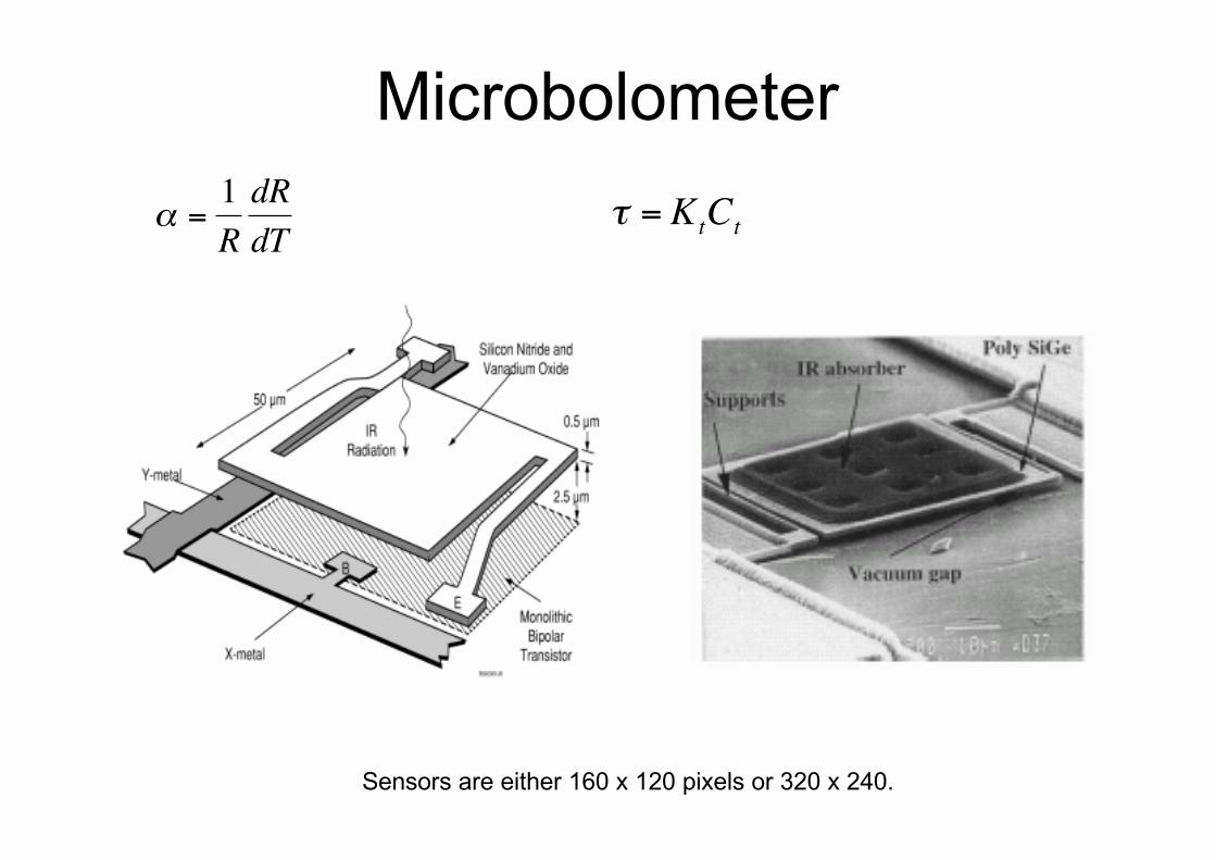
Microbolometer
Sensors are either 160 x 120 pixels or 320 x 240.
€
α =1RdRdT
€
τ = KtCt
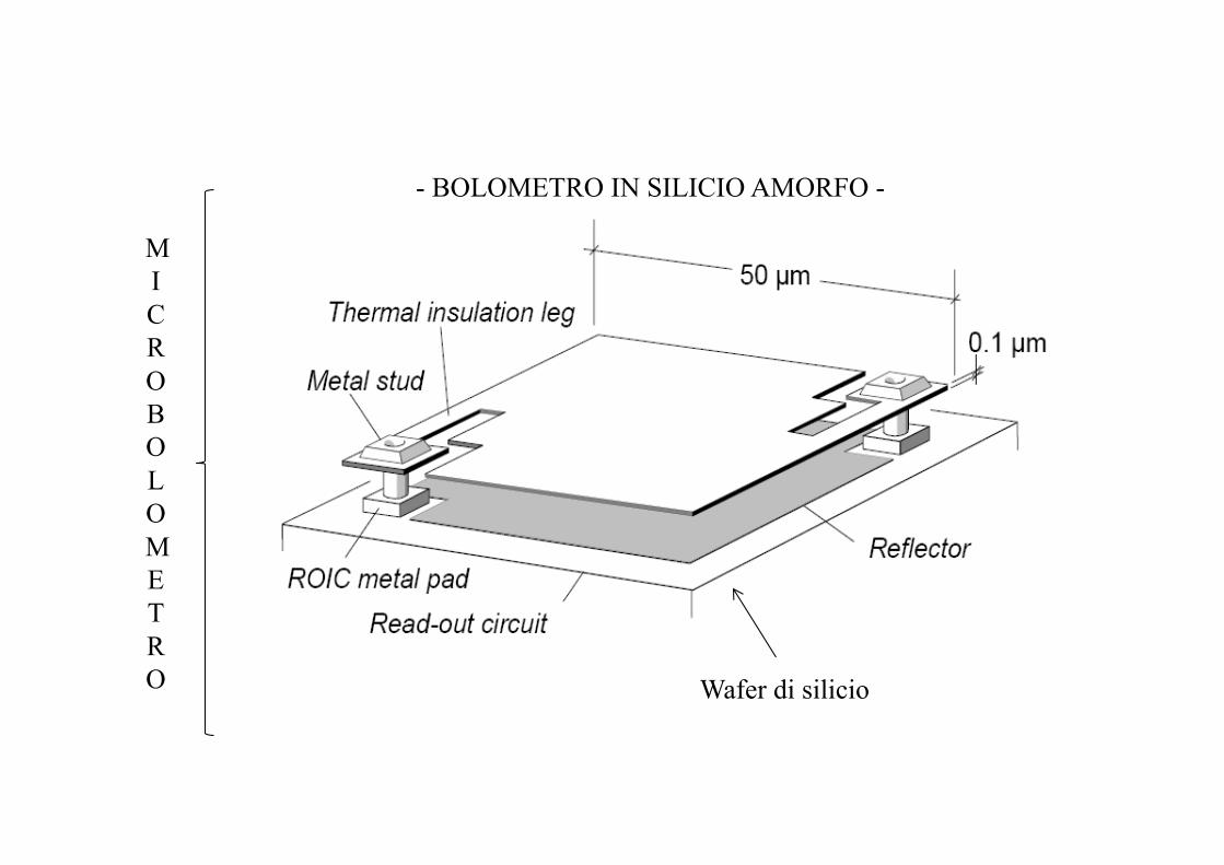
MICROBOLOMETRO Wafer di silicio
- BOLOMETRO IN SILICIO AMORFO -

Processo di fabbricazione direttamente su silicio
ROIC (readout integrated circuit)
Contatto elettricoStrato riflettente di alluminio
Deposizione del supporto di polymide
Incisione fino al ROICDeposizione film di
silicio amorfoDeposizione
elettrodo metallicoRimozione supporto di
polymide

Processo di fabbricazione direttamente su silicio

Esempi di chip microbolometrici
• Prima generazione: pacchetti metallici (dimensioni inferiori)
• Seconda generazione: pacchetti in ceramica (attualmente molto usati)
• Ultima generazione: pacchetti a wafer
ü Due wafer di Si usati per realizzare finestra ad infrarossiü Microbolometri chiusi sotto vuoto nelle cavità di silicioü Riduzione costi
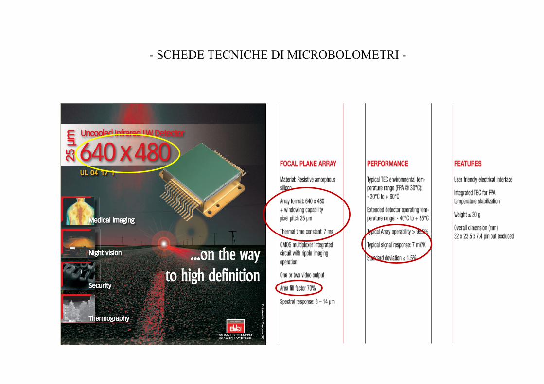
- SCHEDE TECNICHE DI MICROBOLOMETRI -
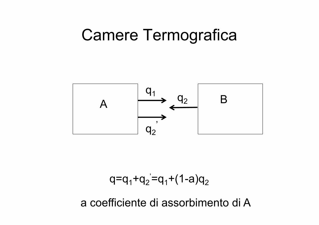
Camere Termografica
A Bq1
q2’
q2
q=q1+q2’=q1+(1-a)q2
a coefficiente di assorbimento di A

Camere Termografica
q=sT4
0
0.05
0.1
0.15
0 100 200 300 400 500
q (W
/m2 )
Temperature (k)
Andamento non lineare e quindi processo di calibrazione
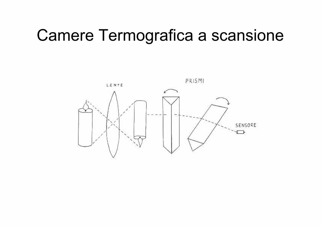
Camere Termografica a scansione

Camera a sensore singolo
Inside view of computerized thermal imaging system with mirrors that deflect infrared waves from a patient's breast to a camera below.
Focal plane array
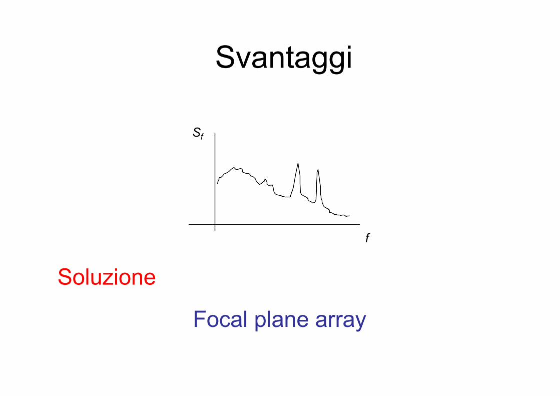
Svantaggi
!f
Sf
Soluzione
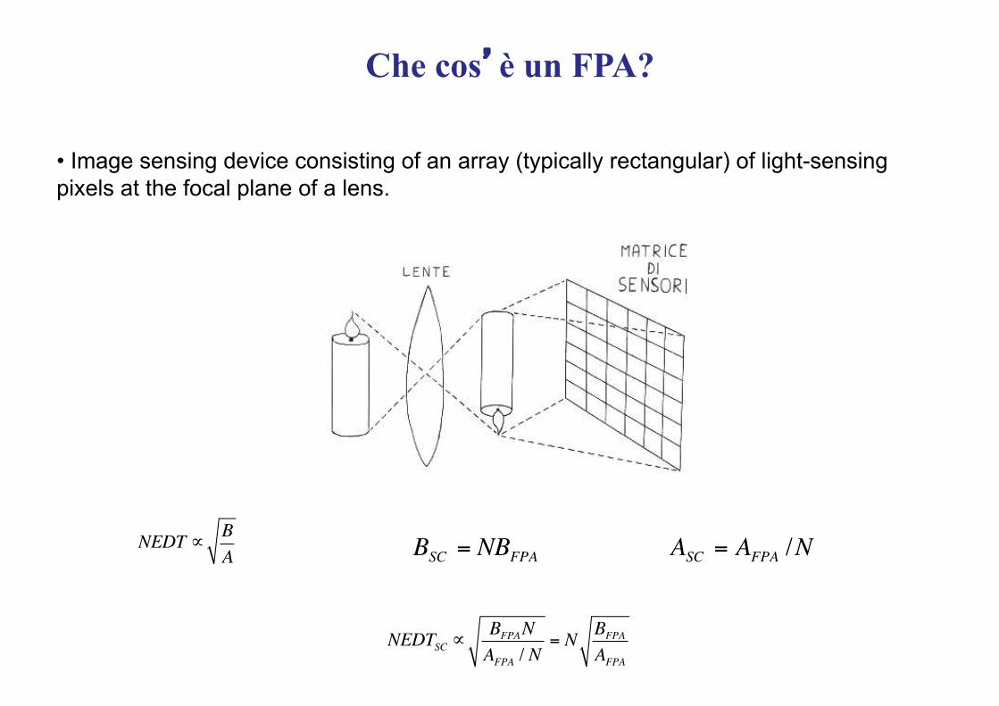
Che cos’è un FPA?
• Image sensing device consisting of an array (typically rectangular) of light-sensing pixels at the focal plane of a lens.
NEDT ∝ BA
NEDTSC ∝BFPANAFPA / N
= N BFPAAFPA€
BSC = NBFPA
€
ASC = AFPA /N

Detector Material Wavelength[μm] FPA Size Sensing Operability Cooling
InGaAs 0.9-1.6 320 x 240 Detection > 99% Uncooled
InSb 3.0 – 5.0 1024 x 1024 Detection > 99% Cooled 70K
QWIP (GaAs/AlGaAs) 8.0 – 9.0 512 x 512 Detection > 99% Cooled <70K
HgCdTe 1.0 – 20.0 1024x1024 Detection 85 - 95% Cooled 60-160K
Microbolometer 7.5-13.5 320 x 240 Absorption Typical of Uncooled Si process
Focal Plane Array Devices
Sensibilità termica fino a 30mk, velocità fino a 100frames/s, risoluzione fino a 25micron
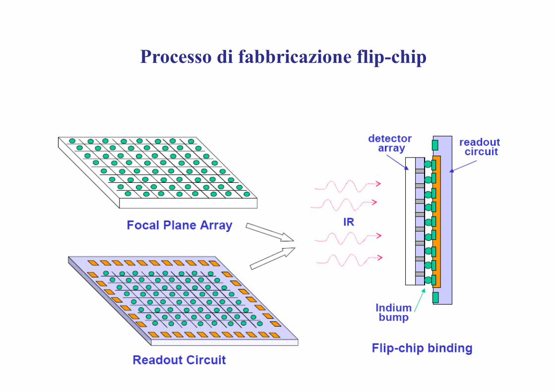
Processo di fabbricazione flip-chip
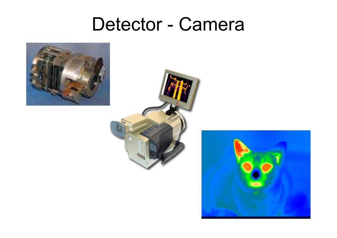
Detector - Camera

DetectorMHS 5000 SPECIFICATIONSCoolant: Thermoelectrically CooledDetector: MCT DetectorAutomatic Functions: Auto Focus, Auto AmbientWeight: 7.4 lbsSize: 221mm (w) x 147mm (H) x 270 mm (D)Operating Temperatures: 0-70 Degrees CelsiusImage Acquisition Temperature Range: 29 to 37 Degrees CelsiusThermal Sensitivity: <0.1 Degree CelsiusField Of View: 21.5 Horizontal And 21.5VerticalResolvable Elements: 255 (H) x 233 (V)Pixel Count: 57,000Image Capture Rate: 2 Scans Per SecondEmissivity Correction: 96%Image Storage: MHS/MHI/Bitmap FormatImage Display:5 x 16 True Color Palettes,1 x 16 Grayscale, 2 x 255 Inverted Grayscale,3 x 16 Step IsothermPower Options: AC Adaptor/Rechargeable Battery Pack

DetectorMHS 7000 SPECIFICATIONSDetector: MicrobolometerAutomatic Functions: Auto Focus, Auto AmbientWeight: 3.0 lbsSize: 3.7 (w) x 4.2 (H) x 6.5 (D)Operating Temperatures: 0-70 Degrees CelsiusImage Acquisition Temperature Range: 28 to 36 °CThermal Sensitivity: 0.08 Degree CelsiusField Of View: 29.0 Horizontal And 22.0 VerticalResolvable Elements: 320 (H) x 240 (V)Pixel Count: 76,800Image Capture Rate: 30 Frames/Second
60 Frames/Second (Selectable)Emissivity Correction: 98%Image Storage: MHS/MHI/Bitmap/MHVImage Display: 6 x 16 True Color Palettes,
2 x 256 True Color Palettes1 x 256 Grayscale,2 x 256 Inverted Grayscale3 x 16 Step Isotherm
Power Options: AC Adaptor
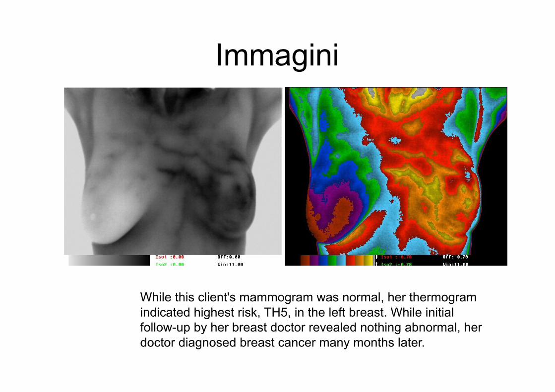
Immagini
While this client's mammogram was normal, her thermogram indicated highest risk, TH5, in the left breast. While initial follow-up by her breast doctor revealed nothing abnormal, her doctor diagnosed breast cancer many months later.

ImmaginiThis female’s complaint included pain. Thermal imaging revealed a previously undiagnosed right leg arteriovenous malformation over 27mm deep. As a result, the client was spared a sympathectomy. Vascular surgery corrected the problem.


![Rosanna Pinto – Ricercatore (rosanna.pinto@enea.it)mwl.diet.uniroma1.it/TeAB/Pinto_Valutazione esposizione RM_Roma 2017.pdf · Effetti biologici a RF e quadro normativo f [MHz]](https://static.fdocumenti.com/doc/165x107/5e2f05cee529514b0e118812/rosanna-pinto-a-ricercatore-eneaitmwldietuniroma1itteabpintovalutazione.jpg)


![00 Introduzione al corso 2015.ppt [modalità compatibilità]mwl.diet.uniroma1.it/TeAB/00_Introduzione_al_corso_2015.pdf · 2015-03-09 · • Anatomia e fisiologia dell’occhio ...](https://static.fdocumenti.com/doc/165x107/5f836b0759fdf070c73e12eb/00-introduzione-al-corso-2015ppt-modalit-compatibilitmwldiet-2015-03-09.jpg)