

Presentazione di PowerPoint - Intranet DEIBhome.deib.polimi.it/fiorini/Progettazione elettronica...
42
Laboratorio di Rivelatori di Radiazione e Strumentazione Nucleare Laboratorio di Rivelatori di Radiazione e Strumentazione Nucleare Argomenti per tesi: (per studenti sia BIO che ELN) • Rivelatori di immagini X e gamma per applicazioni nella diagnostica medicale, nell’astronomia X su satellite e nello studio delle materia • Circuiti integrati per l’elaborazione di segnali da rivelatori di radiazione per applicazioni scientifiche e industriali Requisiti: • conoscenze di base di elettronica • attitudine/interesse all’attività sperimentale di laboratorio • buona volontà Dipartimento di Elettronica e Informazione - Sezione di Elettronica
Transcript of Presentazione di PowerPoint - Intranet DEIBhome.deib.polimi.it/fiorini/Progettazione elettronica...
Laboratorio di Rivelatori di Radiazione
e Strumentazione Nucleare
Laboratorio di Rivelatori di Radiazionee Strumentazione Nucleare
Argomenti per tesi: (per studenti sia BIO che ELN)
• Rivelatori di immagini X e gamma per applicazioni nella
diagnostica medicale, nell’astronomia X su satellite e nello
studio delle materia
• Circuiti integrati per l’elaborazione di segnali da rivelatori
di radiazione per applicazioni scientifiche e industriali
Requisiti:
• conoscenze di base di elettronica
• attitudine/interesse all’attività sperimentale di laboratorio
• buona volontà
Dipartimento di Elettronica e Informazione - Sezione di Elettronica
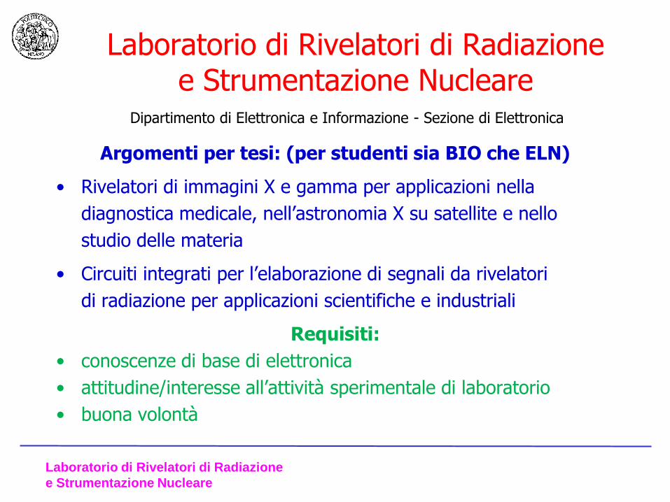
Application of the SDD in g-ray spectroscopy and imaging
Advantages of SDDs with respect to other photodetectors:
• high quantum efficiency (~ 90 %) @ 565nm of CsI(Tl)• compact, mechanical robust• no statistical spread due to multiplication• low operating voltages • smaller sensitivity to bias and temperature variations • insensitivity to magnetic fields
g-ray
scintillator
SDD
Applications:
• medical imaging• gamma-ray astronomy• homeland security• nuclear physics experiments

Anger Camera based on SDDs
collimator
continuous scintillator CsI(Tl)
monolithic array of photodetectors
photodetector counts
Main advantages (vs. pixellated detectors, e.g. CdTe or CZT):
• spatial resolution (<mm) achieved with ~ 10 times larger photodetector pixel size
1/100 readout channels needed for a given spatial resolution
• good detection efficiency, adjustable vs. energy with scintillator thickness
Main disadvantage
Poorer energy resolution, especially at low energy, due to the scintillator conversion
(although new scintillators like LaBr3 are reducing this gap) and to the electronics noise
added by the several photodetectors used for the light readout

The HICAM gamma camera
The consortium:
• Politecnico di Milano, Italy
• MPI Halbleiterlabor, Germany
• L’ACN, Italy
• Nuclear Fields Holland
• UCL London, UK
• OORR-Bg, Italy
• Hospital San Pau, Barcelona, Spain
• University of Milan, Italy
• Cf Consulting, Italy
features:
• 10x10cm2 FOV
• intrinsic resolution ~ 1mm
• overall resolution ~ 2.5mm @5cm
• energy resolution ~ 10% @140keV
• compactness
• compatibility with MRI
Applications:
• planar clinical studies of spine and small
bones
• intra-operative imaging of breast cancer
and melanoma
• imaging of parathyroid and thyroid
• SPECT measures in test phantoms
• combined HI-CAM and MRI measures
• small animal imaging
(EC contract n. LSHC-CT-2006-037737)
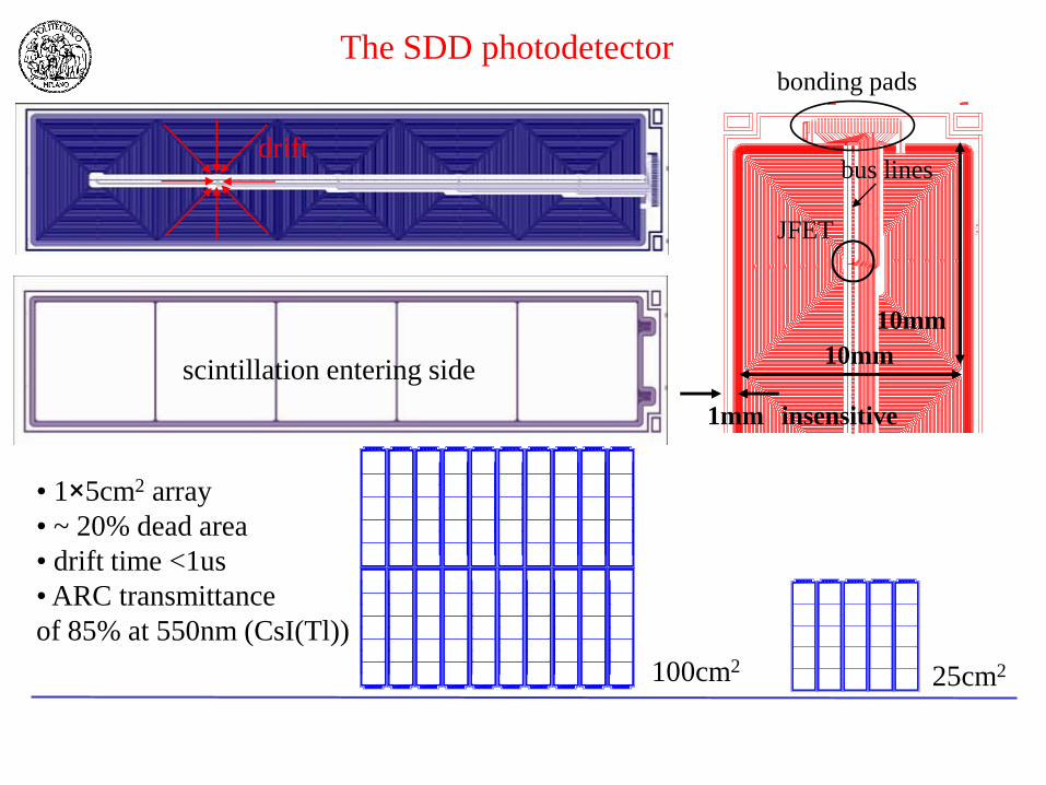
10mm
10mm
1mm insensitive
bonding pads
bus lines
JFET
The SDD photodetector
• 1×5cm2 array
• ~ 20% dead area
• drift time <1us
• ARC transmittance
of 85% at 550nm (CsI(Tl))
scintillation entering side
drift
100cm225cm2

The detection module
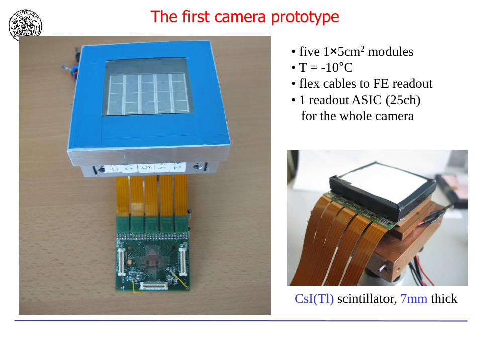
The first camera prototype
• five 1×5cm2 modules
• T = -10°C
• flex cables to FE readout
• 1 readout ASIC (25ch)
for the whole camera
CsI(Tl) scintillator, 7mm thick
Roberta Peloso
Politecnico di Milano & INFN
Roberta Peloso
Politecnico di Milano & INFNNSS-MIC 2010, Knoxville, 2 Nov. 2010
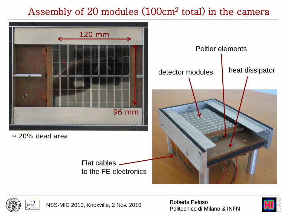
~ 20% dead area
Assembly of 20 modules (100cm2 total) in the camera
120 mm
96 mm
Flat cables
to the FE electronics
detector modules
Peltier elements
heat dissipator

Roberta Peloso
Politecnico di Milano & INFN
Roberta Peloso
Politecnico di Milano & INFNNSS-MIC 2010, Knoxville, 2 Nov. 2010
Biasing and readout electronics of the camera
25-channels readout circuit
0.35mm CMOS technology
flex from
detector module
25-channels
readout boards
(x4)
board including biasing
and interface with DAQ
(SPI programming and
data acquisition)

Roberta Peloso
Politecnico di Milano & INFN
Roberta Peloso
Politecnico di Milano & INFNNSS-MIC 2010, Knoxville, 2 Nov. 2010
Data Acquisition System
ADCs
LVD
S in
terfa
ce
ASICs managementFrame event generation
Ethernet frame serviceEthernet control service
Ethernet clientSimple user interfaceProcessing software
PC
Roberta Peloso
Politecnico di Milano & INFN
Roberta Peloso
Politecnico di Milano & INFNNSS-MIC 2010, Knoxville, 2 Nov. 2010
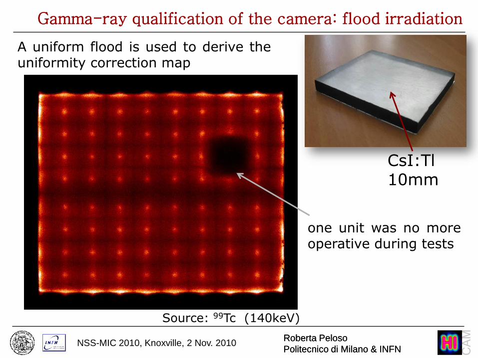
Gamma-ray qualification of the camera: flood irradiation
one unit was no moreoperative during tests
Source: 99Tc (140keV)
A uniform flood is used to derive theuniformity correction map
CsI:Tl10mm

Gamma-ray imaging: first results
99Tc source (140keV)
lead collimator
HICAM detector
Hole Ø=1mm
Pitch=3mm99Tc source placed at 90 cm
Roberta Peloso
Politecnico di Milano & INFN
Roberta Peloso
Politecnico di Milano & INFNNSS-MIC 2010, Knoxville, 2 Nov. 2010
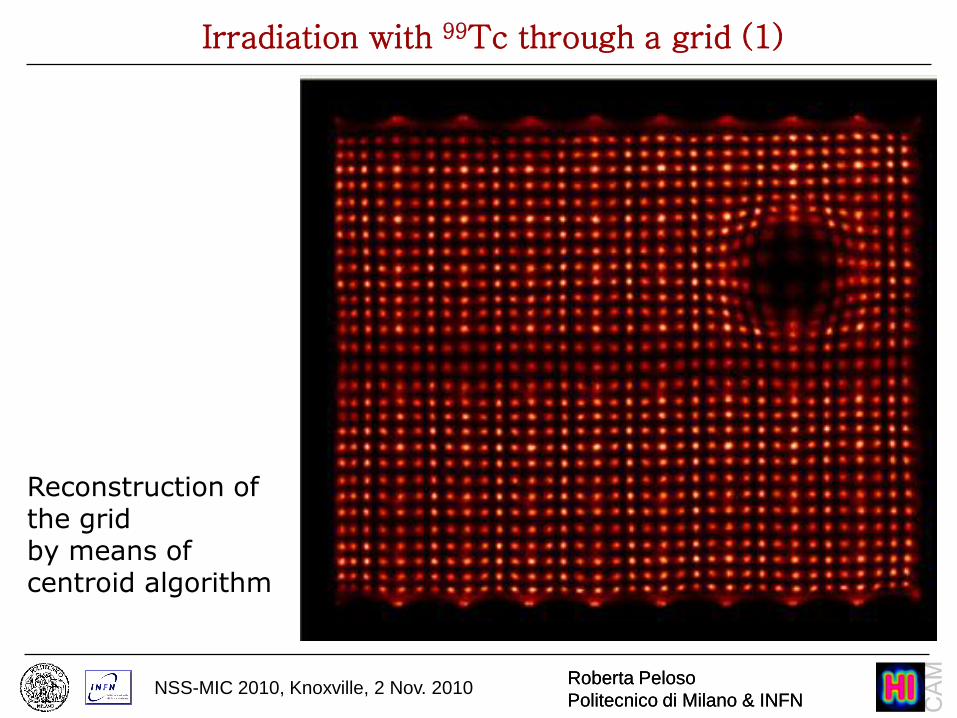
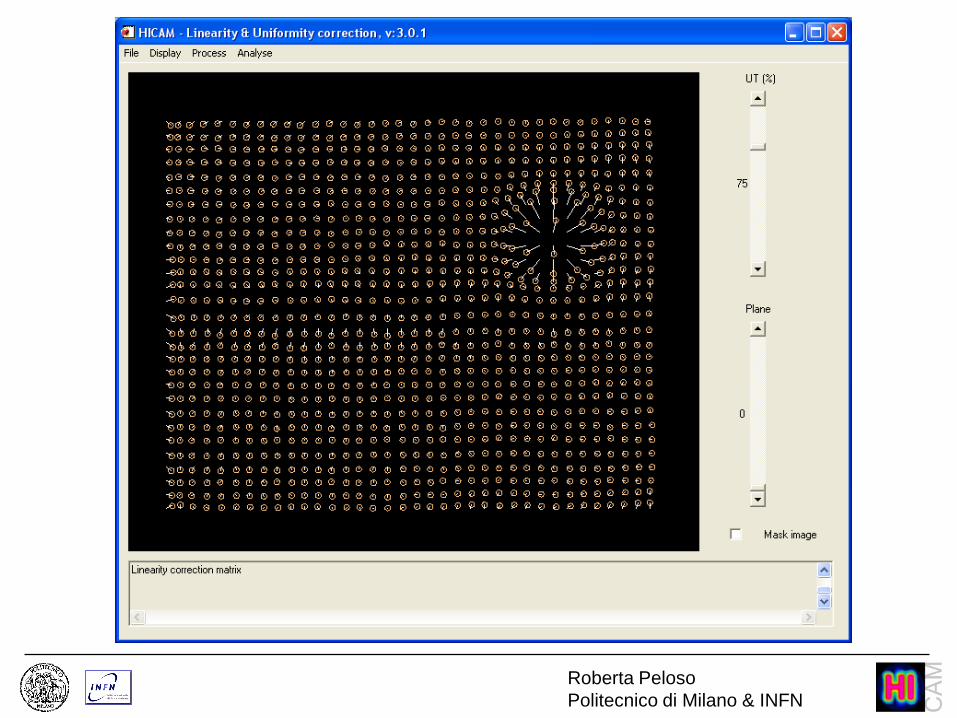
Irradiation with 99Tc through a grid (1)
Reconstruction ofthe gridby means ofcentroid algorithm
Roberta Peloso
Politecnico di Milano & INFN

Roberta Peloso
Politecnico di Milano & INFN
Roberta Peloso
Politecnico di Milano & INFNNSS-MIC 2010, Knoxville, 2 Nov. 2010
Mean FWHM =1.91mm
Mean FWHM =2.01mm
10,8 cm
8,7 cm
Irradiation with 99Tc through a grid (2)
X
Y
Roberta Peloso
Politecnico di Milano & INFN
Roberta Peloso
Politecnico di Milano & INFNNSS-MIC 2010, Knoxville, 2 Nov. 2010
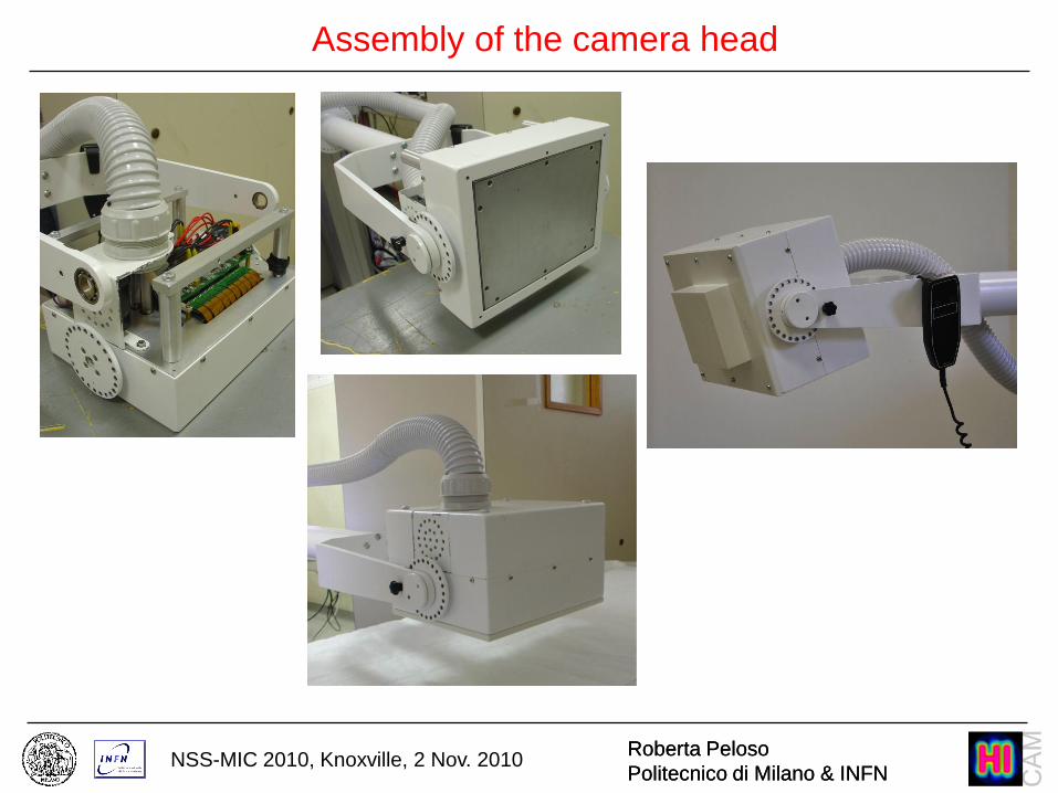
Assembly of the camera head
Roberta Peloso
Politecnico di Milano & INFN
Roberta Peloso
Politecnico di Milano & INFNNSS-MIC 2010, Knoxville, 2 Nov. 2010
Clinical trial: Thyroid acquisition
A)
B)
A)
B)
A)
B)
A)
B)
LEHRlenght =24 mmhole =1.11mmsepta thickness=0.16mm
A)
B)
A)
B)
A)
B)
A)
B)
hypo fixation at the left thyroid lobe
hyper fixation at the right thyroid lobe
HICAM
E-CAM
LEUHRlenght =45 mmhole =1.2mmsepta thickness 0.2mm
Roberta Peloso
Politecnico di Milano & INFN
Roberta Peloso
Politecnico di Milano & INFNNSS-MIC 2010, Knoxville, 2 Nov. 2010
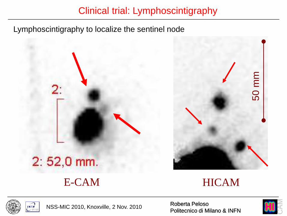
Clinical trial: Lymphoscintigraphy
50 m
m50 m
m
Lymphoscintigraphy to localize the sentinel node
HICAME-CAM

Roberta Peloso
Politecnico di Milano & INFN
Direct labelling
In vivo migration to LymphoNodes
of labelled and loaded DendriticCells
4
Imaging (MRI , Scint.)
mDC injection
Antigen Loading
2Labelling
with MNPs
mDC
3
111In-oxine
labelling Harvesting and
differentiation
1
iDC
Dendritic Cellpart of the immune system
Preclinical trials: cells imaging (1)

Roberta Peloso
Politecnico di Milano & INFN
Day 0 - 4 h
Tests carried out at Ospedale Sacco, Milano
DC+Ag+TNFa111In
Injection site
2 lymph nodes
Day 1 Day 2
kidneylymph node
Preclinical trials: cells imaging (2)
Shielded Injection site
Roberta Peloso
Politecnico di Milano & INFN
Roberta Peloso
Politecnico di Milano & INFNNSS-MIC 2010, Knoxville, 2 Nov. 2010
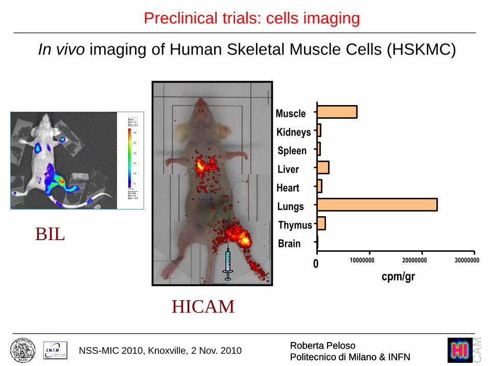
0 10000000 20000000 30000000
Brain
Thymus
Lungs
Heart
Liver
Spleen
Kidneys
Muscle
cpm/gr
In vivo imaging of Human Skeletal Muscle Cells (HSKMC)
Preclinical trials: cells imaging
HICAM
BIL

Perspective of gamma-ray imaging at medium-high energies (~MeV)
note: Compton interaction dominant
more than one interaction produces light in the scintillator
reconstruction has to retrieve multiple interactions from the
integral light distribution collected in the camera
possible solution: use Neural Networks reconstruction algorithm
05
1015
2025
3035
4045
50 0
5
10
15
20
25
30
35
40
45
50
0
500
1000
1500
2000
2500
Y
X
Photo
ns C
ount
first
interactionsecond
interaction
FWHM – Gaussian
FittingX Axis [mm] Y Axis [mm] Z Axis [mm] Energy [keV]
First Interaction Point 1.6 1.4 1.8 8.9
Second Interaction Point 2.6 2.9 3.5 -
FWHM – Gaussian
FittingX Axis [mm] Y Axis [mm] Z Axis [mm] Energy [keV]
First Interaction Point 1.6 1.4 1.8 8.9
Second Interaction Point 2.6 2.9 3.5 -
E=1MeV
Laboratorio di Rivelatori di Radiazione
e Strumentazione Nucleare
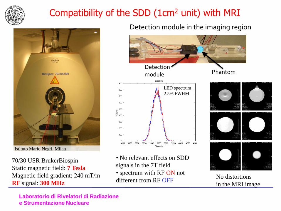
70/30 USR BrukerBiospin
Static magnetic field: 7 Tesla
Magnetic field gradient: 240 mT/m
RF signal: 300 MHz
Detection module in the imaging region
Detection module Phantom
No distortions
in the MRI image
• No relevant effects on SDD
signals in the 7T field
• spectrum with RF ON not
different from RF OFF
Compatibility of the SDD (1cm2 unit) with MRI
LED spectrum
2.5% FWHM
Istituto Mario Negri, Milan
Dresden, Germany, NSS 2008 [email protected]
Politecnico di Milano & INFN
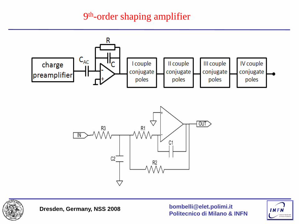
9th-order shaping amplifier

Dresden, Germany, NSS 2008 [email protected]
Politecnico di Milano & INFN
Semigaussian Parallel poles
simulations measurements
Tshaping ~ 140ns
Tpeaking ~ 470ns
Twidth 1% ~ 796ns
Tshaping ~ 176ns
Tpeaking ~ 600ns
Twidth 1% ~ 1016ns
Tshaping ~ 156ns
Tpeaking ~ 530ns
Twidth 1% ~ 760ns
Tshaping ~ 206ns
Tpeaking ~ 700ns
Twidth 1% ~ 1004ns

Laboratorio di Rivelatori di Radiazione
e Strumentazione Nucleare
The readout electronics and the DAQ system
40 channels
readout board
ASIC
front-end electronicsboards
USBconnectionto PC
ADCsboards
Dresden, Germany, NSS 2008 [email protected]
Politecnico di Milano & INFN
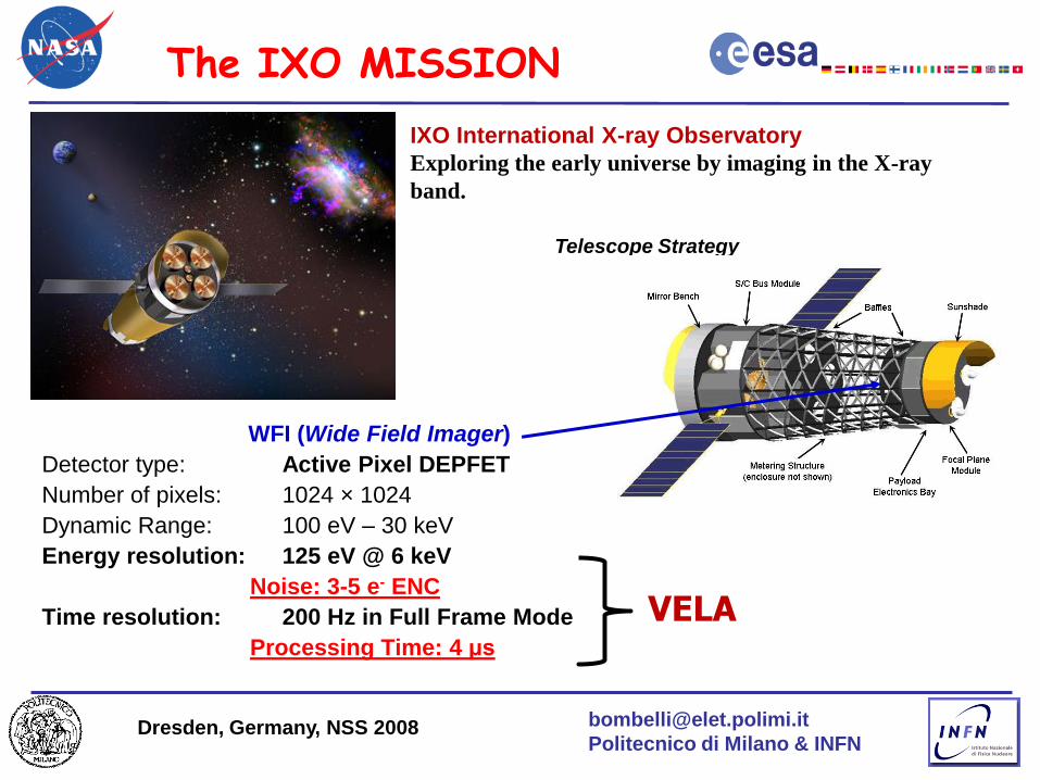
WFI (Wide Field Imager)
Detector type: Active Pixel DEPFET
Number of pixels: 1024 × 1024
Dynamic Range: 100 eV – 30 keV
Energy resolution: 125 eV @ 6 keV
Noise: 3-5 e- ENC
Time resolution: 200 Hz in Full Frame Mode
Processing Time: 4 μs
The IXO MISSION
IXO International X-ray Observatory
Exploring the early universe by imaging in the X-ray
band.
Telescope Strategy
VELA
Laboratorio di Rivelatori di Radiazione
e Strumentazione Nucleare
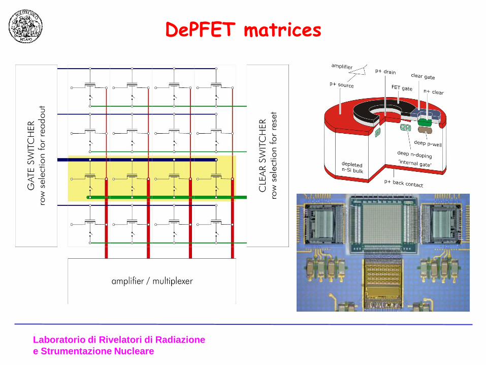
DePFET matrices
Dresden, Germany, NSS 2008 [email protected]
Politecnico di Milano & INFN
The VELA Current Readout Scheme
Gq = 200 pA/el
Trapezoidal
Shaper
Virtual Ground
Current Source
Current Step
No change in DEPFET voltages during the readout.
The gain in not limited by the DEPFET output resistance
Fast readout
High bias current to
achieve best resolution

Dresden, Germany, NSS 2008 [email protected]
Politecnico di Milano & INFN
VELA ASIC layout
0.35 µm AMS CMOS, 3.3V
Chip size is 5.2 mm x 4.6 mm

Milano, 22 Luglio 2008 X-Ray Free Electron Laser 33
“XFEL”= X-Free Electron Laser (@Hamburg-Bahrenfeld)
proprietà ottiche dei laser convenzionali
+differenti principi di funzionamento:
Il progetto XFEL
Macro-bunching&SASE(Self-Amplified-Spontaneous-Emission)
Dresden, Germany, NSS 2008 [email protected]
Politecnico di Milano & INFNMilano, 22 Ottobre 2009 34
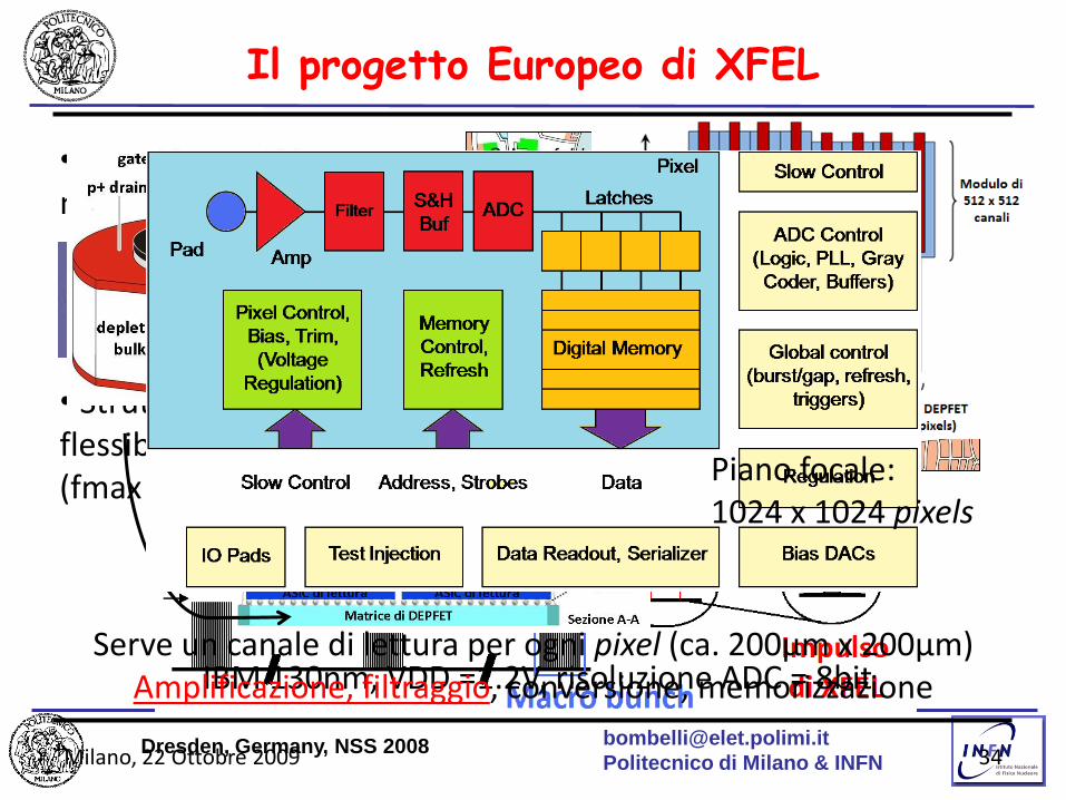
Il progetto Europeo di XFEL
• In costruzionenell’area di Amburgo
• Struttura temporaleflessibile degli impulsi(fmax = 5MHz)
IBM 130nm, VDD =1.2V, risoluzione ADC = 8bitServe un canale di lettura per ogni pixel (ca. 200μm x 200μm)
Amplificazione, filtraggio, conversione, memorizzazione
Piano focale:1024 x 1024 pixels
Leicester, 1 October 2010 [email protected]
Politecnico di Milano & INFN
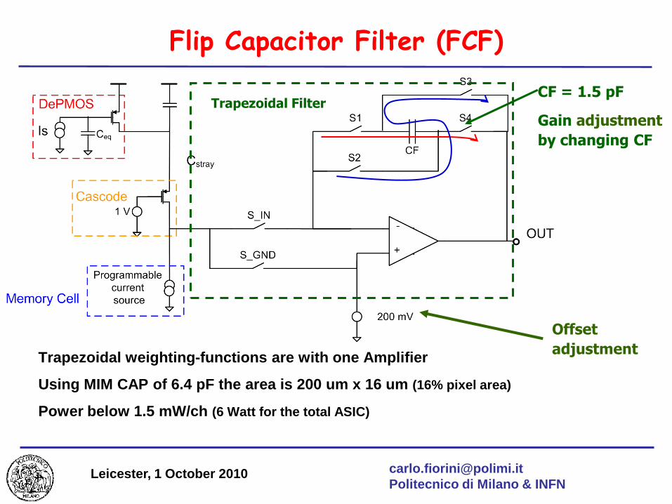
Flip Capacitor Filter (FCF)
Trapezoidal weighting-functions are with one Amplifier
Using MIM CAP of 6.4 pF the area is 200 um x 16 um (16% pixel area)
Power below 1.5 mW/ch (6 Watt for the total ASIC)
Trapezoidal FilterCF = 1.5 pF
Gain adjustment
by changing CF
Offset
adjustment
Dresden, Germany, NSS 2008 [email protected]
Politecnico di Milano & INFNMilano, 22 Ottobre 2009 36
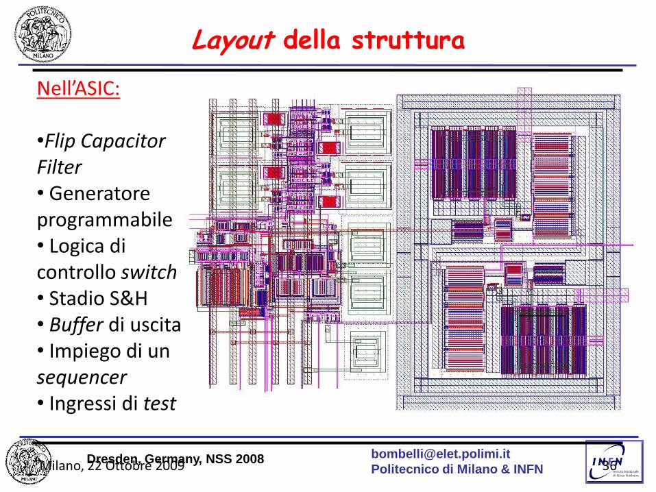
Layout della struttura
Nell’ASIC:
•Flip CapacitorFilter• Generatoreprogrammabile• Logica di controllo switch• Stadio S&H• Buffer di uscita• Impiego di unsequencer• Ingressi di test
Leicester, 1 October 2010 [email protected]
Politecnico di Milano & INFN
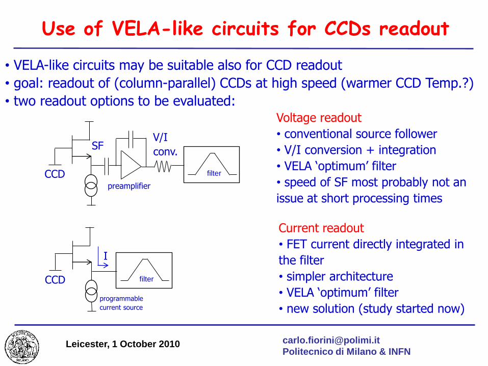
Use of VELA-like circuits for CCDs readout
Voltage readout
• conventional source follower
• V/I conversion + integration
• VELA ‘optimum’ filter
• speed of SF most probably not an
issue at short processing times
• VELA-like circuits may be suitable also for CCD readout
• goal: readout of (column-parallel) CCDs at high speed (warmer CCD Temp.?)
• two readout options to be evaluated:
filterCCD
SF
preamplifier
V/I
conv.
filterCCD
programmable
current source
I
Current readout
• FET current directly integrated in
the filter
• simpler architecture
• VELA ‘optimum’ filter
• new solution (study started now)

Progettazione di circuiti integrati: schematico e simulazioni
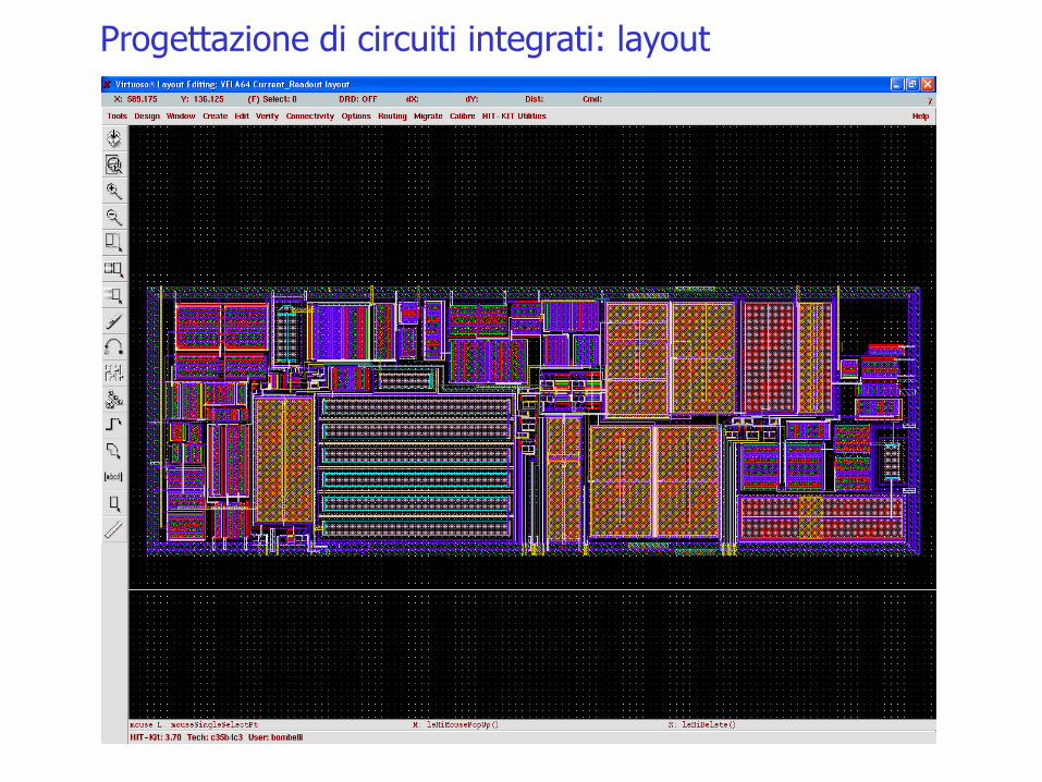
Progettazione di circuiti integrati: layout
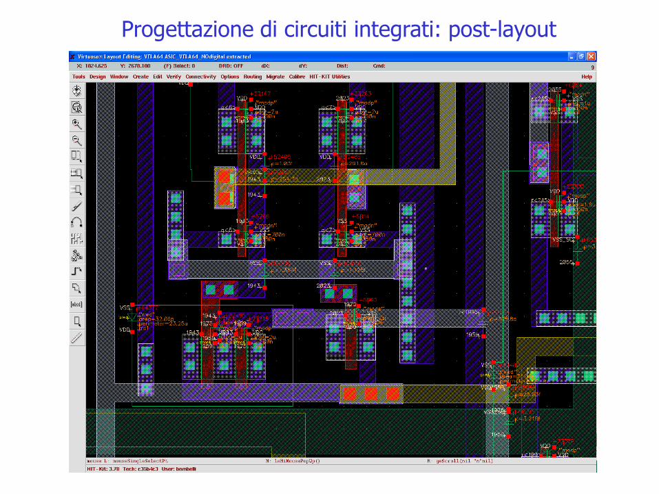
Progettazione di circuiti integrati: post-layout

Sviluppo del set-up sperimentale e test

Dresden, Germany, NSS 2008 [email protected]
Politecnico di Milano & INFN
Lista tesi disponibili
• La gamma camera HICAM: ottimizzazione e applicazioni
• Imager per gamma ad alta energia (reti neurali)
• Circuito VELA per la lettura di CCD
• Circuito integrato per SDD per IXO e per un esperimento
di fisica nucleare (Siddharta) ai laboratori INFN di Frascati
• Circuito per la lettura di pixels nel progetto XFEL
• Diversi circuiti per spettroscopia X e per sistemi di
monitoraggio delle radiazioni (imp. nucleare, sicurezza,
identificazione di sorgenti radioattive nei rottami metallici
utilizzati nelle acciaierie, ecc.)*
*tesi nell’ambitodicollaborazioniconindustrie