Low temperature growth of fully covered single-layer ...
9
Nanoscale PAPER Cite this: Nanoscale, 2017, 9, 14467 Received 10th April 2017, Accepted 27th August 2017 DOI: 10.1039/c7nr02553j rsc.li/nanoscale Low temperature growth of fully covered single-layer graphene using a CoCu catalyst† Hisashi Sugime, * a,b Lorenzo D’Arsié, b Santiago Esconjauregui, b Guofang Zhong, b Xingyi Wu, b Eugen Hildebrandt, b Hikmet Sezen, c Matteo Amati, c Luca Gregoratti, c Robert S. Weatherup b and John Robertson b A bimetallic CoCu alloy thin-film catalyst is developed that enables the growth of uniform, high-quality graphene at 750 °C in 3 min by chemical vapour deposition. The growth outcome is found to vary signifi- cantly as the Cu concentration is varied, with ∼1 at% Cu added to Co yielding complete coverage single- layer graphene growth for the conditions used. The suppression of multilayer formation is attributable to Cu decoration of high reactivity sites on the Co surface which otherwise serve as preferential nucleation sites for multilayer graphene. X-ray photoemission spectroscopy shows that Co and Cu form an alloy at high temperatures, which has a drastically lower carbon solubility, as determined by using the calculated Co–Cu–C ternary phase diagram. Raman spectroscopy confirms the high quality (I D /I G < 0.05) and spatial uniformity of the single-layer graphene. The rational design of a bimetallic catalyst highlights the potential of catalyst alloying for producing two-dimensional materials with tailored properties. Introduction Graphene’s 2D structure, excellent electronic properties, and chemical stability 1–4 make it a promising material for device applications including transparent electrodes, sensors, and passivating layers. 5–7 Chemical vapour deposition (CVD) has emerged as the most scalable and versatile technique to grow graphene for such applications, where a high-quality material is typically required. 8,9 Uniform single-layer graphene (SLG) has been well demonstrated on low-cost polycrystalline Cu foils over a broad window of processing conditions, 10–13 leading to the widespread adoption of Cu-based catalysts, with full coverage SLG consisting of millimetre-scale domains achievable through appropriate catalyst treatments. 14 To obtain large domain sizes and low defect densities, growth is typically performed at relatively high growth temperatures (>1000 °C) on thick catalyst foils (∼25 μm). 15 These conditions are not readily compatible with many established device materials or thin-film patterning/processing methods, limiting the potential for direct integration. Current approaches to device fabrication from CVD graphene therefore rely for the most part on transfer to a target substrate, which is far from straightforward, with many opportunities for deleterious con- tamination and mechanical damage to be introduced. 16 Furthermore, given that significant Cu sublimation leads to roughening of the catalyst surface at the growth temperature, 17 there is inevitable wrinkling of the material when it is trans- ferred to the target substrate. For direct integration, methods are therefore needed to grow high-quality SLG on selected thin-film materials at low temperatures, allowing facile incor- poration into device structures, 18,19 as well as increased scal- ability and reduced production costs. This requires the rational design of the catalyst support and growth process to achieve a desired outcome, which is only possible through a detailed understanding of the underlying growth mechanisms and how they can be controlled. At lower temperatures, Ni, Co, and Fe show higher catalytic activities than Cu, both for hydrocarbon dissociation and carbon incorporation into graphitic structures. Indeed, they have been widely employed as catalysts for the low temperature growth of carbon nanotubes. 20–27 However, attempts to grow polycrystalline thin-films of these metals have generally resulted in the formation of inhomogeneous multi-layer graphene. 28–33 This has often been attributed to the high carbon solubility of these metals, based on the assumption that carbon dissolved in the catalyst precipitates as multilayer graphene on cooling. 11,34 However, extensive in situ studies confirm that growth, including multilayer formation, occurs predominantly isothermally at typical growth temperatures. 35–44 This multilayer formation is related to high catalytic activity of † Electronic supplementary information (ESI) available. See DOI: 10.1039/ C7NR02553J a Waseda Institute for Advanced Study, Waseda University, Tokyo 169-8050, Japan. E-mail: [email protected]; Tel: +81-3-5286-2769 b Department of Engineering, University of Cambridge, Cambridge CB3 0FA, UK c Elettra-Sincrotrone Trieste S.C.p.A., AREA Science Park, S.S. 14 km 163.5, 34149 Trieste, Italy This journal is © The Royal Society of Chemistry 2017 Nanoscale, 2017, 9, 14467–14475 | 14467 Open Access Article. Published on 28 August 2017. Downloaded on 2/24/2022 7:02:51 AM. This article is licensed under a Creative Commons Attribution 3.0 Unported Licence. View Article Online View Journal | View Issue
Transcript of Low temperature growth of fully covered single-layer ...
Nanoscale
PAPER
Cite this: Nanoscale, 2017, 9, 14467
Received 10th April 2017,Accepted 27th August 2017
DOI: 10.1039/c7nr02553j
rsc.li/nanoscale
Low temperature growth of fully coveredsingle-layer graphene using a CoCu catalyst†
Hisashi Sugime, *a,b Lorenzo D’Arsié, b Santiago Esconjauregui, b
Guofang Zhong, b Xingyi Wu, b Eugen Hildebrandt,b Hikmet Sezen, c
Matteo Amati,c Luca Gregoratti,c Robert S. Weatherup b and John Robertsonb
A bimetallic CoCu alloy thin-film catalyst is developed that enables the growth of uniform, high-quality
graphene at 750 °C in 3 min by chemical vapour deposition. The growth outcome is found to vary signifi-
cantly as the Cu concentration is varied, with ∼1 at% Cu added to Co yielding complete coverage single-
layer graphene growth for the conditions used. The suppression of multilayer formation is attributable to
Cu decoration of high reactivity sites on the Co surface which otherwise serve as preferential nucleation
sites for multilayer graphene. X-ray photoemission spectroscopy shows that Co and Cu form an alloy at
high temperatures, which has a drastically lower carbon solubility, as determined by using the calculated
Co–Cu–C ternary phase diagram. Raman spectroscopy confirms the high quality (ID/IG < 0.05) and spatial
uniformity of the single-layer graphene. The rational design of a bimetallic catalyst highlights the potential
of catalyst alloying for producing two-dimensional materials with tailored properties.
Introduction
Graphene’s 2D structure, excellent electronic properties, andchemical stability1–4 make it a promising material for deviceapplications including transparent electrodes, sensors, andpassivating layers.5–7 Chemical vapour deposition (CVD) hasemerged as the most scalable and versatile technique to growgraphene for such applications, where a high-quality materialis typically required.8,9 Uniform single-layer graphene (SLG)has been well demonstrated on low-cost polycrystalline Cufoils over a broad window of processing conditions,10–13
leading to the widespread adoption of Cu-based catalysts, withfull coverage SLG consisting of millimetre-scale domainsachievable through appropriate catalyst treatments.14 Toobtain large domain sizes and low defect densities, growth istypically performed at relatively high growth temperatures(>1000 °C) on thick catalyst foils (∼25 µm).15 These conditionsare not readily compatible with many established devicematerials or thin-film patterning/processing methods, limitingthe potential for direct integration. Current approaches todevice fabrication from CVD graphene therefore rely for the
most part on transfer to a target substrate, which is far fromstraightforward, with many opportunities for deleterious con-tamination and mechanical damage to be introduced.16
Furthermore, given that significant Cu sublimation leads toroughening of the catalyst surface at the growth temperature,17
there is inevitable wrinkling of the material when it is trans-ferred to the target substrate. For direct integration, methodsare therefore needed to grow high-quality SLG on selectedthin-film materials at low temperatures, allowing facile incor-poration into device structures,18,19 as well as increased scal-ability and reduced production costs. This requires the rationaldesign of the catalyst support and growth process to achieve adesired outcome, which is only possible through a detailedunderstanding of the underlying growth mechanisms and howthey can be controlled.
At lower temperatures, Ni, Co, and Fe show higher catalyticactivities than Cu, both for hydrocarbon dissociation andcarbon incorporation into graphitic structures. Indeed, theyhave been widely employed as catalysts for the low temperaturegrowth of carbon nanotubes.20–27 However, attempts to growpolycrystalline thin-films of these metals have generallyresulted in the formation of inhomogeneous multi-layergraphene.28–33 This has often been attributed to the highcarbon solubility of these metals, based on the assumptionthat carbon dissolved in the catalyst precipitates as multilayergraphene on cooling.11,34 However, extensive in situ studiesconfirm that growth, including multilayer formation, occurspredominantly isothermally at typical growth temperatures.35–44
This multilayer formation is related to high catalytic activity of†Electronic supplementary information (ESI) available. See DOI: 10.1039/C7NR02553J
aWaseda Institute for Advanced Study, Waseda University, Tokyo 169-8050, Japan.
E-mail: [email protected]; Tel: +81-3-5286-2769bDepartment of Engineering, University of Cambridge, Cambridge CB3 0FA, UKcElettra-Sincrotrone Trieste S.C.p.A., AREA Science Park, S.S. 14 km 163.5,
34149 Trieste, Italy
This journal is © The Royal Society of Chemistry 2017 Nanoscale, 2017, 9, 14467–14475 | 14467
Ope
n A
cces
s A
rtic
le. P
ublis
hed
on 2
8 A
ugus
t 201
7. D
ownl
oade
d on
2/2
4/20
22 7
:02:
51 A
M.
Thi
s ar
ticle
is li
cens
ed u
nder
a C
reat
ive
Com
mon
s A
ttrib
utio
n 3.
0 U
npor
ted
Lic
ence
.
View Article OnlineView Journal | View Issue
these catalysts which can result in direct multilayer nucleation,or the thin-film catalysts becoming rapidly saturated withcarbon throughout their thickness with additional carbon dis-sociation feeding multilayer formation.45,46 This can beavoided by using thick catalyst foils, where the supply ofcarbon from the gas-phase is mediated by ongoing carbondiffusion into the catalyst bulk, resulting in a broad processingwindow over which uniform SLG can be stabilised.45,46
Alternatively single-crystalline substrates may be used, wherecareful control of the exposure conditions can yield epitaxial,SLG on specific surface orientations.38,40,43,47,48 Howeverneither of these approaches can be readily integrated withstandard lithographic processing steps used in fabricatingdevice structures.
Catalyst alloying provides a means of tuning surface reactiv-ity that can be directly applied to thin-film catalyst materials.For example, by decorating high-reactivity sites on polycrystal-line Ni with Au we have previously demonstrated the suppres-sion of multilayer growth, with uniform SLG formed at temp-eratures as low as 450 °C.37,41,45,49 On the other hand, widen-ing the selection of ferromagnetic materials on which SLG canbe formed is of significant importance for applications.For example, SLG-covered Co electrodes show enhanced per-pendicular magnetic anisotropy,50 remain stable against oxi-dation in air,7,51 and are promising as spin filtering electro-des.52 However, the low temperature growth of SLG with thinCo catalysts has not been reported. In this paper, we considerthe addition of less catalytically active Cu to the surface of Cothin-films, to tune the graphene growth behaviour. Using anoriginal combinatorial method,53,54 we investigate the effect ofthe alloy ratio on the growth of graphene, and find that thereis an optimum thickness for Cu to maximize the coverage ofSLG. With the optimum condition, we demonstrate the for-mation of full coverage, high quality SLG on sputtered CoCucatalyst films with a simple thermal CVD process at relativelylow temperatures. The underlying mechanisms that leadto this improvement are systematically investigated usingex situ growth calibrations, in situ scanning photoemissionmicroscopy (SPEM), and calculated ternary phase diagrams.The Cu is found to decorate high reactivity sites on theCo surface, suppressing multilayer graphene nucleation andresulting in exclusively SLG formation. We thereby demon-strate that the approach of catalyst alloying can be extended totune graphene growth on different transition metal catalysts,offering new opportunities for directly integrating grapheneinto device structures.
Results
We first investigate the effect of the catalyst composition onthe graphene growth using combinatorial CoCu samples.Fig. 1a shows a schematic of the combinatorial method.53,54
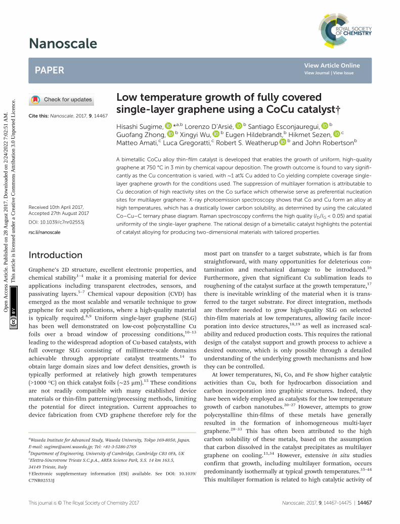
We make a thickness gradient of Cu (∼0.3–20 nm) on uniformCo (500 nm) in one direction (∼10 mm in length) by using aslit mask. The area with the thickest Cu (∼20 nm) appears
slightly orange in colour before graphene growth (left area inFig. 1b). Fig. 1c shows SEM images of graphene grown on theCoCu catalyst at 750 °C for 3 min, and OM images followingtransfer of the graphene to SiO2 (300 nm)/Si. The Cu thicknessrange considered in Fig. 1c corresponds to the area shownwith the dashed rectangle in the Fig. 1b. Depending on the Cuthickness, the graphene grows with different nucleation den-sities, numbers of layers, and grain sizes. Multilayer graphenegrows when the Cu adlayer is less than ∼2.4 nm thick (rightpart of Fig. 1c). We note that the contrast associated with multi-layer graphene is most apparent in the OM images followingtransfer of the graphene onto SiO2(300 nm)/Si.55,56 Increasingthe Cu thickness to ∼3.8 nm results in a SLG coverage of∼90%, whilst with ∼6.0 nm of Cu full SLG coverage is achievedas highlighted with the red rectangle in Fig. 1c. Furtherincreasing the Cu thickness results in the formation of bilayerand multilayer graphene regions as readily apparent with∼10 nm of Cu (leftmost images in Fig. 1c).
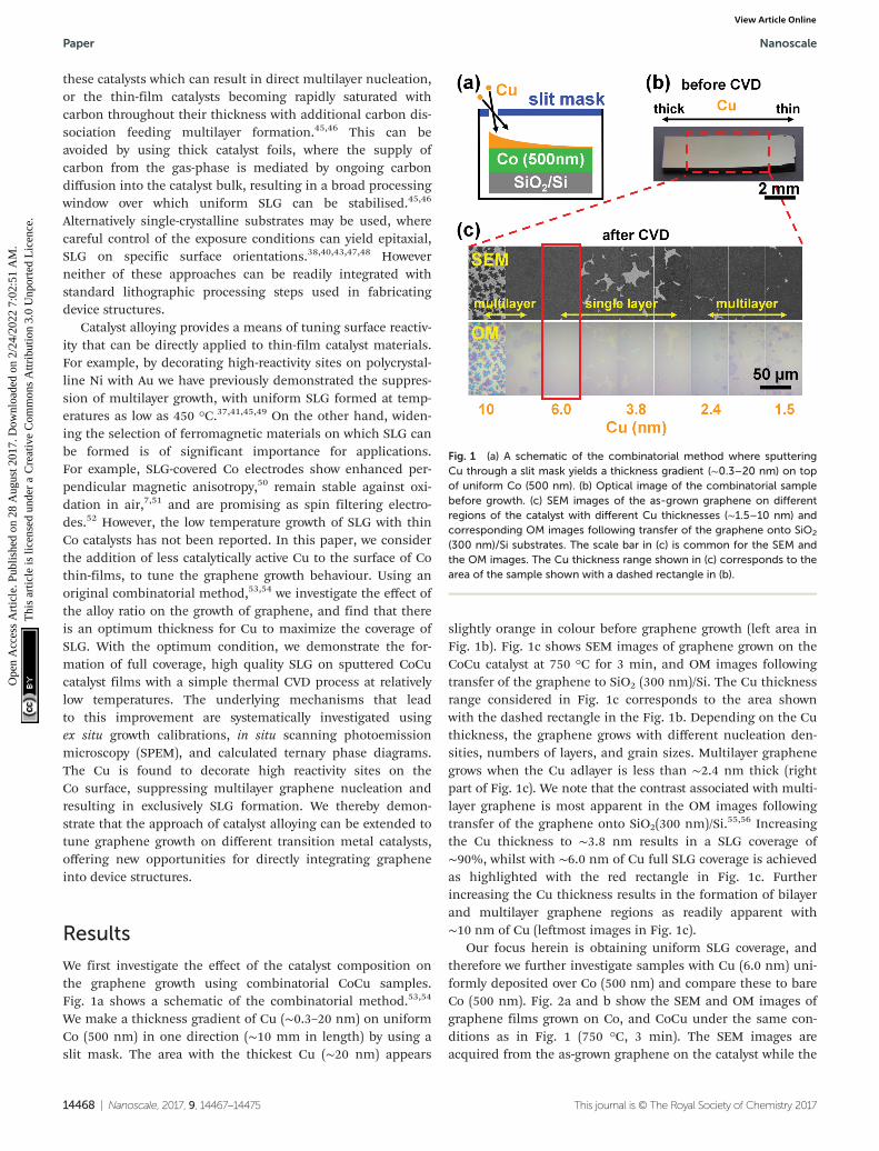
Our focus herein is obtaining uniform SLG coverage, andtherefore we further investigate samples with Cu (6.0 nm) uni-formly deposited over Co (500 nm) and compare these to bareCo (500 nm). Fig. 2a and b show the SEM and OM images ofgraphene films grown on Co, and CoCu under the same con-ditions as in Fig. 1 (750 °C, 3 min). The SEM images areacquired from the as-grown graphene on the catalyst while the
Fig. 1 (a) A schematic of the combinatorial method where sputteringCu through a slit mask yields a thickness gradient (∼0.3–20 nm) on topof uniform Co (500 nm). (b) Optical image of the combinatorial samplebefore growth. (c) SEM images of the as-grown graphene on differentregions of the catalyst with different Cu thicknesses (∼1.5–10 nm) andcorresponding OM images following transfer of the graphene onto SiO2
(300 nm)/Si substrates. The scale bar in (c) is common for the SEM andthe OM images. The Cu thickness range shown in (c) corresponds to thearea of the sample shown with a dashed rectangle in (b).
Paper Nanoscale
14468 | Nanoscale, 2017, 9, 14467–14475 This journal is © The Royal Society of Chemistry 2017
Ope
n A
cces
s A
rtic
le. P
ublis
hed
on 2
8 A
ugus
t 201
7. D
ownl
oade
d on
2/2
4/20
22 7
:02:
51 A
M.
Thi
s ar
ticle
is li
cens
ed u
nder
a C
reat
ive
Com
mon
s A
ttrib
utio
n 3.
0 U
npor
ted
Lic
ence
.View Article Online
OM images are taken after transferring the graphene toSiO2(300 nm)/Si substrates. As observed with the combinator-ial samples in Fig. 1, the sample with elemental Co yields com-plete coverage with inhomogeneous multilayer graphene,while the CoCu sample is completely covered with uniformSLG. We note that if the Ti adhesion layer is not present underthe Co film, it is found to dewet at high temperature and formholes of ∼300 nm diameter (see Fig. S1†).
Fig. 2c shows the Raman spectra of the samples in Fig. 2aand b. With the elemental Co sample, we observe the D-peakat 1348 cm−1, the G-peak at 1582 cm−1 with full width at halfmaximum (FWHM) of 36 cm−1, and the 2D-peak at 2697 cm−1
(FWHM: 96 cm−1). The ID/IG ratio is 0.18 and the I2D/IG ratio is0.61, which along with the large FWHM of the 2D-peak areconsistent with those reported for reasonably defective multi-layer graphene. With the CoCu sample, on the other hand, weobserve a very small D-peak at 1359 cm−1, the G-peak at1593 cm−1 (FWHM: 16 cm−1), and the 2D-peak at 2683 cm−1
(FWHM: 35 cm−1). The small ID/IG ratio of under 0.05, I2D/IGratio of 2.1, and narrow 2D-peak which is well-fitted by asingle-lorentzian confirm the presence of high quality SLG.57
We note that there is an increase in the ID/IG ratio to 0.38 asthe growth temperature is lowered to 700 °C (50 °C lower thanthe standard condition) indicating deterioration in the gra-
phene crystallinity (see Fig. S2†). For the CoCu samplegrown under standard conditions, we perform Ramanmapping over a 40 × 40 µm2 area with a pitch of 2 µm. Fig. 2d,e, and f show maps of the I2D/IG ratio, ID/IG ratio, and 2DFWHM, respectively. In the mapped area, it is confirmed that95% has a I2D/IG ratio >1.8, 93% has a ID/IG ratio <0.10, and94% has a FWHM <39 cm−1 which confirms the good spatialuniformity of the SLG. In addition to Raman spectroscopywhich gives a relatively direct measure of defect density basedon the ID/IG ratio,58 we have also measured the carrier mobilityof the graphene which provides a more indirect indicator ofgraphene quality. Hall effect measurements on a device madefrom the graphene on SiO2(300 nm)/Si reveal that the holemobility is ∼1100 cm2 V−1 s−1 for a carrier concentration of∼3.9 × 1012 cm−2 under ambient conditions. The carrier con-centration herein shows a slightly higher value than that ofgraphene grown on elemental Cu catalysts in our previousstudy (∼1.5 × 1012 cm−2) with the same measurement setup.59
However we note that this falls within the variation expectedas a result of the transfer process and processing in air, wherepolymer and etchant residues and air-borne contaminants canalter the doping.
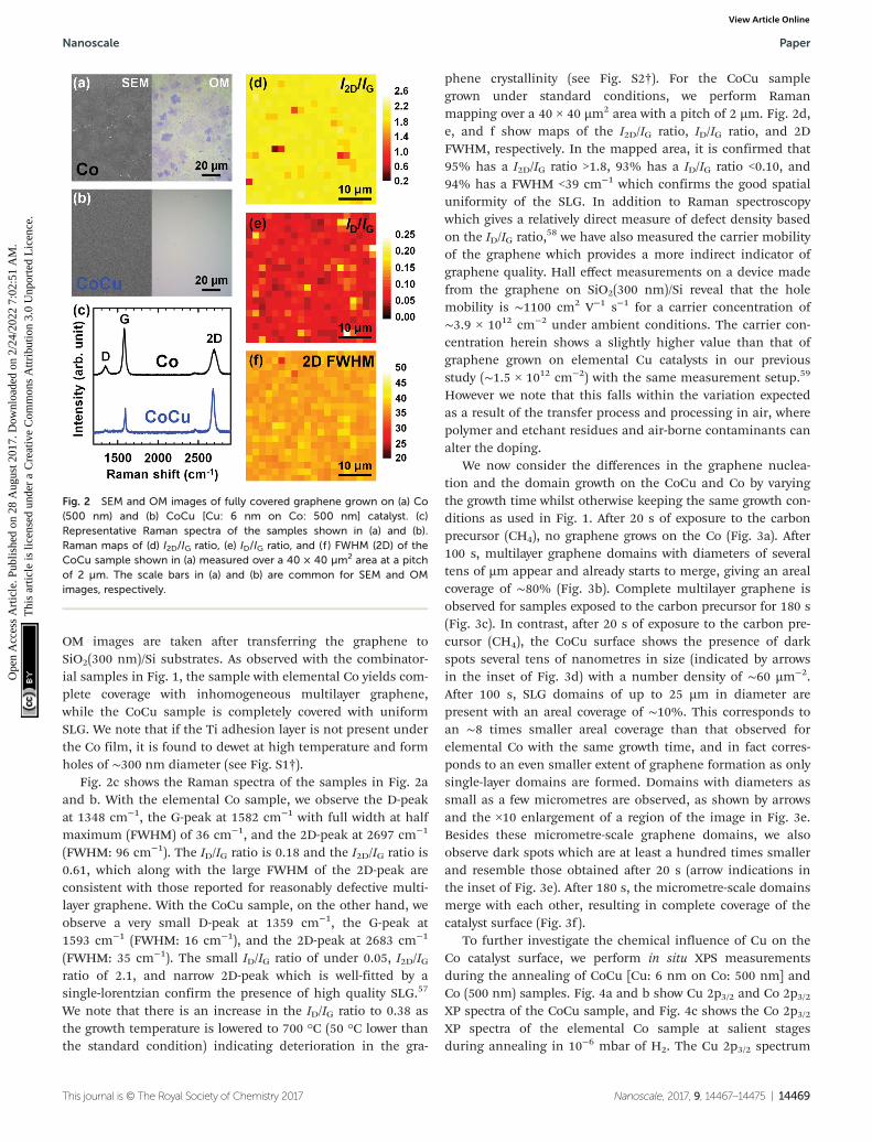
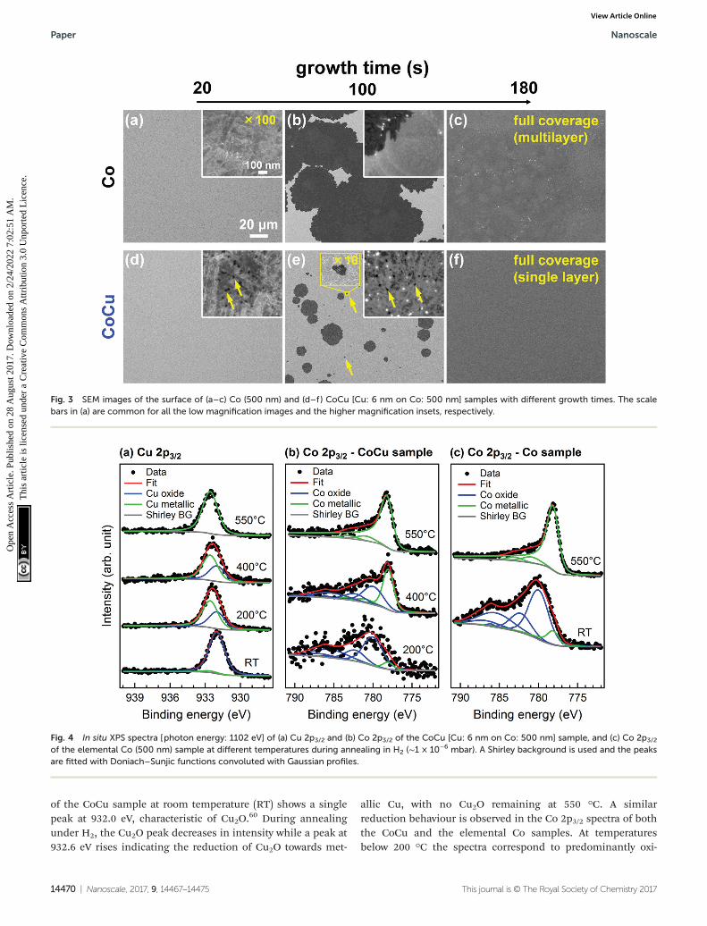
We now consider the differences in the graphene nuclea-tion and the domain growth on the CoCu and Co by varyingthe growth time whilst otherwise keeping the same growth con-ditions as used in Fig. 1. After 20 s of exposure to the carbonprecursor (CH4), no graphene grows on the Co (Fig. 3a). After100 s, multilayer graphene domains with diameters of severaltens of µm appear and already starts to merge, giving an arealcoverage of ∼80% (Fig. 3b). Complete multilayer graphene isobserved for samples exposed to the carbon precursor for 180 s(Fig. 3c). In contrast, after 20 s of exposure to the carbon pre-cursor (CH4), the CoCu surface shows the presence of darkspots several tens of nanometres in size (indicated by arrowsin the inset of Fig. 3d) with a number density of ∼60 µm−2.After 100 s, SLG domains of up to 25 µm in diameter arepresent with an areal coverage of ∼10%. This corresponds toan ∼8 times smaller areal coverage than that observed forelemental Co with the same growth time, and in fact corres-ponds to an even smaller extent of graphene formation as onlysingle-layer domains are formed. Domains with diameters assmall as a few micrometres are observed, as shown by arrowsand the ×10 enlargement of a region of the image in Fig. 3e.Besides these micrometre-scale graphene domains, we alsoobserve dark spots which are at least a hundred times smallerand resemble those obtained after 20 s (arrow indications inthe inset of Fig. 3e). After 180 s, the micrometre-scale domainsmerge with each other, resulting in complete coverage of thecatalyst surface (Fig. 3f).
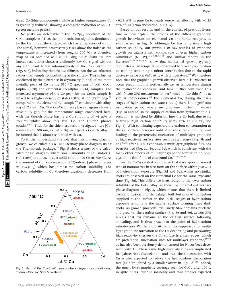
To further investigate the chemical influence of Cu on theCo catalyst surface, we perform in situ XPS measurementsduring the annealing of CoCu [Cu: 6 nm on Co: 500 nm] andCo (500 nm) samples. Fig. 4a and b show Cu 2p3/2 and Co 2p3/2XP spectra of the CoCu sample, and Fig. 4c shows the Co 2p3/2XP spectra of the elemental Co sample at salient stagesduring annealing in 10−6 mbar of H2. The Cu 2p3/2 spectrum
Fig. 2 SEM and OM images of fully covered graphene grown on (a) Co(500 nm) and (b) CoCu [Cu: 6 nm on Co: 500 nm] catalyst. (c)Representative Raman spectra of the samples shown in (a) and (b).Raman maps of (d) I2D/IG ratio, (e) ID/IG ratio, and (f ) FWHM (2D) of theCoCu sample shown in (a) measured over a 40 × 40 µm2 area at a pitchof 2 µm. The scale bars in (a) and (b) are common for SEM and OMimages, respectively.
Nanoscale Paper
This journal is © The Royal Society of Chemistry 2017 Nanoscale, 2017, 9, 14467–14475 | 14469
Ope
n A
cces
s A
rtic
le. P
ublis
hed
on 2
8 A
ugus
t 201
7. D
ownl
oade
d on
2/2
4/20
22 7
:02:
51 A
M.
Thi
s ar
ticle
is li
cens
ed u
nder
a C
reat
ive
Com
mon
s A
ttrib
utio
n 3.
0 U
npor
ted
Lic
ence
.View Article Online
of the CoCu sample at room temperature (RT) shows a singlepeak at 932.0 eV, characteristic of Cu2O.
60 During annealingunder H2, the Cu2O peak decreases in intensity while a peak at932.6 eV rises indicating the reduction of Cu2O towards met-
allic Cu, with no Cu2O remaining at 550 °C. A similarreduction behaviour is observed in the Co 2p3/2 spectra of boththe CoCu and the elemental Co samples. At temperaturesbelow 200 °C the spectra correspond to predominantly oxi-
Fig. 3 SEM images of the surface of (a–c) Co (500 nm) and (d–f ) CoCu [Cu: 6 nm on Co: 500 nm] samples with different growth times. The scalebars in (a) are common for all the low magnification images and the higher magnification insets, respectively.
Fig. 4 In situ XPS spectra [photon energy: 1102 eV] of (a) Cu 2p3/2 and (b) Co 2p3/2 of the CoCu [Cu: 6 nm on Co: 500 nm] sample, and (c) Co 2p3/2
of the elemental Co (500 nm) sample at different temperatures during annealing in H2 (∼1 × 10⁻⁶ mbar). A Shirley background is used and the peaksare fitted with Doniach–Sunjic functions convoluted with Gaussian profiles.
Paper Nanoscale
14470 | Nanoscale, 2017, 9, 14467–14475 This journal is © The Royal Society of Chemistry 2017
Ope
n A
cces
s A
rtic
le. P
ublis
hed
on 2
8 A
ugus
t 201
7. D
ownl
oade
d on
2/2
4/20
22 7
:02:
51 A
M.
Thi
s ar
ticle
is li
cens
ed u
nder
a C
reat
ive
Com
mon
s A
ttrib
utio
n 3.
0 U
npor
ted
Lic
ence
.View Article Online
dised Co (blue components), while at higher temperatures Cois gradually reduced, showing a complete reduction at 550 °C(green metallic peaks).
No peaks are detectable in the Co 2p3/2 spectrum of theCoCu sample at RT, as the photoemission signal is dominatedby the Cu film at the surface, which has a thickness of 6 nm.The signal, however, progressively rises above the noise as thetemperature is increased (from roughly 200 °C). A chemicalmap of Cu obtained at 550 °C using SPEM (with 100 nmlateral resolution) shows a uniformly low Cu signal withoutany significant lateral inhomogeneity in the Cu distribution(Fig. S3†), indicating that the Cu diffuses into the Co substraterather than simply redistributing at the surface. This is furtherconfirmed by the difference in asymmetry (alpha) of the mainmetallic peak of Co in the 550 °C spectrum of both CoCu(alpha ∼0.20) and elemental Co (alpha ∼0.14) samples. Theincreased asymmetry of the Co peak for the CoCu sample islinked to a higher density of states (DOS) at the Fermi edge61
compared to the elemental Co sample,62 consistent with alloy-ing of Co with Cu. The Co–Cu binary phase diagram shows amiscibility gap for the temperature range considered here,with the Co-rich phase having a Cu solubility of ∼1 at% at750 °C whilst above this level Co- and Cu-rich phasescoexist.63,64 Thus for the thickness ratio investigated here [Cu:6 nm on Co: 500 nm, i.e. ∼1 at%], we expect a Co-rich alloy tobe formed that is almost saturated with Cu.
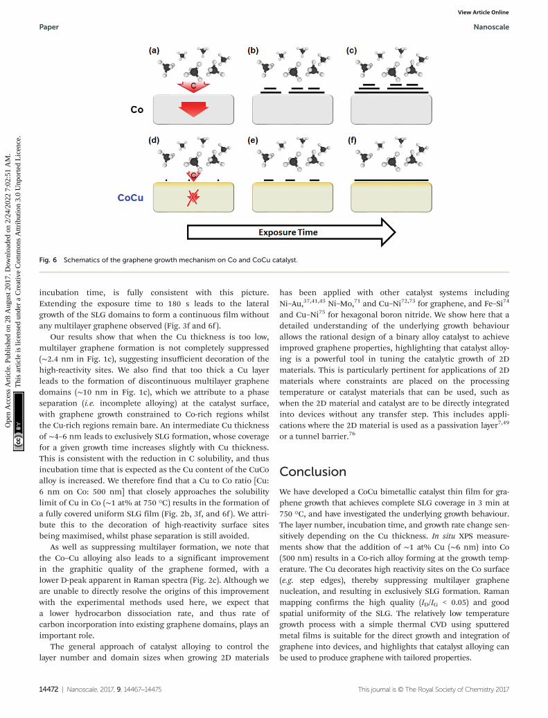
To further understand the role that this alloying plays ingrowth, we calculate a Co–Cu–C ternary phase diagram usingthe Thermo-calc package.65 Fig. 5 shows a part of the calcu-lated phase diagram where small amounts of Cu and/or C(≤0.4 at%) are present as a solid solution in Co at 750 °C. Asthe amount of Cu is increased, a FCC(ordered) phase emergesin FCC(L12) which has almost no carbon solubility. Thecarbon solubility in Co therefore drastically decreases from
∼0.23 at% in pure Co to nearly zero when alloying with ∼0.23at% of Cu (arrow indication in Fig. 5).
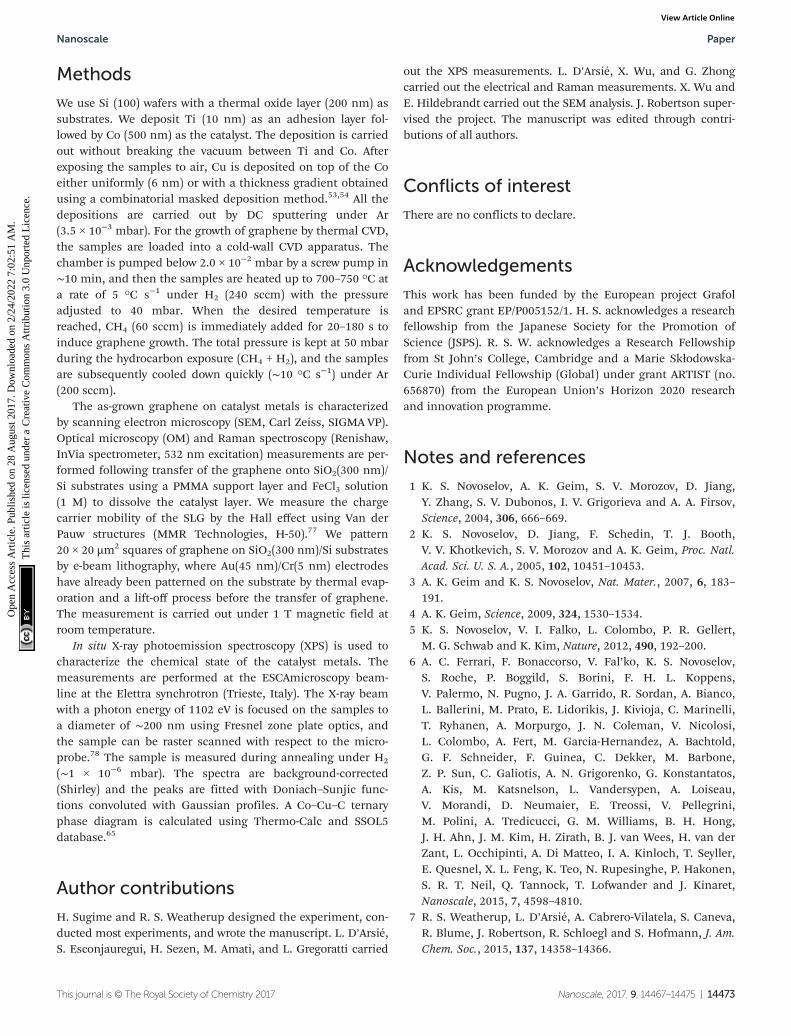
Based on our results, and in the context of previous litera-ture we now explain the origins of the different graphenegrowth behaviours on elemental Co and CoCu catalysts, assummarized in Fig. 6. Although Co has a relatively highcarbon solubility, our previous in situ studies of graphenegrowth on catalysts with comparable or even higher carbonsolubilities (Ni, Pt),37,39,41,43,44 and similar reports in theliterature35,36,38,42,66,67 show that isothermal growth typicallydominates at the temperature considered here, with precipitationon cooling remaining a minor contribution due to the rapiddecrease in carbon diffusivity with temperature.46 We thereforenote that the graphene growth observed herein is expected tooccur predominantly isothermally i.e. at temperature duringthe hydrocarbon exposure, and have further confirmed thiswith in situ XPS measurements performed on Co thin films atsimilar temperatures.68 For elemental Co, during the earlystages of hydrocarbon exposure (∼20 s) there is a significantincubation period where no graphene nucleation occurs(Fig. 3a and 6a) as the supply of carbon from hydrocarbon dis-sociation is matched by diffusion into the Co bulk due to itsrelatively high carbon solubility (0.23 at% at 750 °C, seeFig. 5). With continuing exposure the carbon concentration atthe Co surface increases until it exceeds the solubility limitleading to the preferential nucleation of multilayer grapheneat high reactivity surface sites such as step edges (Fig. 3b and6b).37,45 After 180 s, a continuous multilayer graphene film hasbeen formed (Fig. 2a, 3c, and 6c), which is consistent with themany other reports of multilayer graphene formation on poly-crystalline thin films of elemental Co.31–33,46,48
For the CoCu catalyst we observe that dark spots of severaltens of nanometres in size form on the surface within just 20 sof hydrocarbon exposure (Fig. 3d and 6d), whilst no similarspots are observed on the elemental Co for the same exposuretime (Fig. 3a). This difference is attributed to the lower carbonsolubility of the CoCu alloy, as shown by the Co–Cu–C ternaryphase diagram in Fig. 5, which means that there is limitedcarbon diffusion into the catalyst bulk but instead the carbonsupplied to the surface in the initial stages of hydrocarbonexposure remains at the catalyst surface forming these darkspots. As growth proceeds, exclusively SLG domains nucleateand grow on the catalyst surface (Fig. 3e and 6e). In situ XPSreveals that Cu remains at the catalyst surface followingannealing, and is thus present at the point of hydrocarbonintroduction. We therefore attribute this suppression of multi-layer graphene formation to the Cu decorating and passivatinghigh reactivity sites on the Co surface (e.g. step edges) whichare preferential nucleation sites for multilayer graphene,69,70
as has also been previously demonstrated for Ni surfaces deco-rated with Au. These same high reactivity sites are implicatedin hydrocarbon dissociation, and thus their decoration withCu is also expected to reduce the hydrocarbon dissociationrate (as highlighted by a smaller arrow in Fig. 6d).23 Indeed,the much lower graphene coverage seen for CoCu after 100 s,in spite of its lower C solubility and thus smaller expected
Fig. 5 Part of the Co–Cu–C ternary phase diagram calculated usingThermo-Calc and SSOL5 database.
Nanoscale Paper
This journal is © The Royal Society of Chemistry 2017 Nanoscale, 2017, 9, 14467–14475 | 14471
Ope
n A
cces
s A
rtic
le. P
ublis
hed
on 2
8 A
ugus
t 201
7. D
ownl
oade
d on
2/2
4/20
22 7
:02:
51 A
M.
Thi
s ar
ticle
is li
cens
ed u
nder
a C
reat
ive
Com
mon
s A
ttrib
utio
n 3.
0 U
npor
ted
Lic
ence
.View Article Online
incubation time, is fully consistent with this picture.Extending the exposure time to 180 s leads to the lateralgrowth of the SLG domains to form a continuous film withoutany multilayer graphene observed (Fig. 3f and 6f).
Our results show that when the Cu thickness is too low,multilayer graphene formation is not completely suppressed(∼2.4 nm in Fig. 1c), suggesting insufficient decoration of thehigh-reactivity sites. We also find that too thick a Cu layerleads to the formation of discontinuous multilayer graphenedomains (∼10 nm in Fig. 1c), which we attribute to a phaseseparation (i.e. incomplete alloying) at the catalyst surface,with graphene growth constrained to Co-rich regions whilstthe Cu-rich regions remain bare. An intermediate Cu thicknessof ∼4–6 nm leads to exclusively SLG formation, whose coveragefor a given growth time increases slightly with Cu thickness.This is consistent with the reduction in C solubility, and thusincubation time that is expected as the Cu content of the CuCoalloy is increased. We therefore find that a Cu to Co ratio [Cu:6 nm on Co: 500 nm] that closely approaches the solubilitylimit of Cu in Co (∼1 at% at 750 °C) results in the formation ofa fully covered uniform SLG film (Fig. 2b, 3f, and 6f). We attri-bute this to the decoration of high-reactivity surface sitesbeing maximised, whilst phase separation is still avoided.
As well as suppressing multilayer formation, we note thatthe Co–Cu alloying also leads to a significant improvementin the graphitic quality of the graphene formed, with alower D-peak apparent in Raman spectra (Fig. 2c). Although weare unable to directly resolve the origins of this improvementwith the experimental methods used here, we expect thata lower hydrocarbon dissociation rate, and thus rate ofcarbon incorporation into existing graphene domains, plays animportant role.
The general approach of catalyst alloying to control thelayer number and domain sizes when growing 2D materials
has been applied with other catalyst systems includingNi–Au,37,41,45 Ni–Mo,71 and Cu–Ni72,73 for graphene, and Fe–Si74
and Cu–Ni75 for hexagonal boron nitride. We show here that adetailed understanding of the underlying growth behaviourallows the rational design of a binary alloy catalyst to achieveimproved graphene properties, highlighting that catalyst alloy-ing is a powerful tool in tuning the catalytic growth of 2Dmaterials. This is particularly pertinent for applications of 2Dmaterials where constraints are placed on the processingtemperature or catalyst materials that can be used, such aswhen the 2D material and catalyst are to be directly integratedinto devices without any transfer step. This includes appli-cations where the 2D material is used as a passivation layer7,49
or a tunnel barrier.76
Conclusion
We have developed a CoCu bimetallic catalyst thin film for gra-phene growth that achieves complete SLG coverage in 3 min at750 °C, and have investigated the underlying growth behaviour.The layer number, incubation time, and growth rate change sen-sitively depending on the Cu thickness. In situ XPS measure-ments show that the addition of ∼1 at% Cu (∼6 nm) into Co(500 nm) results in a Co-rich alloy forming at the growth temp-erature. The Cu decorates high reactivity sites on the Co surface(e.g. step edges), thereby suppressing multilayer graphenenucleation, and resulting in exclusively SLG formation. Ramanmapping confirms the high quality (ID/IG < 0.05) and goodspatial uniformity of the SLG. The relatively low temperaturegrowth process with a simple thermal CVD using sputteredmetal films is suitable for the direct growth and integration ofgraphene into devices, and highlights that catalyst alloying canbe used to produce graphene with tailored properties.
Fig. 6 Schematics of the graphene growth mechanism on Co and CoCu catalyst.
Paper Nanoscale
14472 | Nanoscale, 2017, 9, 14467–14475 This journal is © The Royal Society of Chemistry 2017
Ope
n A
cces
s A
rtic
le. P
ublis
hed
on 2
8 A
ugus
t 201
7. D
ownl
oade
d on
2/2
4/20
22 7
:02:
51 A
M.
Thi
s ar
ticle
is li
cens
ed u
nder
a C
reat
ive
Com
mon
s A
ttrib
utio
n 3.
0 U
npor
ted
Lic
ence
.View Article Online
Methods
We use Si (100) wafers with a thermal oxide layer (200 nm) assubstrates. We deposit Ti (10 nm) as an adhesion layer fol-lowed by Co (500 nm) as the catalyst. The deposition is carriedout without breaking the vacuum between Ti and Co. Afterexposing the samples to air, Cu is deposited on top of the Coeither uniformly (6 nm) or with a thickness gradient obtainedusing a combinatorial masked deposition method.53,54 All thedepositions are carried out by DC sputtering under Ar(3.5 × 10⁻³ mbar). For the growth of graphene by thermal CVD,the samples are loaded into a cold-wall CVD apparatus. Thechamber is pumped below 2.0 × 10⁻² mbar by a screw pump in∼10 min, and then the samples are heated up to 700–750 °C ata rate of 5 °C s−1 under H2 (240 sccm) with the pressureadjusted to 40 mbar. When the desired temperature isreached, CH4 (60 sccm) is immediately added for 20–180 s toinduce graphene growth. The total pressure is kept at 50 mbarduring the hydrocarbon exposure (CH4 + H2), and the samplesare subsequently cooled down quickly (∼10 °C s−1) under Ar(200 sccm).
The as-grown graphene on catalyst metals is characterizedby scanning electron microscopy (SEM, Carl Zeiss, SIGMA VP).Optical microscopy (OM) and Raman spectroscopy (Renishaw,InVia spectrometer, 532 nm excitation) measurements are per-formed following transfer of the graphene onto SiO2(300 nm)/Si substrates using a PMMA support layer and FeCl3 solution(1 M) to dissolve the catalyst layer. We measure the chargecarrier mobility of the SLG by the Hall effect using Van derPauw structures (MMR Technologies, H-50).77 We pattern20 × 20 µm2 squares of graphene on SiO2(300 nm)/Si substratesby e-beam lithography, where Au(45 nm)/Cr(5 nm) electrodeshave already been patterned on the substrate by thermal evap-oration and a lift-off process before the transfer of graphene.The measurement is carried out under 1 T magnetic field atroom temperature.
In situ X-ray photoemission spectroscopy (XPS) is used tocharacterize the chemical state of the catalyst metals. Themeasurements are performed at the ESCAmicroscopy beam-line at the Elettra synchrotron (Trieste, Italy). The X-ray beamwith a photon energy of 1102 eV is focused on the samples toa diameter of ∼200 nm using Fresnel zone plate optics, andthe sample can be raster scanned with respect to the micro-probe.78 The sample is measured during annealing under H2
(∼1 × 10⁻⁶ mbar). The spectra are background-corrected(Shirley) and the peaks are fitted with Doniach–Sunjic func-tions convoluted with Gaussian profiles. A Co–Cu–C ternaryphase diagram is calculated using Thermo-Calc and SSOL5database.65
Author contributions
H. Sugime and R. S. Weatherup designed the experiment, con-ducted most experiments, and wrote the manuscript. L. D’Arsié,S. Esconjauregui, H. Sezen, M. Amati, and L. Gregoratti carried
out the XPS measurements. L. D’Arsié, X. Wu, and G. Zhongcarried out the electrical and Raman measurements. X. Wu andE. Hildebrandt carried out the SEM analysis. J. Robertson super-vised the project. The manuscript was edited through contri-butions of all authors.
Conflicts of interest
There are no conflicts to declare.
Acknowledgements
This work has been funded by the European project Grafoland EPSRC grant EP/P005152/1. H. S. acknowledges a researchfellowship from the Japanese Society for the Promotion ofScience (JSPS). R. S. W. acknowledges a Research Fellowshipfrom St John’s College, Cambridge and a Marie Skłodowska-Curie Individual Fellowship (Global) under grant ARTIST (no.656870) from the European Union’s Horizon 2020 researchand innovation programme.
Notes and references
1 K. S. Novoselov, A. K. Geim, S. V. Morozov, D. Jiang,Y. Zhang, S. V. Dubonos, I. V. Grigorieva and A. A. Firsov,Science, 2004, 306, 666–669.
2 K. S. Novoselov, D. Jiang, F. Schedin, T. J. Booth,V. V. Khotkevich, S. V. Morozov and A. K. Geim, Proc. Natl.Acad. Sci. U. S. A., 2005, 102, 10451–10453.
3 A. K. Geim and K. S. Novoselov, Nat. Mater., 2007, 6, 183–191.
4 A. K. Geim, Science, 2009, 324, 1530–1534.5 K. S. Novoselov, V. I. Falko, L. Colombo, P. R. Gellert,
M. G. Schwab and K. Kim, Nature, 2012, 490, 192–200.6 A. C. Ferrari, F. Bonaccorso, V. Fal’ko, K. S. Novoselov,
S. Roche, P. Boggild, S. Borini, F. H. L. Koppens,V. Palermo, N. Pugno, J. A. Garrido, R. Sordan, A. Bianco,L. Ballerini, M. Prato, E. Lidorikis, J. Kivioja, C. Marinelli,T. Ryhanen, A. Morpurgo, J. N. Coleman, V. Nicolosi,L. Colombo, A. Fert, M. Garcia-Hernandez, A. Bachtold,G. F. Schneider, F. Guinea, C. Dekker, M. Barbone,Z. P. Sun, C. Galiotis, A. N. Grigorenko, G. Konstantatos,A. Kis, M. Katsnelson, L. Vandersypen, A. Loiseau,V. Morandi, D. Neumaier, E. Treossi, V. Pellegrini,M. Polini, A. Tredicucci, G. M. Williams, B. H. Hong,J. H. Ahn, J. M. Kim, H. Zirath, B. J. van Wees, H. van derZant, L. Occhipinti, A. Di Matteo, I. A. Kinloch, T. Seyller,E. Quesnel, X. L. Feng, K. Teo, N. Rupesinghe, P. Hakonen,S. R. T. Neil, Q. Tannock, T. Lofwander and J. Kinaret,Nanoscale, 2015, 7, 4598–4810.
7 R. S. Weatherup, L. D’Arsié, A. Cabrero-Vilatela, S. Caneva,R. Blume, J. Robertson, R. Schloegl and S. Hofmann, J. Am.Chem. Soc., 2015, 137, 14358–14366.
Nanoscale Paper
This journal is © The Royal Society of Chemistry 2017 Nanoscale, 2017, 9, 14467–14475 | 14473
Ope
n A
cces
s A
rtic
le. P
ublis
hed
on 2
8 A
ugus
t 201
7. D
ownl
oade
d on
2/2
4/20
22 7
:02:
51 A
M.
Thi
s ar
ticle
is li
cens
ed u
nder
a C
reat
ive
Com
mon
s A
ttrib
utio
n 3.
0 U
npor
ted
Lic
ence
.View Article Online
8 S. Hofmann, P. Braeuninger-Weimer and R. S. Weatherup,J. Phys. Chem. Lett., 2015, 6, 2714–2721.
9 G. Zhong, X. Wu, L. D’Arsie, K. B. K. Teo, N. L. Rupesinghe,A. Jouvray and J. Robertson, Appl. Phys. Lett., 2016, 109,193103.
10 X. S. Li, W. W. Cai, J. H. An, S. Kim, J. Nah, D. X. Yang,R. Piner, A. Velamakanni, I. Jung, E. Tutuc, S. K. Banerjee,L. Colombo and R. S. Ruoff, Science, 2009, 324, 1312–1314.
11 X. Li, W. Cai, L. Colombo and R. S. Ruoff, Nano Lett., 2009,9, 4268–4272.
12 X. Li, C. W. Magnuson, A. Venugopal, R. M. Tromp,J. B. Hannon, E. M. Vogel, L. Colombo and R. S. Ruoff,J. Am. Chem. Soc., 2011, 133, 2816–2819.
13 H. Zhou, W. J. Yu, L. Liu, R. Cheng, Y. Chen, X. Huang,Y. Liu, Y. Wang, Y. Huang and X. Duan, Nat. Commun.,2013, 4, 2096.
14 X. Wu, G. F. Zhong, L. D’Arsié, H. Sugime,S. Esconjauregui, A. W. Robertson and J. Robertson, Sci.Rep., 2016, 6, 21152.
15 R. Muñoz and C. Gomez-Aleixandre, Chem. VaporDeposition, 2013, 19, 297–322.
16 M. Kratzer, B. C. Bayer, P. R. Kidambi, A. Matković,R. Gajić, A. Cabrero-Vilatela, R. S. Weatherup, S. Hofmannand C. Teichert, Appl. Phys. Lett., 2015, 106, 103101.
17 P. R. Kidambi, C. Ducati, B. Dlubak, D. Gardiner,R. S. Weatherup, M.-B. Martin, P. Seneor, H. Coles andS. Hofmann, J. Phys. Chem. C, 2012, 116, 22492–22501.
18 B. Dlubak, M.-B. Martin, R. S. Weatherup, H. Yang,C. Deranlot, R. Blume, R. Schloegl, A. Fert, A. Anane,S. Hofmann, P. Seneor and J. Robertson, ACS Nano, 2012,6, 10930–10934.
19 M.-B. Martin, B. Dlubak, R. S. Weatherup, H. Yang,C. Deranlot, K. Bouzehouane, F. Petroff, A. Anane,S. Hofmann, J. Robertson, A. Fert and P. Seneor, ACS Nano,2014, 8, 7890–7895.
20 M. Nihei, A. Kawabata and Y. Awano, Jpn. J. Appl. Phys.,2003, 42, L721–L723.
21 M. Cantoro, S. Hofmann, S. Pisana, V. Scardaci, A. Parvez,C. Ducati, A. C. Ferrari, A. M. Blackburn, K. Y. Wang andJ. Robertson, Nano Lett., 2006, 6, 1107–1112.
22 D. Yokoyama, T. Iwasaki, K. Ishimaru, S. Sato,T. Hyakushima, M. Nihei, Y. Awano and H. Kawarada,Jpn. J. Appl. Phys., 2008, 47, 1985–1990.
23 J. Robertson, J. Mater. Chem., 2012, 22, 19858–19862.24 H. Sugime, S. Esconjauregui, J. W. Yang, L. D’Arsié,
R. A. Oliver, S. Bhardwaj, C. Cepek and J. Robertson, Appl.Phys. Lett., 2013, 103, 073116.
25 H. Sugime, S. Esconjauregui, L. D’Arsié, J. W. Yang,T. Makaryan and J. Robertson, ACS Appl. Mater. Interfaces,2014, 6, 15440–15447.
26 N. Na, D. Y. Kim, Y. G. So, Y. Ikuhara and S. Noda, Carbon,2015, 81, 773–781.
27 H. Sugime, S. Esconjauregui, L. D’Arsié, J. Yang,A. W. Robertson, R. A. Oliver, S. Bhardwaj, C. Cepek andJ. Robertson, ACS Appl. Mater. Interfaces, 2015, 7, 16819–16827.
28 Q. Yu, J. Lian, S. Siriponglert, H. Li, Y. P. Chen andS.-S. Pei, Appl. Phys. Lett., 2008, 93, 113103.
29 A. Reina, X. Jia, J. Ho, D. Nezich, H. Son, V. Bulovic,M. S. Dresselhaus and J. Kong, Nano Lett., 2009, 9, 30–35.
30 K. S. Kim, Y. Zhao, H. Jang, S. Y. Lee, J. M. Kim, J. H. Ahn,P. Kim, J. Y. Choi and B. H. Hong, Nature, 2009, 457, 706–710.
31 M. E. Ramón, A. Gupta, C. Corbet, D. A. Ferrer,H. C. P. Movva, G. Carpenter, L. Colombo, G. Bourianoff,M. Doczy, D. Akinwande, E. Tutuc and S. K. Banerjee, ACSNano, 2011, 5, 7198–7204.
32 S. M. Wang, Y. H. Pei, X. Wang, H. Wang, Q. N. Meng,H. W. Tian, X. L. Zheng, W. T. Zheng and Y. C. Liu, J. Phys.D: Appl. Phys., 2010, 43, 455402.
33 N. Zhan, G. Wang and J. Liu, Appl. Phys. A, 2011, 105, 341–345.
34 A. Reina, S. Thiele, X. T. Jia, S. Bhaviripudi,M. S. Dresselhaus, J. A. Schaefer and J. Kong, Nano Res.,2009, 2, 509–516.
35 A. Gruneis, K. Kummer and D. V. Vyalikh, New J. Phys.,2009, 11, 073050.
36 K. L. Saenger, J. C. Tsang, A. A. Bol, J. O. Chu, A. Grill andC. Lavoie, Appl. Phys. Lett., 2010, 96, 153105.
37 R. S. Weatherup, B. C. Bayer, R. Blume, C. Ducati,C. Baehtz, R. Schlogl and S. Hofmann, Nano Lett., 2011, 11,4154–4160.
38 R. Addou, A. Dahal, P. Sutter and M. Batzill, Appl. Phys.Lett., 2012, 100, 021601.
39 R. S. Weatherup, B. C. Bayer, R. Blume, C. Baehtz,P. R. Kidambi, M. Fouquet, C. T. Wirth, R. Schlogl andS. Hofmann, ChemPhysChem, 2012, 13, 2544–2549.
40 L. L. Patera, C. Africh, R. S. Weatherup, R. Blume,S. Bhardwaj, C. Castellarin-Cudia, A. Knop-Gericke,R. Schloegl, G. Comelli, S. Hofmann and C. Cepek, ACSNano, 2013, 7, 7901–7912.
41 R. S. Weatherup, C. Baehtz, B. Dlubak, B. C. Bayer,P. R. Kidambi, R. Blume, R. Schloegl and S. Hofmann,Nano Lett., 2013, 13, 4624–4631.
42 A. A. Puretzky, D. B. Geohegan, S. Pannala, C. M. Rouleau,M. Regmi, N. Thonnard and G. Eres, Nanoscale, 2013, 5,6507–6517.
43 R. S. Weatherup, H. Amara, R. Blume, B. Dlubak,B. C. Bayer, M. Diarra, M. Bahri, A. Cabrero-Vilatela,S. Caneva, P. R. Kidambi, M. B. Martin, C. Deranlot,P. Seneor, R. Schloegl, F. Ducastelle, C. Bichara andS. Hofmann, J. Am. Chem. Soc., 2014, 136, 13698–13708.
44 R. S. Weatherup, A. J. Shahani, Z.-J. Wang, K. Mingard,A. J. Pollard, M.-G. Willinger, R. Schloegl, P. W. Voorheesand S. Hofmann, Nano Lett., 2016, 16, 6196–6206.
45 R. S. Weatherup, B. Dlubak and S. Hofmann, ACS Nano,2012, 6, 9996–10003.
46 A. Cabrero-Vilatela, R. S. Weatherup, P. Braeuninger-Weimer, S. Caneva and S. Hofmann, Nanoscale, 2016, 8,2149–2158.
47 C. Oshima and A. Nagashima, J. Phys.: Condens. Matter,1997, 9, 1–20.
Paper Nanoscale
14474 | Nanoscale, 2017, 9, 14467–14475 This journal is © The Royal Society of Chemistry 2017
Ope
n A
cces
s A
rtic
le. P
ublis
hed
on 2
8 A
ugus
t 201
7. D
ownl
oade
d on
2/2
4/20
22 7
:02:
51 A
M.
Thi
s ar
ticle
is li
cens
ed u
nder
a C
reat
ive
Com
mon
s A
ttrib
utio
n 3.
0 U
npor
ted
Lic
ence
.View Article Online
48 H. Ago, Y. Ito, N. Mizuta, K. Yoshida, B. Hu, C. M. Orofeo,M. Tsuji, K. Ikeda and S. Mizuno, ACS Nano, 2010, 4, 7407–7414.
49 M.-B. Martin, B. Dlubak, R. S. Weatherup, M. Piquemal-Banci, H. Yang, R. Blume, R. Schloegl, S. Collin, F. Petroff,S. Hofmann, J. Robertson, A. Anane, A. Fert and P. Seneor,Appl. Phys. Lett., 2015, 107, 012408.
50 H. Yang, A. D. Vu, A. Hallal, N. Rougemaille, J. Coraux,G. Chen, A. K. Schmid and M. Chshiev, Nano Lett., 2016,16, 145–151.
51 J. Coraux, A. T. N’Diaye, N. Rougemaille, C. Vo-Van,A. Kimouche, H.-X. Yang, M. Chshiev, N. Bendiab, O. Fruchartand A. K. Schmid, J. Phys. Chem. Lett., 2012, 3, 2059–2063.
52 V. M. Karpan, P. A. Khomyakov, A. A. Starikov,G. Giovannetti, M. Zwierzycki, M. Talanana, G. Brocks,J. van den Brink and P. J. Kelly, Phys. Rev. B: Condens.Matter, 2008, 78, 195419.
53 S. Noda, H. Sugime, T. Osawa, Y. Tsuji, S. Chiashi,Y. Murakami and S. Maruyama, Carbon, 2006, 44, 1414–1419.
54 H. Sugime, S. Noda, S. Maruyama and Y. Yamaguchi,Carbon, 2009, 47, 234–241.
55 P. Blake, E. W. Hill, A. H. Castro Neto, K. S. Novoselov,D. Jiang, R. Yang, T. J. Booth and A. K. Geim, Appl. Phys.Lett., 2007, 91, 063124.
56 C. Casiraghi, A. Hartschuh, E. Lidorikis, H. Qian,H. Harutyunyan, T. Gokus, K. S. Novoselov andA. C. Ferrari, Nano Lett., 2007, 7, 2711–2717.
57 A. C. Ferrari, J. C. Meyer, V. Scardaci, C. Casiraghi,M. Lazzeri, F. Mauri, S. Piscanec, D. Jiang, K. S. Novoselov,S. Roth and A. K. Geim, Phys. Rev. Lett., 2006, 97, 187401.
58 F. Tuinstra and J. L. Koenig, J. Chem. Phys., 1970, 53, 1126–1130.
59 L. D’Arsié, S. Esconjauregui, R. S. Weatherup, X. Wu,W. E. Arter, H. Sugime, C. Cepek and J. Robertson, RSCAdv., 2016, 6, 113185–113192.
60 M. C. Biesinger, L. W. M. Lau, A. R. Gerson andR. S. C. Smart, Appl. Surf. Sci., 2010, 257, 887–898.
61 J.-M. Dubois, E. Belin-Ferre and K. Urban, Complex MetallicAlloys: Fundamentals and Applications, John Wiley & Sons,2010, p. 173.
62 G. Collinge, Y. Z. Xiang, R. Barbosa, J. S. McEwen andN. Kruse, Surf. Sci., 2016, 648, 74–83.
63 F. J. Bruni and J. W. Christian, Mater. Sci. Eng., 1972, 9,241–242.
64 M. Palumbo, S. Curiotto and L. Battezzati, CALPHAD:Comput. Coupling Phase Diagrams Thermochem., 2006, 30,171–178.
65 J. O. Andersson, T. Helander, L. H. Hoglund, P. F. Shi andB. Sundman, CALPHAD: Comput. Coupling Phase DiagramsThermochem., 2002, 26, 273–312.
66 J. C. Shelton, H. R. Patil and J. M. Blakely, Surf. Sci., 1974,43, 493–520.
67 P. Zhao, B. Hou, X. Chen, S. Kim, S. Chiashi, E. Einarssonand S. Maruyama, Nanoscale, 2013, 5, 6530–6537.
68 R. S. Weatherup, et al., in preparation.69 F. Besenbacher, I. Chorkendorff, B. S. Clausen,
B. Hammer, A. M. Molenbroek, J. K. Nørskov andI. Stensgaard, Science, 1998, 279, 1913–1915.
70 S. Saadi, F. Abild-Pedersen, S. Helveg, J. Sehested,B. Hinnemann, C. C. Appel and J. K. Nørskov, J. Phys.Chem. C, 2010, 114, 11221–11227.
71 B. Y. Dai, L. Fu, Z. Y. Zou, M. Wang, H. T. Xu, S. Wang andZ. F. Liu, Nat. Commun., 2011, 2, 522.
72 N. Liu, L. Fu, B. Dai, K. Yan, X. Liu, R. Zhao, Y. Zhang andZ. Liu, Nano Lett., 2011, 11, 297–303.
73 Y. Wu, H. Chou, H. Ji, Q. Wu, S. Chen, W. Jiang, Y. Hao,J. Kang, Y. Ren, R. D. Piner and R. S. Ruoff, ACS Nano,2012, 6, 7731–7738.
74 S. Caneva, R. S. Weatherup, B. C. Bayer, B. Brennan,S. J. Spencer, K. Mingard, A. Cabrero-Vilatela, C. Baehtz,A. J. Pollard and S. Hofmann, Nano Lett., 2015, 15, 1867–1875.
75 G. Lu, T. Wu, Q. Yuan, H. Wang, H. Wang, F. Ding, X. Xieand M. Jiang, Nat. Commun., 2015, 6, 6160.
76 M. Piquemal-Banci, R. Galceran, S. Caneva, M.-B. Martin,R. S. Weatherup, P. R. Kidambi, K. Bouzehouane, S. Xavier,A. Anane, F. Petroff, A. Fert, J. Robertson, S. Hofmann,B. Dlubak and P. Seneor, Appl. Phys. Lett., 2016, 108,102404.
77 A. Venugopal, J. Chan, X. Li, C. W. Magnuson, W. P. Kirk,L. Colombo, R. S. Ruoff and E. M. Vogel, J. Appl. Phys.,2011, 109, 104511.
78 M. K. Abyaneh, L. Gregoratti, M. Amati, M. Dalmiglio andM. Kiskinova, e-J. Surf. Sci. Nanotechnol., 2011, 9, 158–162.
Nanoscale Paper
This journal is © The Royal Society of Chemistry 2017 Nanoscale, 2017, 9, 14467–14475 | 14475
Ope
n A
cces
s A
rtic
le. P
ublis
hed
on 2
8 A
ugus
t 201
7. D
ownl
oade
d on
2/2
4/20
22 7
:02:
51 A
M.
Thi
s ar
ticle
is li
cens
ed u
nder
a C
reat
ive
Com
mon
s A
ttrib
utio
n 3.
0 U
npor
ted
Lic
ence
.View Article Online


![[Darnet][[ditedi] over layer 7 firewalling](https://static.fdocumenti.com/doc/165x107/559956d31a28ab8f408b47e8/darnetditedi-over-layer-7-firewalling.jpg)